
Ultrafast growth of submillimeter-scale single-crystal MoSe2 by pre-alloying CVD†
Xing
Xin‡
ab,
Jiamei
Chen‡
a,
Yanmei
Zhang
a,
Mao-Lin
Chen
c,
Youzhe
Bao
a,
Weizhen
Liu
a,
Yichun
Liu
a,
Haiyang
Xu
 *a and
Wencai
Ren
*bd
*a and
Wencai
Ren
*bd
aCentre for Advanced Optoelectronic Functional Materials Research and Key Laboratory of UV-Emitting Materials and Technology, Northeast Normal University, Ministry of Education, Changchun 130024, China. E-mail: hyxu@nenu.edu.cn
bShenyang National Laboratory for Materials Science, Institute of Metal Research, Chinese Academy of Science, Shenyang 110016, P. R. China. E-mail: wcren@imr.ac.cn
cState Key Laboratory of Quantum Optics and Quantum Optics Devices, Institute of Optoelectronics, Shanxi University, Taiyuan 03006, China
dSchool of Material Science and Engineering, University of Science and Technology of China, Shenyang 110016, P. R. China
First published on 12th April 2022
Abstract
The synthesis of large-scale monolayer single-crystal MX2 (M = Mo, W; X = S, Se), a typical transition metal dichalcogenide (TMD), is the premise for their future applications. Compared with insulating substrates such as SiO2 and sapphire, Au is more favourable for the fast growth of TMDs by chemical vapor deposition (CVD). Recently, large-scale single-crystal WX2 was successfully grown and transferred on Au. In sharp contrast, the growth and transfer for monolayer MoX2 is still very challenging, because Au has a higher solubility of Mo and stronger interaction with MoX2 than WX2. Compared with the most studied MoS2, MoSe2 is superior in many aspects because of the narrower band gap and tunable excitonic charging effects. However, the synthesis of large-scale single-crystal MoSe2 on Au has not been reported so far. Here, a pre-alloying CVD method was developed to solve the problems for the growth and non-destructive transfer of MoX2. It has realized the ultrafast growth (30 s) of submillimeter-scale (560 μm) single-crystal MoSe2 for the first time. As-grown samples are strictly monolayers with good optical and electrical properties, which can be easily transferred without sacrificing Au foils by the electrochemical bubbling method. It was found that pre-alloying not only passivates the energetically active sites on Au but also weakens the interaction between Au and MoSe2, which is responsible for the ultrafast growth and easy transfer of MoSe2. This method is also universal for the fast growth and non-destructive transfer of other 2D TMDs.
New conceptsUltrafast growth of 2D materials is one of the hot research topics, which is not only beneficial for the synthesis of large-scale 2D materials but also can greatly reduce the production cost. Among 2D materials, monolayer transition metal dichalcogenides (TMDs) are highly desired for electronic and optoelectronic applications. Although numerous efforts have been devoted to such materials, the ultrafast growth and transfer of large-scale monolayer single-crystal TMDs is still challenging. Here, a new pre-alloying CVD method was developed to solve the problems for the growth and transfer of MoX2. It has realized the ultrafast growth and non-destructive transfer of submillimeter-scale monolayer single-crystal MoSe2 for the first time. We also discussed the growth mechanism and confirmed it is universal for other 2D TMDs. Pre-alloying CVD offers important insights for the synthesis of large-scale high-quality TMDs and other 2D materials, which paves the way for their electronic and optoelectronic applications. |
Introduction
Due to the direct band gap structure, monolayer two-dimensional (2D) MX2 (M = Mo, W; X = S, Se) transition metal dichalcogenides (TMDs) have attracted much attention for their unique properties and promising electronic and optoelectronic applications.1–5 However, defects, grain boundaries and the uniformity of layer-number intensively influence their various properties.6–9 On the other hand, ultrafast growth of 2D materials is one research focus. It is not only beneficial for the synthesis of large-scale 2D materials, but also can greatly reduce the production cost by shortening the growth time during the energy-consuming chemical vapor deposition (CVD) process.10–13 Therefore, the ultrafast growth of large-scale, high-quality and uniform monolayer MX2 single crystals is essential for their future applications. Recently, numerous efforts have been devoted to growing such materials on various substrates. Insulating substrates (SiO2/Si, sapphire, mica and so on) have poor catalytic activity, resulting in the low growth rate and limited grain size of monolayer MX2.14–17 Moreover, many defects (vacancies, adatoms etc.) and uncontrollable multilayers were inevitably formed during TMD growth on these substrates. By contrast, Au is a good candidate for the fast growth of large-scale high-quality uniform monolayer MX2 because of its catalytic effects.10,18–21The very low solubility of W in Au (∼0.08 at% at 1050 °C)22 makes WX2 on Au follow the self-limited catalytic surface growth mechanism. In our previous reports, we have demonstrated the synthesis of millimeter-sized single-crystal WS2 and WSe2 by using Au foils.10,19 WX2 can be easily transferred from Au foils because of the weak interaction between WX2 and Au. In sharp contrast, Au has a higher solubility of Mo (∼1.25 at% at 1050 °C)23 than W. Although MoS2 has been achieved on Au, the growth rate was very low (∼0.03 μm s−1).24–26 Furthermore, Au substrates had to be etched away when transferring MoS2 for subsequent applications because of the strong interaction between MoX2 and Au. Compared with the most studied MoS2, MoSe2 is superior in many aspects because of the narrower band gap (1.5 eV for MoSe2 and 1.9 eV for MoS2) and tunable excitonic charging effects.27–30 However, the synthesis of large-scale single-crystal monolayer MoSe2 on Au has not been realized so far.
Here, we develop a pre-alloying CVD method to solve the problems for the growth and transfer of MoX2 on Au and realize the ultrafast growth of submillimeter-scale single-crystal MoSe2 for the first time. 560 μm-large MoSe2 triangles were synthesized in 30 s with an ultrahigh growth rate of ∼18.7 μm s−1. As-grown samples are strictly monolayer with good optical and electrical properties, which were easily transferred without sacrificing Au foils by the electrochemical bubbling method. We also revealed that pre-alloying can not only passivate the energetically active sites on Au but also weaken the interaction between MoSe2 and Au, which is responsible for the ultrafast growth and easy transfer of MoSe2. Finally, we demonstrated that pre-alloying CVD is applicable for the fast growth and non-destructive transfer of other 2D TMDs. The growth rate of as-grown 450 μm-large single-crystal MoS2 was increased by over 100 times compared to those reported works.24–26
Experimental
Preparation of pre-alloyed Au
First, Au foils (99.99 wt%, 100 μm-thick, 1 cm × 1 cm, Beijing Kairui Material Technology Co. Ltd) were ultrasonically treated with acetone, isopropyl alcohol and ethanol, respectively, for 20 minutes, and then annealed at 1050 °C for more than 12 hours. Pre-alloyed Au foils were obtained by atmospheric pressure CVD (APCVD) in a 1 inch tube furnace. A piece of Au foil was placed in the center of the tube furnace and 80 mg molybdenum oxide (MoO3) powder (99.999 wt%, Adamas) was located at 1 cm upstream of the Au foil as the Mo source. The tube furnace was heated from room temperature to 900 °C within 30 min and then to 1050 °C in 15 min under an argon (Ar) flow of 60 standard cubic centimeter per minute (sccm). At the same time, 25 sccm hydrogen (H2) was introduced to reduce MoO3 to form pre-alloyed Au for 6 min in the single time of pre-alloying (Fig. S1, ESI†). Pre-alloyed Au foils with different Mo content were obtained by repeating the above process for different times (from 1 to 25 times). Finally, Au foils were rapidly moved away from the high temperature zone.Ultrafast growth of MoSe2 on pre-alloyed Au
Pre-alloyed Au foil was placed at the center of the tube furnace, and 23 mg MoO3 powder (99.999 wt%, Adamas) was located at 3 cm upstream of the pre-alloyed Au foil as the Mo source. 100 mg selenium (Se) powder (99.99 wt%, Aladdin) was situated in the upstream of the pre-alloyed Au foil outside the high temperature zone by heating it separately. The distance between the Se powder and pre-alloyed Au foils was ∼25 cm. The tube furnace was heated from room temperature to 750 °C within 20 min and then to 900 °C in 10 min under an Ar flow of 100 sccm. When the tube furnace and Se powder were heated to 900 °C and 350 °C, 3 sccm H2 was introduced. We defined this moment as the beginning of MoSe2 growth (t = 0).Electrochemical bubbling transfer of MoSe2
First, a protective layer of polymethyl methacrylate (PMMA: ∼1.25 dL g−1, 4 wt% in ethyl lactate) was spin-coated on the surface of MoSe2/Au at 500 rpm for 17 s and then it was heated at 170 °C for 100 min. Then, PMMA/MoSe2/Au, platinum foil and 2-M NaOH solution were used as the cathode, anode and electrolyte, respectively. With a continuous current of 60 mA, H2 produced at the cathode will separate the PMMA/MoSe2 films from the Au foil. The PMMA/MoSe2 film can be transferred to target substrates: Si substrates with a 295 nm-thick SiO2 layer or a TEM grid (Quantifoil Au grid). Finally, PMMA was removed in hot acetone.Characterization
The morphology of MoSe2 was characterized by optical microscopy (Olympus BX51 microscope) and scanning electron microscopy (SEM, QYANTA FEG 250). An atomic force microscope (AFM, Bruker Dimension Icon) system was used to determine the thickness of MoSe2. X-Ray photoelectron spectroscopy (XPS, ESCALAB 250) was used to characterize the chemical composition of MoSe2 and determine the variation trend of Mo content in pre-alloyed Au. The atomic structure of monolayer MoSe2 was carried out by TEM on an FEI Titan Themis Cube with an X-FEG electron gun and a DCOR aberration corrector operating at 60 kV. Raman and PL spectra were obtained with a Raman spectrometer (JY HR-800 LabRAM) by using a 488 nm semiconductor laser (output power: 50 μW, spot size: 1 μm) as the excitation source.FET fabrication and electrical property measurements
Monolayer single-crystal MoSe2 domains were transferred onto highly doped Si substrates with a 295 nm-thick SiO2 layer, and then a 5 nm Ti/50 nm Au layer was deposited by electron beam evaporation as the source and drain electrodes. The channel width and length of the FET device were 1 and 20 μm, respectively. Electrical properties of FET were measured under ambient conditions at room temperature using an Agilent semiconductor parameter analyser (4155C Semiconductor Parameter Analyser). The carrier mobility was determined by the following equation:Where L and W represent channel width and length, respectively, and Cox is the capacitance of the dielectric layer.
Results and discussion
Ultrafast growth of MoSe2 by pre-alloying CVD
Different from normal CVD, there exists a pre-treatment process before CVD growth by our method (Fig. 1a): Au foils were annealed with MoO3 powder under a mixture of Ar and H2. The single pre-treatment lasts for 6 min to ensure sufficient MoO3 supply (see Experimental, Fig. S1, ESI†). Note that the above process was implemented at a high temperature (1050 °C) to speed up the pre-treatment of Au foils. XPS was used to detect the elemental variation of the Au foils. The formation of Au–Mo alloys in Fig. S2a (ESI†) illustrates that the pre-treatment is actually a pre-alloying process of Au foils with Mo. MoSe2 single crystals and films were then synthesized on pre-alloyed Au by APCVD at a lower temperature (900 °C) using MoO3 and Se powder as precursors (Fig. 1b). During the MoSe2 growth, we define the growth time t = 0 s as the moment when H2 was introduced. On reaching the preset growth time t, we rapidly moved the precursors and samples to the low temperature zone in order to accurately control t. It is surprising to see that ∼560 μm-large single-crystal MoSe2 was formed within 30 s by optimizing the growth conditions (Fig. 1c). The determined growth rate is ∼18.7 μm s−1, which is much higher than most reported TMDs (Fig. 1e and Tables S1, S2, ESI†). As shown in Fig S2b and c, (ESI†) Mo 3d5/2 and 3d3/2 peaks are located at ∼228.3 and 231.3 eV, while Se 3d5/2 and 3d3/2 peaks are located at ∼54.2 and 54.9 eV, respectively. These results prove the formation of MoSe2 on pre-alloyed Au foil. Interestingly, we found that pre-alloying plays a dominant role for the synthesis of large-scale MoSe2. The grain size of single-crystal MoSe2 grown on pristine Au foil without pre-alloying is only limited to 80 μm, which will be discussed in detail in the following sections.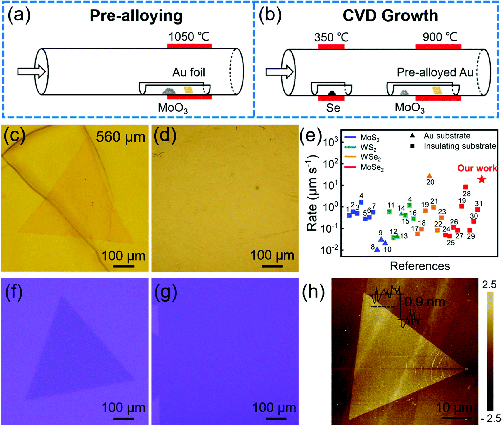 | ||
| Fig. 1 Ultrafast growth of monolayer MoSe2 single crystals and their films by pre-alloying CVD. Schematic diagram of (a) pre-alloying of Au foils and (b) ultrafast growth of submillimeter-scale monolayer MoSe2 single crystals on pre-alloyed Au foils. Optical images of (c) a 560 μm single-crystal MoSe2 and (d) a continuously uniform film. Before the MoSe2 growth, Au foil was pre-alloyed at 1050 °C for 9 times. (e) Comparison of growth rate for MX2 reported in the literature and by our method (marked by the red star). The squares and triangles in (e) represent that the substrates used for MX2 growth are insulating and Au substrates, respectively. The references numbered by 1–31 in (e) correspond to those in Table S1 (ESI†). Optical images of (f) a MoSe2 single crystal and (g) a continuous film transferred onto the SiO2/Si substrates. (h) AFM height topography of a single-crystal MoSe2 domain. The inset in (h) is the height profile measured along the black dotted line. | ||
The SEM images (Fig. S3, ESI†) show that MoSe2 single crystals can expand across the grain boundaries of polycrystalline Au foils. The morphology of MoSe2 on the different areas of the Au foils is very similar and MoSe2 domains distribute on the whole Au surface uniformly (Fig. S4, ESI†). With the growth time increasing, individual MoSe2 triangles join together to form a continuous monolayer film within 60 s (Fig. 1d). Some reports have indicated that Au foils need to be etched away for the subsequent transfer of MoS2.24–26 By contrast, as-grown MoSe2 monolayers can be successfully transferred onto SiO2/Si substrates by the electrochemical bubbling method31 (Fig. 1f, g and Fig S5, ESI†), making the pre-alloyed Au foils reusable (Fig. S6, ESI†). The thickness of the obtained MoSe2 measured by AFM (Fig. 1h) is ∼0.9 nm, illustrating its monolayer characteristic.
Structural characterization and properties of MoSe2
As shown in Fig. 2, the atomic structure of monolayer single-crystal MoSe2 was characterized by selected-area electron diffraction (SAED) and aberration-corrected scanning transmission electron microscopy (STEM). Fig. 2a shows an optical image of a single-crystal MoSe2 transferred onto a carbon supported TEM grid. The perfect coincidence of all SAED patterns (Fig. 2b) confirms that the monolayer MoSe2 is single-crystal. From the TEM image in Fig. 2c, we can see that the MoSe2 domain was clearly transferred. The energy-dispersive X-ray spectroscopy (EDS) mappings (Fig. 2d and e) were acquired at the same area in Fig. 2c, which indicates the homogeneous distribution of Mo and Se atoms in the MoSe2 flake. The stacking of monolayer MoSe2 is further observed by using atomic resolution high-angle annular dark field (HAADF) STEM. Fig. 2f is a representative HAADF-STEM image of our MoSe2, which shows a perfect hexagonal lattice structure. The distance of adjacent Se2 (Fig. 2g) and interplanar crystal spacing is 5.64 and 2.82 Å, respectively, which is consistent with the theoretical value. The atomic arrangement at the triangle edge indicates that the monolayer MoSe2 single crystal has a zigzag edge terminated with Mo atoms (Fig. 2h). These results demonstrate the good crystal quality of as-grown monolayer MoSe2 single crystals.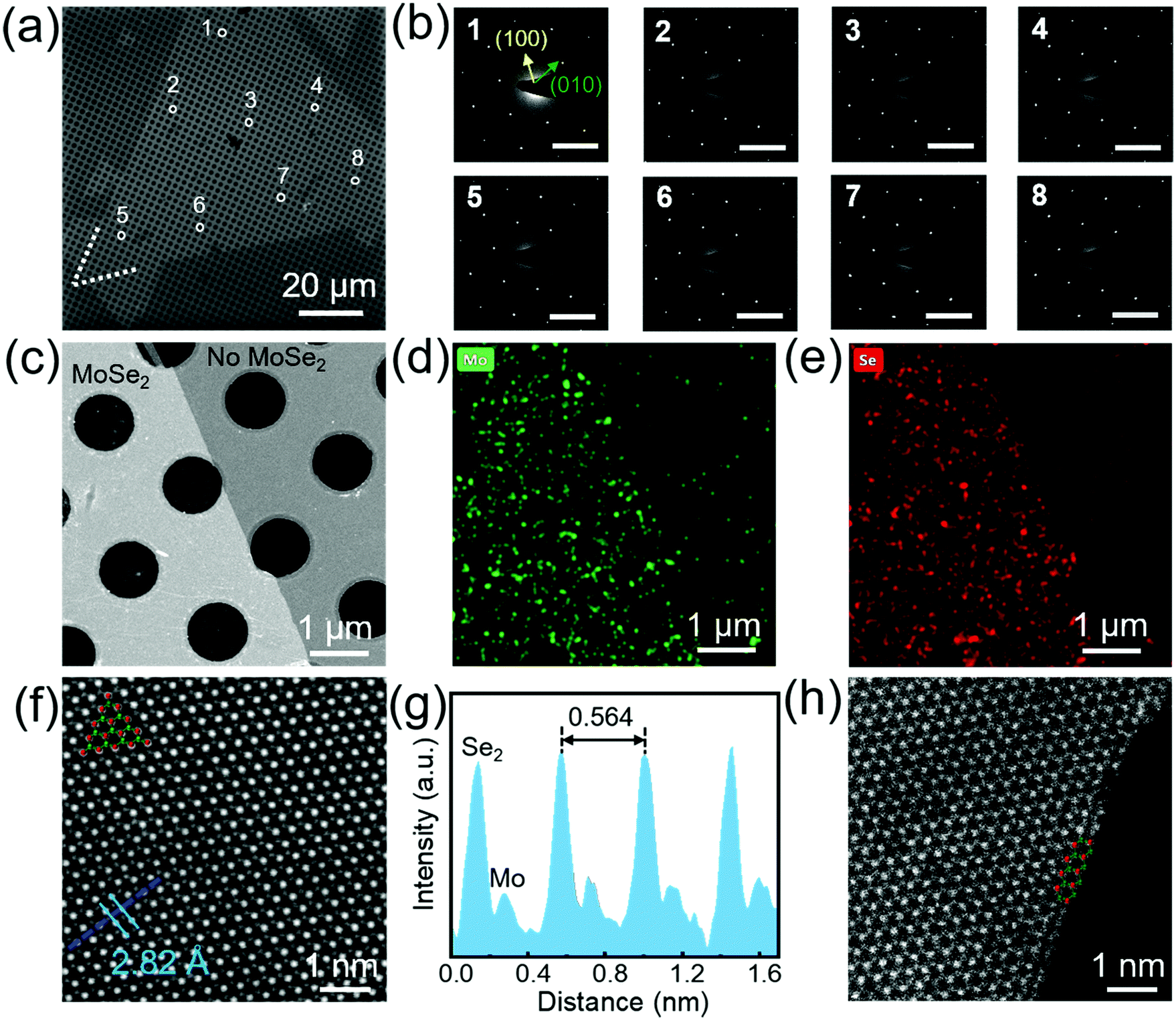 | ||
| Fig. 2 Atomic structure of monolayer MoSe2 characterized by TEM. (a) Optical image of a monolayer MoSe2 flake. (b) The 8 SAED patterns arbitrarily taken from the different regions in the same flake in (a). All scale bars are 50 nm−1. The yellow and green arrows represent lattice plane (100) and (010), respectively. (c) Low-resolution (HAADF-STEM) image of an area selected at the edge of the MoSe2 flake in (a). EDS mappings of (d) Mo and (e) Se element taken from the same area in (c). (f) Wiener filtered HAADF-STEM image of the inner area of the MoSe2 flake in (a). Due to the different atomic numbers between Se2 and Mo, the two stacked Se atoms exhibit a brighter spot than the Mo atom. (g) Element intensity profile acquired along the blue line in (f). The distance between the adjacent Se2 is 5.64 Å. (h) HAADF-STEM image of the triangle edge of the MoSe2 flake in (a). The red and green balls in (f and g) represent Se2 atoms and Mo atoms, respectively. | ||
Raman and photoluminescence (PL) spectroscopy are effective methods to characterize the crystal quality and optical properties of as-grown MoSe2. Fig. 3a–c show the optical image of transferred MoSe2 and the corresponding Raman and PL spectra. There exist two main peaks in the Raman spectra: one is a very sharp A1g mode at low wavenumber of ∼240 cm−1, representing the out-of-plane vibration. The other one is a broad E12g mode at higher wavenumber of ∼288 cm−1, representing the in-plane vibration. The A1g mode is much stronger than the E12g mode, which is a typical feature of monolayer MoSe2. The PL spectrum shows a sharp peak at ∼790 nm (A exciton) and a narrow full-width at half-maximum of ∼30 nm, corresponding to a band gap of 1.57 eV and 41 meV, respectively, which indicates that MoSe2 grown on pre-alloyed Au is a monolayer with a direct band gap. The peak position and relative intensity of the spectra in Fig. 3b and c are almost identical, suggesting that our MoSe2 domain is homogeneous. The corresponding intensity mappings of Raman and PL spectra in Fig. 3d–f further illustrate the above results. The uniformity of the large-area continuous MoSe2 film was also observed in Fig. S7 (ESI†). In addition, the electronic transport properties of MoSe2 were evaluated by fabricating a back-gate field effect transistor (FET) device (Fig. S8, ESI†). The estimated carrier mobility (11.6 cm2 V−1 s−1) is comparable to many reported TMDs (Table S1, ESI†), demonstrating the potential applications of our MoSe2 in transistors.
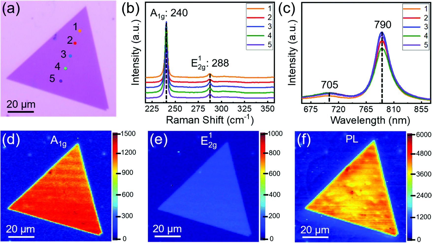 | ||
| Fig. 3 Raman and PL characterization of single-crystal MoSe2. (a) Optical image of a monolayer MoSe2 domain transferred on the SiO2/Si substrate. (b) Raman and (c) PL spectra taken from the 5 positions marked with different colours in (a), showing the characteristic peaks of MoSe2. The negligible peak in (c) at ∼705 nm is attributed to the B excitonic transition, in agreement with the reported results.27,30 The intensity mappings of (d) A1g (240 cm−1), (e) E12g (288 cm−1) and (f) PL peak (790 nm) of MoSe2 in (a). | ||
Growth mechanism of MoSe2 by pre-alloying CVD
The grain size of MoSe2 grown on original Au foils without pre-alloying was only limited to 80 μm by changing the growth temperature or precursor supply (Fig. S9, ESI†). Combining with the results in Fig. 1, we can see that pre-alloying of Au is a prerequisite to grow large-scale single-crystal MoSe2. To further evaluate the effects of pre-alloying on MoSe2 growth, we have prepared pre-alloyed Au foils with different Mo contents. Interestingly, we found that (Fig. 4a and b): with increasing the pre-alloying times, the Mo content in the pre-alloyed Au gradually increases and gets saturated after 18 times, while the grain size and nucleation density of the as-grown MoSe2 show a non-monotonic variation. To intuitively observe the relationship between the morphology evolution of MoSe2 and Mo content in pre-alloyed Au, we estimated the Mo content, grain size and nucleation density of MoSe2 with increasing pre-alloying times (Fig. 4c and d). Obviously, with the Mo content increasing, the grain size increases at first (from O to M Point), then gradually decreases (from M to S Point) and tends to be stable finally (after S Point). On the contrary, nucleation density decreases initially (from O to M Point) and then increases (from M to S Point) until it remains constant (after S Point).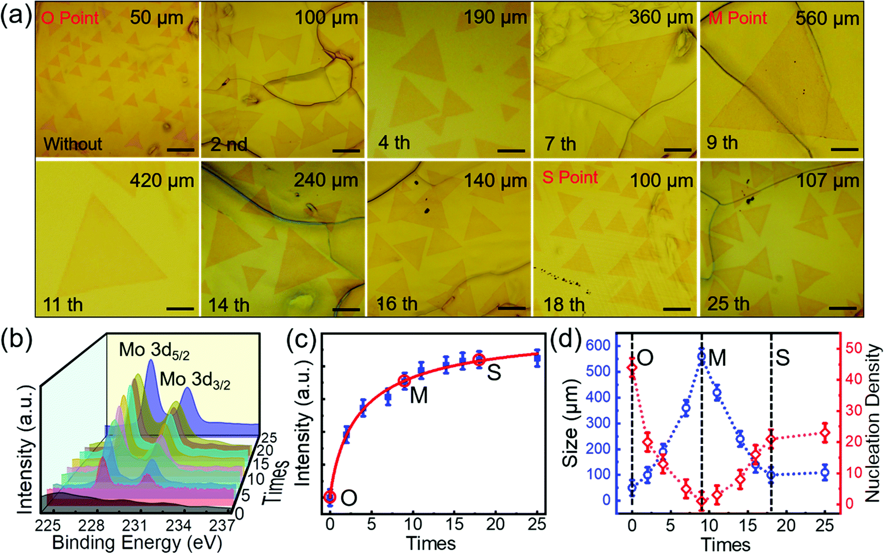 | ||
| Fig. 4 Relationship between the morphology evolution of single-crystal MoSe2 and Mo content in pre-alloyed Au. (a) A series of optical images of MoSe2 single crystals grown on the Au foils with different Mo content by pre-alloying for 0–25 times. Every pre-alloying lasts 6 min and all the MoSe2 samples were obtained in 30 s with the same CVD parameters. Scale bar in all images is 100 μm. (b) XPS spectra showing the different Mo content in pre-alloyed Au with increasing the pre-alloying times. The Mo 3d5/2 and Mo 3d3/2 peaks (238.0 eV and 231.1 eV) verify the formation of Au–Mo alloys as discussed in Fig. S2 (ESI†). (c) The variation of Mo content in Au with pre-alloying times increasing. As Mo 3d5/2 was much stronger than Mo 3d3/2, the Mo content was calculated as the peak intensity of Mo 3d5/2 in (b).36 (d) The change of nucleation density and grain size of MoSe2 in (a) with Mo content increasing. We defined the O, M and S Point as when the original Au was not pre-alloyed, the largest grain size of MoSe2 appears and the grain size keeps still, respectively. The grain counts and the side length of a triangle in (a) represent the nucleation density and grain size of MoSe2, respectively. | ||
Apparently, the Mo content in pre-alloyed Au strongly effects the MoSe2 growth. (1) Active imperfections on the metal surface, such as void sites and other defects, are favourable for nucleation of 2D materials. The passivation of these sites can effectively restrict nucleation.32–34 At the O Point, many active sites (vacancies and grain boundaries) on the original Au surface (Fig. 5a) induced the maximum nucleation density and minimum grain size of MoSe2 domains. From the O Point to M Point, the increased Mo content will gradually passivate the active sites on the Au surface, and thus the nucleation density decreases and the grain size of MoSe2 increases continuously. (2) It is worth noting that the largest grain size and smallest nucleation density appeared at the M Point (Fig. 5b), but not the S Point. Because the Mo solubility in Au decreases with the temperature decreasing according to the Au–Mo phase diagram (Fig. S10, ESI†), although the Mo content at the M point is not saturated at 1050 °C (pre-alloying temperature, ∼1.25 at%), it is saturated at the temperature for MoSe2 growth (900 °C, ∼1.11 at%). (3) After the M Point, redundant Mo atoms precipitate onto the Au surface more and more (Fig. S11, ESI†). Although the pre-deposited Mo can act as a Mo source for MoSe2 growth, it has a slight effect on promoting the grain size (Fig. S12, ESI†). The excess Mo atoms will provide active sites and accelerate the MoSe2 nucleation (Fig. 5c).35 As a result, the grain size of MoSe2 decreased from the M Point to the S Point.
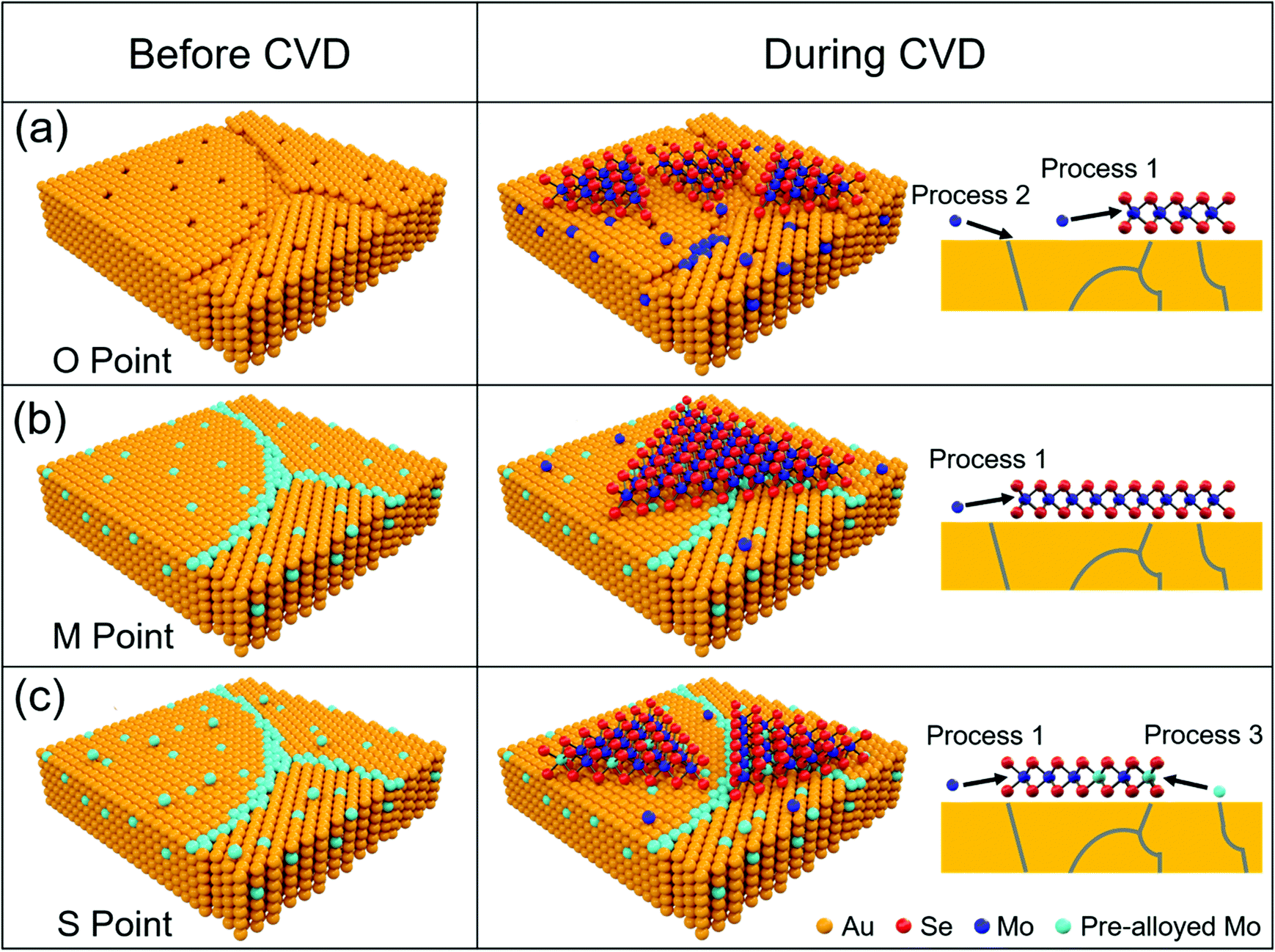 | ||
| Fig. 5 Schematic of MoSe2 growth on pre-alloyed Au with different Mo content. (a) The original polycrystalline Au surface with many defects, including vacancies and grain boundaries (O Point in Fig. 4). Au–Mo alloys appeared (Process 2) and MoSe2 formed (Process 1) simultaneously with the Mo source supply introduced by a carrier gas, which makes a strong interaction between MoSe2 and Au. (b) Mo content got saturated at 900 °C. Actively defective sites on the Au surface were totally passivated by Mo atoms (M Point in Fig. 4), which induced the minimum nucleation density of MoSe2 and a weak interaction between MoSe2 and Au. (c) Mo was oversaturated at 900 °C (S Point in Fig. 4). Excess Mo atoms diffused onto the Au surface, which provide the new nucleation sites and increase the nucleation density of MoSe2 (Process 3). Mo atoms coming from pre-alloyed Au are coloured by light blue, while those introduced during MoSe2 growth are coloured by dark blue. The schematic of Au was built based on the cross section of pre-alloyed Au foils (Fig. S13, ESI†). | ||
In addition, we found that pre-alloying not only suppressed the nucleation density by passivating the active sites on the Au surface but also induced a weak interaction between MoSe2 and Au, which makes the following transfer easy. When MoSe2 was synthesized on original Au without pre-alloying, Mo atoms occupy the void sites of the Au surface and react with Se simultaneously to form a Se–Mo–Au structure.37 This phenomenon will greatly enhance the interaction between Au and MoSe2. By contrast, void sites and other defects of the Au surface can be passivated in advance by pre-alloying CVD (M Point in Fig. 5). In this way, the main Mo source for MoSe2 growth comes from Mo introduced by carrier gas but not pre-deposited Mo in Au (Fig. S12, ESI†). We think that such a growth process is similar to the reported surface catalytic growth of WS2 or WSe2 on Au,10,19 which may induce a weak interaction between MoSe2 and Au (Fig. S14, ESI†). As a result, the MoSe2 domains obtained at the O Point were seriously damaged, while those grown on pre-alloyed Au (M and S Point) were completely transferred (Fig. S15, ESI†).
Except for the low nucleation density, high growth rate also gets involved in the formation of submillimeter-scale single-crystal MoSe2. As reported, MoS2 can be synthesized in pure Ar,33 but MoSe2 domains only appeared when H2 was introduced in our experiments. H2 acted as both a reduction promoter for the adequate selenylation of MoO3 and an etching agent of as-grown MoSe2. The growth rate was intensively influenced by the H2 concentration. Introducing a moderate amount of H2 (3 sccm) will speed up the growth of uniform monolayer MoSe2 without any multilayer (Fig. S16, ESI†).
Fast growth of large-scale single-crystal MoS2
We have also confirmed that pre-alloying CVD is also applicable for the fast growth and non-destructive transfer of other 2D TMDs (Fig. S17 and S18, ESI†). As reported, the growth rate of MoS2 on Au is very low (∼0.03 μm s−1) and Au foils need to be etched away for transferring MoS2.24–26 By contrast, ∼450 μm-sized triangular MoS2 was formed within 2 min by pre-alloying CVD. Although the growth rate of MoS2 (∼3.75 μm s−1) is much lower than MoSe2 (details discussed in Fig. S17, ESI†), it is still over 100 times higher than reported results, as shown in Table S2 (ESI†). Furthermore, Au foils were reusable and MoS2 can be completely transferred.Conclusions
In conclusion, the ultrafast growth of submillimeter-scale monolayer single-crystal MoSe2 was realized by pre-alloying CVD. The uniform high-quality MoSe2 monolayers can be successfully transferred without sacrificing Au foils by using the electrochemical bubbling method. We further revealed the significant role of pre-alloying in the ultrafast growth of MoSe2. It can not only suppress the nucleation density by passivating the active sites on the Au surface, but also induce a weak interaction between MoSe2 and Au, which makes the following transfer easy. This method is also universal for the fast growth and non-destructive transfer of other 2D TMDs. Pre-alloying CVD offers important insights for the synthesis of large-scale high-quality TMDs and other 2D materials, which paves the way for their electronic and optoelectronic applications.Author contributions
Conceptualization: X. Xin, H. Xu and W. Ren; Investigation: X. Xin, J. Chen, Y. Zhan, Y. Bao and M.-L. Chen; Funding acquisition: X. Xin, H. Xu, W. Liu, Y. Liu and W. Ren. Writing: X. Xin, J. Chen, H. Xu and W. Ren.Conflicts of interest
There are no conflicts to declare.Acknowledgements
This work was supported by the National Science Fund for Distinguished Young Scholars (No. 52025022), the Program of National Natural Science Foundation of China (No. 52002056, 11874104, 12074060, 51872043, U19A2091 and 51732003), the Chinese Academy of Sciences (No. XDB30000000 and ZDBS-LY-JSC027), the National Key Research and Development Program of China (No. 2021YFA0716400 and 2019YFB2205100), the Fundamental Research Funds for the Central Universities (No. 2412020QD014, 2412021ZD006, 2412019BJ006 and 2412021ZD012), the fund from Jilin Province (No. YDZJ202101ZYTS046, YDZJ202101ZYTS133 and JJKH20211273KJ) and LiaoNing Revitalization Talents Program (No. XLYC1808013).References
- K. F. Mak and J. Shan, Nat. Photonics, 2016, 10, 216–226 CrossRef CAS.
- J. Gu, B. Chakraborty, M. Khatoniar and V. M. Menon, Nat. Nanotechnol., 2019, 14, 1024–1028 CrossRef CAS PubMed.
- N. Li, Q. Wang, C. Shen, Z. Wei, H. Yu, J. Zhao, X. Lu, G. Wang, C. He, L. Xie, J. Zhu, L. Du, R. Yang, D. Shi and G. Zhang, Nat. Electron., 2020, 3, 711–717 CrossRef CAS.
- Z. D. Luo, X. Xia, M. M. Yang, N. R. Wilson, A. Gruverman and M. Alexe, ACS Nano, 2020, 14, 746–754 CrossRef CAS PubMed.
- M. Kim, J. Seo, J. Kim, J. S. Moon, J. Lee, J. H. Kim, J. Kang and H. Park, ACS Nano, 2021, 15, 3038–3046 CrossRef CAS PubMed.
- A. M. van der Zande, P. Y. Huang, D. A. Chenet, T. C. Berkelbach, Y. You, G. H. Lee, T. F. Heinz, D. R. Reichman, D. A. Muller and J. C. Hone, Nat. Mater., 2013, 12, 554 CrossRef CAS PubMed.
- S. Najmaei, Z. Liu, W. Zhou, X. Zou, G. Shi, S. Lei, B. I. Yakobson, J. C. Idrobo, P. M. Ajayan and J. Lou, Nat. Mater., 2013, 12, 754 CrossRef CAS PubMed.
- V. S. Calderon, R. V. Ferreira, D. Taneja, R. T. Jayanth, L. Zhou, R. M. Ribeiro, D. Akinwande and P. J. Ferreira, Nano Lett., 2021, 21, 10157–10164 CrossRef PubMed.
- S. S. Wu, T. X. Huang, X. Xu, Y. F. Bao, X. D. Pei, X. Yao, M. F. Cao, K. Q. Lin, X. Wang, D. Wang and B. Ren, ACS Nano, 2022, 16, 4786–4794 CrossRef CAS PubMed.
- Y. Gao, Y. L. Hong, L. C. Yin, Z. Wu, Z. Yang, M. L. Chen, Z. B. Liu, T. Ma, D. M. Sun, Z. H. Ni, X. L. Ma, H. M. Cheng and W. Ren, Adv. Mater., 2017, 29, 1700990 CrossRef PubMed.
- J. Zhou, J. Lin, X. Huang, Y. Zhou, Y. Chen, J. Xia, H. Wang, Y. Xie, H. Yu, J. Lei, D. Wu, F. Liu, Q. Fu, Q. Zeng, C.-H. Hsu, C. Yang, L. Lu, T. Yu, Z. Shen, H. Lin, B. I. Yakobson, Q. Liu, K. Suenaga, G. Liu and Z. Liu, Nature, 2018, 556, 355–359 CrossRef CAS PubMed.
- X. Xu, Z. Zhang, L. Qiu, J. Zhuang, L. Zhang, H. Wang, C. Liao, H. Song, R. Qiao, P. Gao, Z. Hu, L. Liao, Z. Liao, D. Yu, E. Wang, F. Ding, H. Peng and K. Liu, Nat. Nanotechnol., 2016, 11, 930–935 CrossRef CAS PubMed.
- M. C. Chang, P. H. Ho, M. F. Tseng, F. Y. Lin, C. H. Hou, I. K. Lin, H. Wang, P. P. Huang, C. H. Chiang, Y. C. Yang, I. T. Wang, H. Y. Du, C. Y. Wen, J. J. Shyue, C. W. Chen, K. H. Chen, P. W. Chiu and L. C. Chen, Nat. Commun., 2020, 11, 3682 CrossRef CAS PubMed.
- Q. Ji, Y. Zhang, T. Gao, Y. Zhang, D. Ma, M. Liu, Y. Chen, X. Qiao, P. H. Tan, M. Kan, J. Feng, Q. Sun and Z. Liu, Nano Lett., 2013, 13, 3870–3877 CrossRef CAS PubMed.
- A. L. Elías, N. Perea-López, A. Castro-Beltrán, A. Berkdemir, R. Lv, S. Feng, A. D. Long, T. Hayashi, Y. A. Kim, M. Endo, H. R. Gutiérrez, N. R. Pradhan, L. Balicas, T. E. Mallouk, F. López-Urías, H. Terrones and M. Terrones, ACS Nano, 2013, 7, 5235–5242 CrossRef PubMed.
- Y. Zhang, Y. Zhang, Q. Ji, J. Ju, H. T. Yuan, J. Shi, T. Gao, D. Ma, M. Liu, Y. Chen, X. Song, H. Y. Hwang, Y. Cui and Z. Liu, ACS Nano, 2013, 7, 8963–8971 CrossRef CAS PubMed.
- Y. H. Lee, L. Yu, H. Wang, W. Fang, X. Ling, Y. Shi, C. T. Lin, J. K. Huang, M. T. Chang, C. S. Chang, M. Dresselhaus, T. Palacios, L. J. Li and J. Kong, Nano Lett., 2013, 13, 1852–1857 CrossRef CAS PubMed.
- S. J. Yun, S. H. Chae, H. Kim, J. C. Park, J. H. Park, G. H. Han, J. S. Lee, S. M. Kim, H. M. Oh, J. Seok, M. S. Jeong, K. K. Kim and Y. H. Lee, ACS Nano, 2015, 9, 5510–5519 CrossRef CAS PubMed.
- Y. Gao, Z. Liu, D. M. Sun, L. Huang, L. P. Ma, L. C. Yin, T. Ma, Z. Zhang, X. L. Ma, L. M. Peng, H. M. Cheng and W. Ren, Nat. Commun., 2015, 6, 8569 CrossRef CAS PubMed.
- P. Yang, S. Zhang, S. Pan, B. Tang, Y. Liang, X. Zhao, Z. Zhang, J. Shi, Y. Huan, Y. Shi, S. J. Pennycook, Z. Ren, G. Zhang, Q. Chen, X. Zou, Z. Liu and Y. Zhang, ACS Nano, 2020, 14, 5036–5045 CrossRef CAS PubMed.
- S. H. Choi, H. J. Kim, B. Song, Y. I. Kim, G. Han, H. T. T. Nguyen, H. Ko, S. Boandoh, J. H. Choi, C. S. Oh, H. J. Cho, J. W. Jin, Y. S. Won, B. H. Lee, S. J. Yun, B. G. Shin, H. Y. Jeong, Y. M. Kim, Y. K. Han, Y. H. Lee, S. M. Kim and K. K. Kim, Adv. Mater., 2021, 33, 2006601 CrossRef CAS PubMed.
- H. Okamoto and T. B. Massalski, Bull. Alloy Phase Diagrams, 1985, 6, 136–137 CrossRef CAS.
- T. B. Massalski, H. Okamoto and L. Brewer, Bull. Alloy Phase Diagrams, 1986, 7, 449–452 CrossRef CAS.
- J. Shi, X. Zhang, D. Ma, J. Zhu, Y. Zhang, Z. Guo, Y. Yao, Q. Ji, X. Song, Y. Zhang, C. Li, Z. Liu, W. Zhu and Y. Zhang, ACS Nano, 2015, 9, 4017–4025 CrossRef CAS PubMed.
- J. Shi, D. Ma, G. F. Han, Y. Zhang, Q. Ji, T. Gao, J. Sun, X. Song, C. Li, Y. Zhang, X. Y. Lang, Y. Zhang and Z. Liu, ACS Nano, 2014, 8, 10196–10204 CrossRef CAS PubMed.
- J. Shi, Y. Yang, Y. Zhang, D. Ma, W. Wei, Q. Ji, Y. Zhang, X. Song, T. Gao, C. Li, X. Bao, Z. Liu, Q. Fu and Y. Zhang, Adv. Funct. Mater., 2015, 25, 842–849 CrossRef CAS.
- J. S. Ross, S. Wu, H. Yu, N. J. Ghimire, A. M. Jones, G. Aivazian, J. Yan, D. G. Mandrus, D. Xiao, W. Yao and X. Xu, Nat. Commun., 2013, 4, 1474 CrossRef PubMed.
- X. Wang, Y. Gong, G. Shi, W. L. Chow, K. Keyshar, G. Ye, R. Vajtai, J. Lou, Z. Liu, E. Ringe, B. K. Tay and P. M. Ajayan, ACS Nano, 2014, 8, 5125–5131 CrossRef CAS PubMed.
- S. Tongay, J. Zhou, C. Ataca, K. Lo, T. S. Matthews, J. Li, J. C. Grossman and J. Wu, Nano Lett., 2012, 12, 5576–5580 CrossRef CAS PubMed.
- G. W. Shim, K. Yoo, S. B. Seo, J. Shin, D. Y. Jung, I. S. Kang, C. W. Ahn, B. J. Cho and S. Y. Choi, ACS Nano, 2014, 8, 6655–6662 CrossRef CAS PubMed.
- L. Gao, W. Ren, H. Xu, L. Jin, Z. Wang, T. Ma, L. P. Ma, Z. Zhang, Q. Fu, L. M. Peng, X. Bao and H. M. Cheng, Nat. Commun., 2012, 3, 699 CrossRef PubMed.
- Y. Hao, M. S. Bharathi, L. Wang, Y. Liu, H. Chen, S. Nie, X. Wang, H. Chou, C. Tan, B. Fallahazad, H. Ramanarayan, C. W. Magnuson, E. Tutuc, B. I. Yakobson, K. F. McCarty, Y. W. Zhang, P. Kim, J. Hone, L. Colombo and R. S. Ruoff, Science, 2013, 342, 720–723 CrossRef CAS PubMed.
- J. Chen, X. Zhao, S. J. R. Tan, H. Xu, B. Wu, B. Liu, D. Y. Fu, W. Fu, D. Geng, Y. Liu, W. Liu, W. Tang, L. Li, W. Zhou, T. C. Sum and K. P. Loh, J. Am. Chem. Soc., 2017, 139, 1073–1076 CrossRef CAS PubMed.
- H. Zhou, W. J. Yu, L. Liu, R. Cheng, Y. Chen, X. Huang, Y. Liu, Y. Wang, Y. Huang and X. Duan, Nat. Commun., 2013, 4, 2096 CrossRef PubMed.
- P. Shao, L. P. Ding and F. Ding, Chem. Mater., 2021, 33, 3241–3248 CrossRef CAS.
- V. Kiran, D. Mukherjee, R. N. Jenjeti and S. Sampath, Nanoscale, 2014, 6, 12856–12863 RSC.
- F. Cheng, Z. X. Hu, H. Xu, Y. Shao, J. Su, Z. Chen, W. Ji and K. P. Loh, ACS Nano, 2019, 13, 2316–2323 CAS.
Footnotes |
| † Electronic supplementary information (ESI) available. See DOI: https://doi.org/10.1039/d2nh00105e |
| ‡ Equal contribution. |
| This journal is © The Royal Society of Chemistry 2022 |