DOI:
10.1039/D2NH00015F
(Communication)
Nanoscale Horiz., 2022,
7, 1228-1239
Optical response of hyperbolic metamaterials with adsorbed nanoparticle arrays†
Received
12th January 2022
, Accepted 5th July 2022
First published on 15th August 2022
Abstract
Experimental studies of have been recently performed to determine the optical effect of adsorption of arrays of gold nanoparticles, NPs (16 nm or 40 nm in diameter) on reflective substrates (Ma et al., ACS Photonics, 2018, 5, 4604–4616; Ma et al., ACS Nano, 2020, 14, 328–336) and on transparent interfaces (Montelongo et al., Nat. Mater., 2017, 16, 1127–1135). As predicted by the theory (Sikdar et al., Phys. Chem. Chem. Phys., 2016, 18, 20486–20498), a reflection quenching effect was observed on the reflective substrates, in the frequency domain centred around the nanoparticle localised plasmon resonance. Those results showed a broad dip in reflectivity, which was deepening and red-shifting with increasing array densities. In contrast, the second system has shown, also in accordance with the theory (Sikdar and Kornyshev, Sci. Rep., 2016, 6, 1–16), a broad reflectivity peak in the same frequency domain, increasing in intensity and shifting to the red with densification of the array. In the present paper, we develop a theory of an optical response of NP arrays adsorbed on the surface of stacked nanosheet hyperbolic substrates. The response varies between quenched and enhanced reflectivity, depending on the volume fractions of the metallic and dielectric components in the hyperbolic metamaterial. We reproduce the results of the earlier works in the two opposite limiting cases – of a pure metal and a pure dielectric substrates, while predicting novel resonances for intermediate compositions. Whereas the metal/dielectric ratio in the hyperbolic substrate cannot be changed in time – for each experiment a new substrate should be fabricated – the density of the adsorbed nanoparticle arrays can be controlled in real time in electrochemical photonic cells (Montelongo et al., Nat. Mater., 2017, 16, 1127–1135; Ma et al., ACS Photonics, 2018, 5, 4604–4616; Ma et al., ACS Nano, 2020, 14, 328–336). Therefore, we systematically study the effect of the array density on the optical response of such systems, which could be later verified experimentally. We also investigate the manifestation of these findings in a hyperbolic-Fabry-Perot cell.
New concepts
There was recently a great interest in creation of tuneable, reconfigurable nanophotonic structures. Whereas the chemistry of ordinary materials operates with atoms and molecules as building blocks, novel photonic metamaterials are designed using subwavelength scale building blocks, enabling enhanced/exotic optical effects. But most of those materials are static. Can we create systems reconstructable in real time, momentarily changing their optical properties at will? A breakthrough towards this goal came from electrochemical cells where adsorption/desorption of plasmonic nanoparticles can be induced and controlled with 1 V variation of applied voltage. This was achieved on either purely transparent (liquid–liquid) or purely reflective (metallic) electrodes. In this communication we show that we can get a much broader range of opportunities if we consider electrodes made of layered composite hyperbolic metamaterials. A variety of spectra emerge for different densities of the nanoparticle arrays, opening the window for novel applications of such systems. One of them is light capture and filtering with Fabry–Perot cavities, enclosed by such electrodes. The hyperbolic metamaterial allows the enhancement of some transmission peaks, at the frequencies of interest, at the expense of others. Additionally, voltage controlled electrosorption of nanoparticles on electrode surfaces fine-tunes the intensity of these peaks as needed.
|
1. Introduction
Optical systems based on plasmonic nanoparticles (NPs) have shown tremendous potential in photonics due to their ability to provide self-assembling electrotunable nanostructures.1,2 More specifically, the reliability and reproducibility of the optical signals (especially reflectance and transmittance) has withstood both theoretical and experimental scrutiny.1–6 The key idea here was to stimulate spontaneous assembly of charged NPs into two dimensional arrays, located at electrochemical interfaces and control the resulting array density by applied voltage, fine tuning this by solution pH and electrolyte concentration.1,2,6 The balance between NP-interface attraction (due mostly to the applied electric field) and NP-NP electrostatic repulsion due to residual negative charges of dissociated terminal acidic groups, allows establishing the optimal NP density on the surface packing into almost ideal hexagonal arrays.
Both dielectric–dielectric1 and dielectric–metal2 interfaces have been examined theoretically and experimentally, each interface showing qualitatively distinct optical signals. Generally, light is able to induce localized surface plasmons in every single NP.5,7 Assembling the particles into a two-dimensional array will allow in-plane coupling of the localised plasmons, resulting in a strong interaction with light.8 In the case of a dielectric substrate the plasmon coupling will result in a highly reflective surface, resembling a mirror.1,9 On the other hand, light interaction with a metallic substrate in the presence of NPs, will excite surface plasmons at the interface, which will couple with the localised plasmons of the NP array, resulting in the enhanced absorption of specific light frequencies, due to the resonance coupling between localised and surface plasmons.10 The overall optical effect is thus the quenching of a broad band of wavelengths, centred around the localised plasmon resonance frequency.2
With the unravelled prospect of enhancing or quenching reflectance, we may now ask ourselves, whether we can design a system that could enhance certain wavelengths while quenching others. In order to achieve this, the substrate would have to qualitatively behave both as a dielectric and metal, depending on the light frequency range where these effects are desired. As of yet, there are very few materials that could show such a dramatic change in behaviour with wavelength. One typical example is graphene, which exhibits transparent dielectric behaviour in the visible range, while the far infrared is dominated by the so-called hyperbolic behaviour.11,12 Alternatively, such variation of optical properties can be generated using sub-wavelength metal-dielectric structures in order to achieve the transition from metallic to dielectric-like response, within the visible range. These structures are known in literature as Hyperbolic metamaterials (HMM).13,14
There were theoretical and experimental studies of HMMs with rough surfaces as light absorbers and scatterers15–17 and investigations of the effects of individual NPs15 or NP arrays18 on top of HMM to boost light absorption. Some of the structures involving HMMs do not involve NPs, but they do, nonetheless, exhibit incredibly strong light absorption, both in the visible and infrared regions,19–21 and have been already used in various applications, e.g. enhancement and control of photoluminescence,22 plasmonic lithography with an ambition to surpass the diffraction limit,23 transformation of evanescent waves into propagating waves and development of hyperlenses.24 Some papers have studied the optical response of a lone NP on an HMM.25–27 The results that we present here are centred on different effects. Unlike the previous studies focussing on absorbed and scattered powers, in this study we are interested in the detailed pattern of reflection spectra. The presented version of the effective medium theory (which accounts, in particular, for image effects), altogether checked against simulations, unravels these patterns. We find that depending on the composition of HMM substrate and the density of the adsorbed NP array, dramatic changes in the reflection spectra may occur, ranging from a broad band reflection to almost 100% reflection quenching. Those effects could be utilized on isolated surfaces or in Fabry–Perot cavities, and most importantly in electrochemical photonic cells in which the density of the NP arrays can be controlled by tiny variation (within 1 V) of applied voltage. From that point of view the main goal of this article is to provide a platform that will navigate future experimental realization of such novel systems.
2. Hyperbolics substrates and how we will treat them
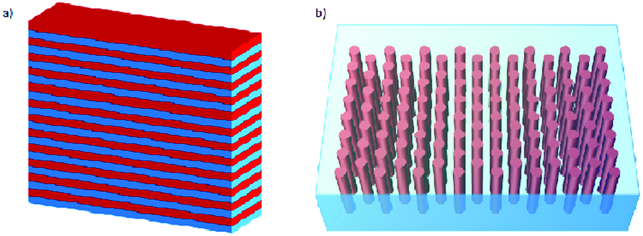
HMMs come in a variety of different geometries. However, there are only two simple structures typically considered for theoretical investigations: one consists of nanowires embedded into a dielectric matrix while the other (considered in this paper) consists of stacked metal and dielectric nanosheets, in an alternating pattern.13,14,28–31 There are also more complex nanostructures, where the geometry of the material dictates how the electromagnetic field behaves inside those materials.32–34 Both of the structures are shown in Fig. 1, but in this paper we will focus on the sheet structures.
 |
| | Fig. 1 Most common HMM structures used in theoretical investigations: (a) stacked nanosheet structure and (b) embedded nanowire structure. The former is being considered in the present work. | |
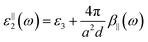
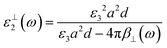
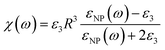
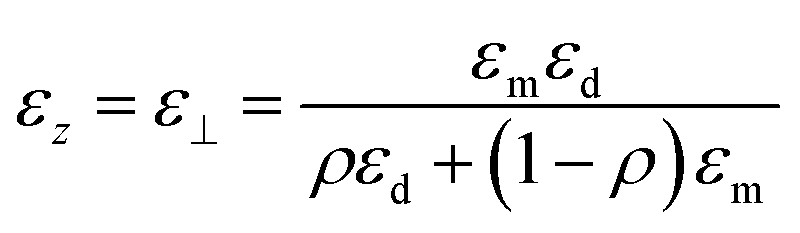
The structural of these materials gives rise to an anisotropy in their dielectric tensor. Due to the thickness of the sheets being smaller than the wavelength of light, the HMM can be treated theoretically as an effective material, where the components of the dielectric tensor can be approximated using the generalized Maxwell–Garnett model.13,14 More specifically, the first two diagonal elements will be identical (ε‖) while the third element will be different (ε⊥), given respectively by eqn (1) and (2).13,14
| | | εx = εy = ε‖ = ρεm + (1 − ρ)εd | (1) |
| | 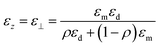 | (2) |
here,
εm and
εd are the dielectric constants of the metal and the dielectric respectively and
ρ is the ‘fill fraction’ (metal volume fraction in the HMM). As the dielectric tensors change at different rates with wavelength, different behaviours are observed as follows:
35
• When both ε⊥ < 0 and ε‖ < 0, the HMM behaves as a metal.
• When ε⊥ > 0 and ε‖ > 0, the HMM behaves as a dielectric.
• When ε⊥ < 0 and ε‖ > 0, the HMM behaves as a Type I material, causing the HMM to behave as a metal in response to the projection of electric field in the direction perpendicular to the interface and an effective dielectric with respect to the component of the field in the plane parallel to the interface.
• Where ε⊥ > 0 and ε‖ < 0, the HMM behaves as a Type II material, causing the HMM to behave as a dielectric in the direction normal to the interface and a metal in the plane parallel to it.
Note that HMMs that we will consider here will manifest themselves as a Type 1 material at low wavelengths and Type 2 material at high wavelengths. Thus, with the considered nanosheet structures, we will encounter with the performance of HMM in both Type 1 and Type 2 modes, depending on the wavelength of light.
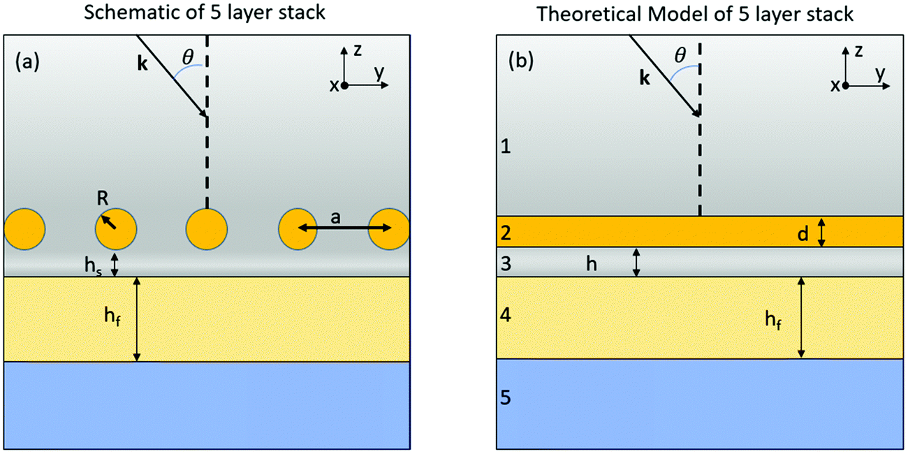
In the systems considered previously,1–5 the substrate was isotropic. Thus, earlier developed theory of the optical response had to be modified here in order to account for the subtleties of interaction of the localised plasmons in the NP arrays with an anisotropic substrate. The description of the NP array can still be based on the Effective Medium Theory (EMT),4,5 which models the NP array as a slab with effective in-plane and out-of-plane dielectric functions, as seen in Fig. 2, with a tricky overall anisotropic effective dielectric function, depending in the first place on the properties of materials of NPs, their size, and the array density. The basics of the model are laid out in ref. 4 and 5, and in the present work we focused on extending that theoretical framework to account for anisotropy of the dielectric response of the substrate. Now the light wavevector passing the HMM layer would have to be split into a parallel and perpendicular component and the images of induced dipoles in each NP (their polarizability is considered in dipole approximation) in the HMM would have to be recalculated accordingly. The approach relies on the same approximation as the Maxwell–Garnet model, and, thus, the discrete nature of the HMM structure is incorporated into the theory of dielectric response in an effective manner, but is not considered explicitly.
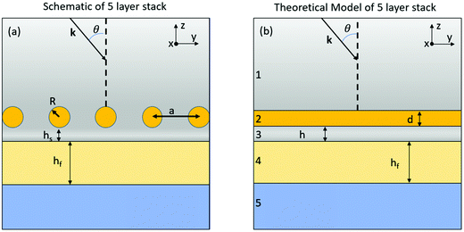 |
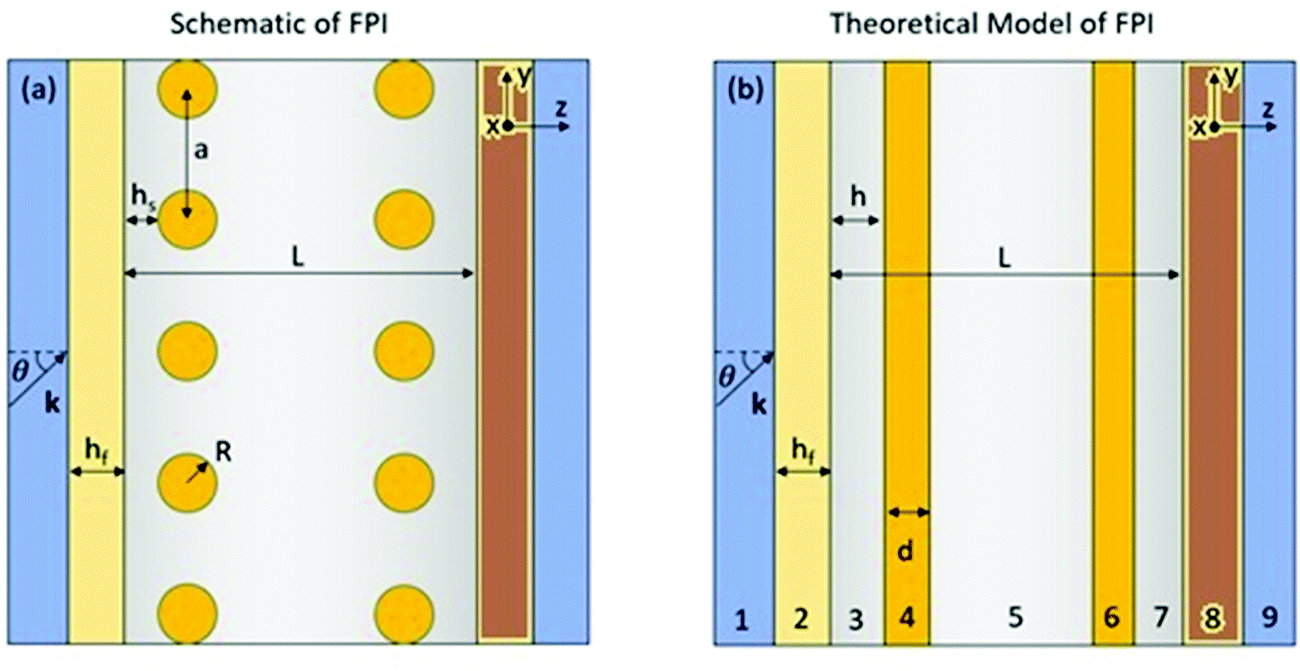
| | Fig. 2 5-Layer stack model. (a) The sketched profile of the system of a nanoparticle array with a lattice constant “a” on top of a bilayer substrate. (b) The Schematic of the 5-layer stack model representing this system. The incident light propagates through layer 1 (transparent semi-infinite medium) with a wavevector k and angle of incidence θ. Layer 2 of effective thickness d represents the NP array; its effective polarizability is calculated from the effective medium theory (as described in the text). Layer 3 is the spacer layer of thickness h, reflecting the hs-separation of NPs in panel (a) from the HMM slab (layer 4) of thickness hf. Layer 5 is a semi-infinite transparent material (glass or transparent electrode, such as TiO2 or ZnO) the system is mounted on. How hs is mapped on h is described in the text. | |
Since all ligand-functionalized NPs are located very close to the substrate (only one or few nm away), a potential improvement of the model would be to treat the first nanosheet as a separate layer, thus splitting the layer 4 in Fig. 2 in two unequal sheets. Experimentally, the top-sheet should be a dielectric one, to protect the hyperbolic electrode against corrosion or any other unwanted electrochemical activity. The rest of the layer 4 (Fig. 2) can still be considered as ‘uniform’ anisotropic medium. This possibility, as well as the consequences of such splitting, will be discussed in the ESI;† it produces the same qualitative result as the model which does not involve such splitting, but it does it more accurately, when compared with COMSOL, namely with full wave simulations designed to test the EMT. Details on the simulations are provided in the ESI.†
3. The model
The NPs are considered to form a layer above the interface between the HMM and the Bulk dielectric, as sketched in the left panel of Fig. 2. In the EMT the whole system is represented by 5 layers, with layer 1 being transparent dielectric (electrolyte); layer 3 acting as a separator of thickness hs between layers 2 and 4; layer 2 is the one representing an array of NPs, with an effective thickness d, layer 4 is the HMM of thickness hf and layer 5 is the material on which the system is mounted, which is treated as a semi-infinite transparent half space. The separator (layer 3) whose thickness is denoted by hs typically arises from the ligand coating used when NP solutions are prepared. As a result, hs is usually of the order of a 1–3 nm. If we deal with metal core-dielectric shell NPs, hs could get larger, e.g. 5–10 nm. For a moderate increase of hs, the observed spectra will slightly change to the blue due to weaker interactions between the excited dipoles of NPs and their images. When hs gets increased in this way to above 100 nm, the effects will be completely different; when hs becomes comparable to the wavelength of light, Fabry Perot effects will come into play. We are not considering this situation in our paper, but in its final part we perform a case study of a specially designed Fabry–Perot cell which involves the HMM as one of its confining plates.
The assumption used here is that the HMM behaves as an effective material, with no internal fine structure present, as well as the dipole images not ‘travelling’ beyond the HMM. Compared to the previous model (4-layer stack), the HMM is not an isotropic layer, unlike the semi-infinite metallic substrate of the NP-on-mirror system. In HMM (layer 4), the wavevector has to be split into a parallel and perpendicular component (k4,‖ and k4,⊥), in order to account for the anisotropic dielectric tensor of the HMM. The more interesting difference, however, arises from the implementation of interaction between the NP dipolar modes and their images. The description of the latter has to start with the derivation of the electrostatic Green's function for a point charge in front of an anisotropic semi-infinite material.
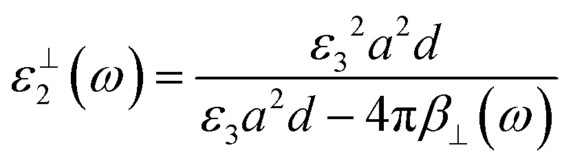
The effective permittivity of the NP layer in the parallel and perpendicular directions is calculated viaeqn (3) and (4) respectively.
| |  | (3) |
| |  | (4) |
The NPs are embedded in the bulk dielectric forming a quasi-static 2D array, where
ε3 is the permittivity of the bulk dielectric;
a is the lattice constant of the NP structure,
β‖(
ω)(
β⊥(
ω)) is the effective polarizability of the average NP in the parallel (perpendicular) direction, and
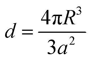
d is the characteristic thickness of the effective NP layer. The effective polarizability of the NP also accounts for the interaction of the individual NPs with every other NP and their images using the dipole approximation. The characteristic thickness of the NP layer is taken as:
| |  | (5) |
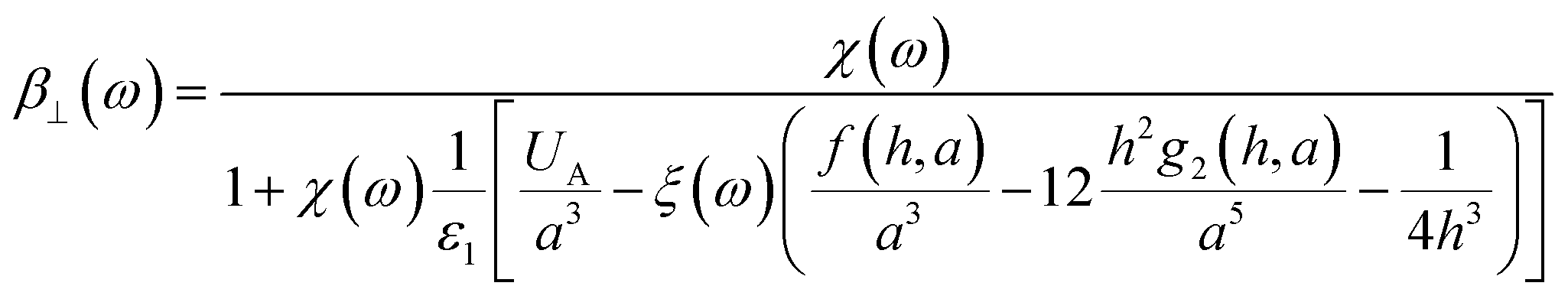
For the 5 Layer stack model the effective polarizability of each NP in the array is given by
eqn (6) and (7) in the parallel and perpendicular directions.
| | 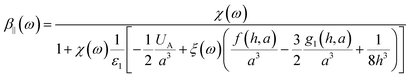 | (6) |
| | 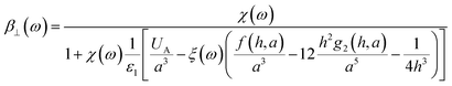 | (7) |
where
χ(
ω) is the frequency dependent polarizability of the individual spherical NP,
ξ is the quasi-static image charge screening factor and
UA,
f(
h,
a),
g1(
h,
a),
g2(
h,
a) are the lattice dependent parameters, which we will specify below. The polarizability of each NP with radius
R ≪
λ, the wave-length of light, is given by:
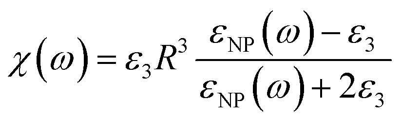
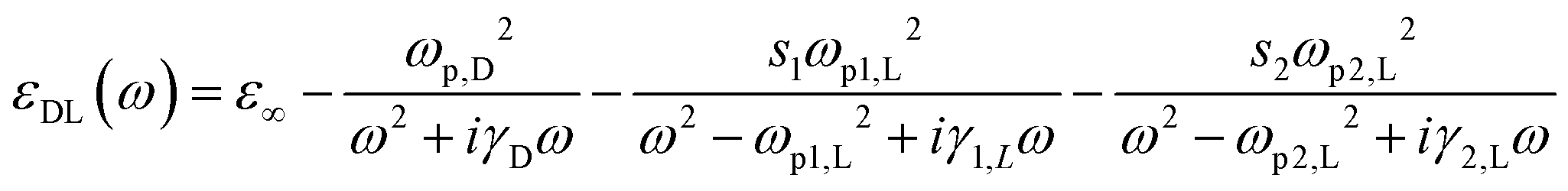
| |  | (8) |
here
εNP(
ω) is the dielectric constant of the material of the NP as determined through the Drude–Lorenz approximation,
3 as given in
eqn (9), which takes into account in addition to the plasmon mode, the effect of the inter band transitions in the form of two Lorentzians:
| | 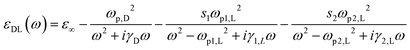 | (9) |
where
ε∞ is the permittivity of the material at high frequencies. The second term comes from the Drude model, with
ωp,D being the plasma frequency and
γD being the plasma damping coefficient. The third and fourth terms come from the Lorentzian extension to the Drude model, with the
ωp1,L and
ωp2,L being the resonance frequencies,
γ1,L and
γ2,L being the spectral widths of those two resonances;
s1 and
s2 are the weighing factors and
ω is the frequency being looked at. The parameters which we will be using in this paper, are shown in
Table 1.
Table 1 The parameters for the Drude–Lorentz model for gold and silver
|
|
ε
∞
|
ω
p,D (eV) |
γ
D (eV) |
s
1
|
ω
p1,L (eV) |
γ
1,L (eV) |
s
2
|
ω
p2,L (eV) |
γ
2,L (eV) |
| Gold |
5.9752 |
8.8667 |
0.03799 |
1.76 |
3.6 |
1.3 |
0.952 |
2.8 |
0.737 |
| Silver |
3.718 |
9.2093 |
0.01 |
0.4242 |
4.284 |
0.737 |
0 |
0 |
0 |
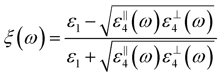
As the NPs are separated from the interface by a thin spacer layer, it is assumed that its relative permittivity is the same as that of the bulk ε1 = ε3. Keeping in mind the electrotunable photonic systems, the bulk will be the electrolytic solution, to which we typically assign the optical dielectric constant of water, 1.78. The image charge screening factor for the HMM reads (for derivation see the ESI†):
| | 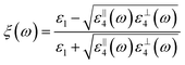 | (10) |
with
ε‖4(
ω)(
ε⊥4(
ω)) being the parallel (perpendicular) permittivity of the HMM, given by
eqn (1) and (2) when the HMM has the nanosheet geometry. When the fill fraction of the HMM is 0% metal, the material behaves as a pure dielectric returning the expected results and, similarly, when the fill fraction is set to 100% metal, the expected results for NPs above a metal film are observed. Due to the thickness of the HMM layer, as well as its metallic nature, it is assumed the image is not seen beyond the HMM. In all case studies here, for the HMM metal component, we will consider silver, as typically fabricated.
The NPs are assumed to form a hexagonal lattice. This is because, in experiments, NPs are functionalized by ligands with charged terminal groups, and thus they electrostatically repel each other. Consequently NPs, at least if they are spherically shaped, adopt this energetically optimal arrangement. There is always some degree of disorder which slightly shifts the NPs from their ideal positions. But as characteristic distances between the NPs in the array are much smaller than the wavelength of incident light, the differences in optical response that may have been caused by this mild disorder are negligible. More specifically, the positioning of the reflectance peaks and dips would remain practically in place, both in terms of wavelength and intensity.
Therefore the lattice dependent parameters for the effective polarizability of each NP, corresponding to this structure (eqn (11A)–(11D)) are defined as:36
| |  | (11A) |
| |  | (11B) |
| |  | (11C) |
| |  | (11D) |
here
a is the lattice constant and
h is the distance of the centre of the NP from the interface (
h =
R +
hs). When looking at the expression for the effective polarizability, there are multiple lattice dependent parameters which account for different interactions of the NPs with different parts of the system.
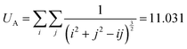
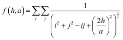
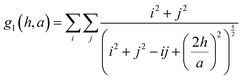
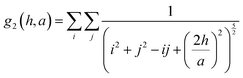
UA is the interaction of the NPs with each other in the 2D lattice, while the
f(
h,
a),
g1(
h,
a) and
g2(
h,
a) functions account for the interactions with the images of the surrounding NPs, as well as the interaction of each NP with its own image.
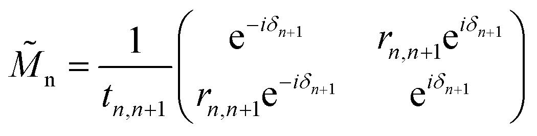
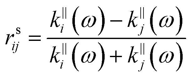
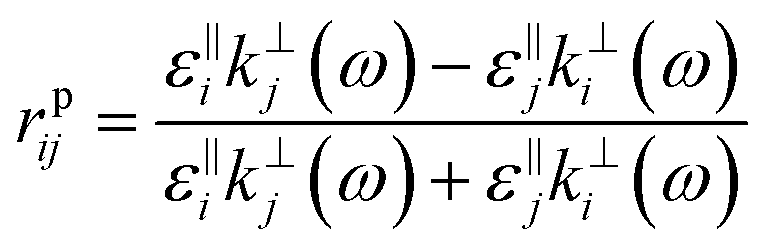
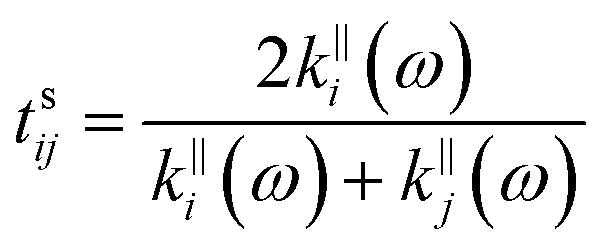
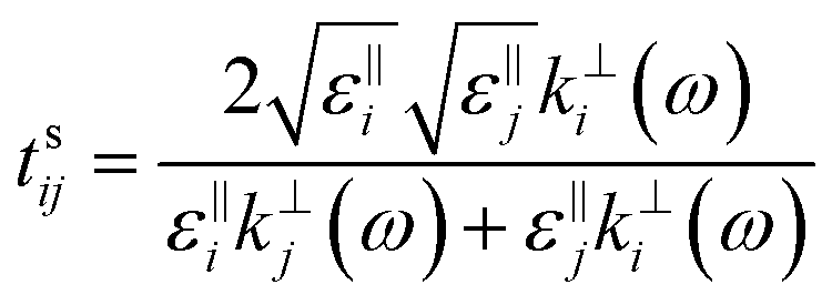
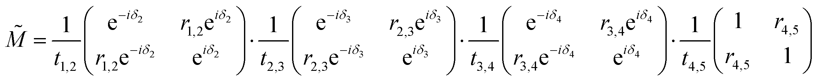
These results for the respective permittivity of the different layers allow the optical properties to be calculated when used in conjunction with the Fresnel equations. This is calculated by using the transfer matrix ![[M with combining tilde]](https://www.rsc.org/images/entities/i_char_004d_0303.gif) n, which determines how the interface between the n and n + 1 layers behaves. This is done in terms of the reflection (r) and transmission (t) coefficients for the interface, as given by the matrix:
n, which determines how the interface between the n and n + 1 layers behaves. This is done in terms of the reflection (r) and transmission (t) coefficients for the interface, as given by the matrix:
| | 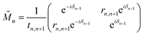 | (12) |
with
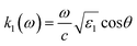
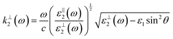
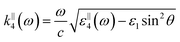
δn+1 being the phase shift determined by the wave vector and the thickness of the layer in question, here these are expressed as
δ‖2,⊥ =
k‖,⊥2d,
δ3 =
k3hs and
δ‖,⊥4 =
k‖,⊥4hf. The reflection and transmission coefficients at the interface between layers
i and
j are expressed as:
| | 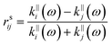 | (13A) |
| |  | (13B) |
| | 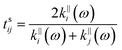 | (14A) |
| | 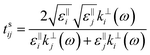 | (14B) |
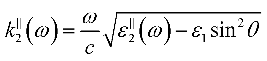
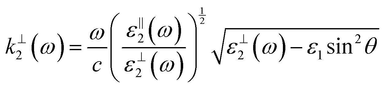
with the wave vectors defined here given by
| |  | (15A) |
| |  | (15B) |
| |  | (15C) |
| |  | (15D) |
| |  | (15E) |
| |  | (15F) |
| |  | (15G) |
The total transfer matrix is then extended for the 5-layer stack model, and it is the product of the individual transfer matrix at each interface.
=
1·
2·
3·
4 can be written as:
| |  | (16) |
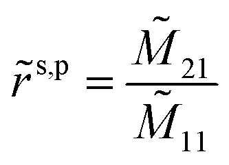
This gives the reflection coefficient as

and the transmission coefficient given by

where
11 and
21 are elements of the total transfer matrix. The reflection (
Rs,p), transmission (
Ts,p) and absorption (
As,p) are then determined by:
| | 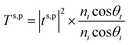 | (18) |
| | | As,p = 1 − Ts,p − Rs,p | (19) |
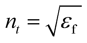
where

,

, where
εf and (
εi) are the permittivities of the final and initial) layers respectively.
θi is the angle of incidence and
is the angle of transmission.
Compared to the 4-layer stack model detailed in ref. 4, the model outlined here is of similar type, with the only difference that the current equations describe a 5-layer system (Fig. 2), where the 5th layer is considered semi-infinite.
Note that the generic Maxwell–Garnett approximation for the description of the optical dielectric response of a layered HMM is valid when the wavelength of light is larger than the thickness of individual sheets. We are considering the systems with sheet thickness of several nm, so the validity of this approximation is warranted. The dielectric functions of the metallic sheets in the HMM were considered depending only on the frequency of light (in Drude–Lorenz approximation) but not on wave-number, so the nonlocal electrodynamic effects37 are neglected. This is, however justified by the substantial, few nm thickness of the sheets. Indeed, in our present paper we look at the far field response, at wavelengths much greater than those structural characteristic lengths, and thus the effective medium approach, with no account of spatial dispersion, is expected to work well. This issue was investigated in a previous paper,38 in which the effect of layer spacing on the system's response to various Fourier components was analyzed.
In addition, it would be legitimate to ask why we did not take into account nonlocal effects in the NP array and can we expect deviations from the effective medium theory on that front? In ref. 39 it has been demonstrated that for the medium size of NPs, 20 nm in diameter or so (we consider even larger than that), nonlocal effects do matter only when NPs are just a few Angstrom apart. In the case that we consider the minimal distance between NPs is at least 2 nm, so we can neglect the effect of spatial dispersion of the dielectric constant of the metal and all the complexities of its implementation within the physical bounds of NP39 (for review see ref. 40). Such approximation has experimental approval. In our earlier theory5 and experiments2 on adsorbed NP arrays on purely metallic substrates, the wavelength of light was much greater than the size of NPs and inter-NP spacings, and that was good for the (i) applicability of the effective medium theory for the description of the optical response of NP arrays; and (ii) neglect of the spatial dispersion in the description of the optical response of individual NPs: the results of the theory were in excellent accordance with experimentally measured spectra.2,41
4. Results and discussion
4.1. Light reflection from Au NP arrays on HMMs
The precise wavelength where the HMM transitions from dielectric to metal-like behavior is directly correlated with the metal fraction, as shown in eqn (1) and (2). Consequently, the larger the metal fraction, the more blue-shifted is the transition wavelength. This can be seen in Fig. 3A, where the HMM varies from a completely transparent dielectric (TiO2), corresponding to a ff = 0, to the fully reflective (in the visible) silver, ff = 100%. In between these extremes, there lies a material which reflects more and more of the visible spectrum as the silver fraction increases.
 |
| | Fig. 3 Reflectance profile for a nanosheet HMM of different metal fractions. Panels: (A) without NPs and (B) with 20 nm-radius Au NPs. Curves correspond to different percentage fractions of Ag, the so-called filling fraction percentage (ff) of the metal in the multilayer HMM stack, as labelled on each curve. Calculations performed via the 5-layer stack model, ε1 = ε3 = 1.78, ε5 = 6.67, hs = 1 nm, hf = 200 nm, a = 3R (cf.Fig. 2). | |
It is worth noting that even in the region where the HMM behaves as a dielectric, its permittivity is not identical to the one of its constituents TiO2 dielectric. This difference, combined with the large 200 nm thickness of the material generates Fabry–Perot like oscillations, which can be spotted at low wavelengths.
Fig. 3B shows the effect of the addition of NPs on top of the HMM substrate, a system which exhibits the combination of the NP on window and NP on mirror effects described in ref. 1 and 2. In other words, NPs generally enhance the reflectance at low wavelengths, where the HMM exhibits dielectric-like behaviour. At the same time, part of the large wavelength spectrum is reduced by significant quenching effects, similar to the NP on mirror system. Depending on how the resonance wavelength of the NP plasmons is positioned compared to the wavelength at which HMM's optical response changes from the dielectric- to metal-like, the balance could tilt more towards enhancing reflectance in the dielectric region or quenching it in the metallic region.
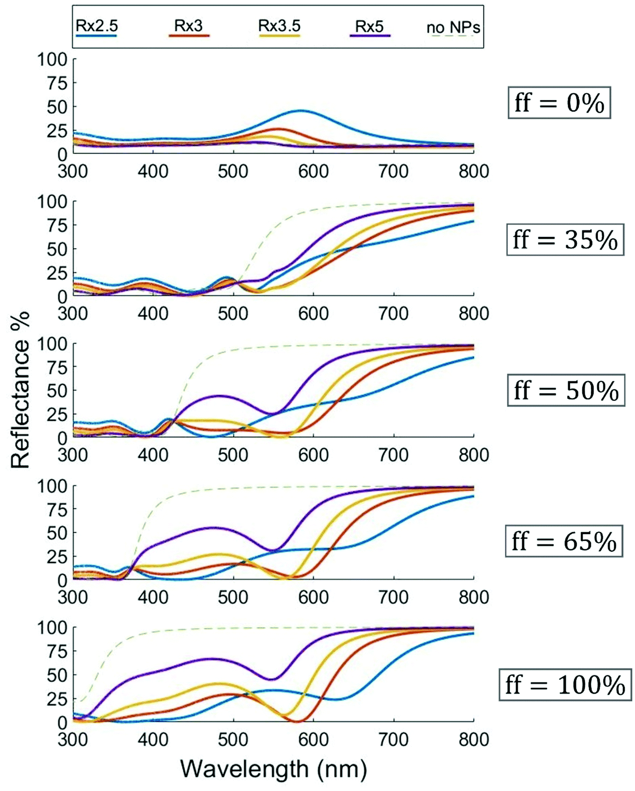
The change in the gaps between NPs can be used to shift the balance between the reflectance enhancement in the region where HMM's optical response is dielectric like and the reflectance quenching in the region of metallic-like response. Considering that reducing the NP gaps strengthens the coupling between the localized plasmons, one would expect this to affect both the reflectance enhancement and reflectance quenching (occuring simultaneously in their respective parts of the spectrum). The enhanced coupling affects the localized plasmons resonance frequency, particularly well seen in the 0% silver panel of Fig. 4, where there is negligible coupling between the localized plasmons and the plasmon modes in the substrate. The red shift of the reflectance peak with decreasing gap is a clear indication of the decrease of the localised plasmon resonance frequency. Therefore, the closeness of this frequency to the ‘HMM transition wavelength’ results in roughly equal balance between the reflectance enhancement and quenching. A particularly interesting combination of these effects can be seen in Fig. 4 – 50% silver panel, where the closeness of the plasmon frequency to the HMM transition point generates a wide (400–600 nm) weak reflectance region for a NP gap of 3R and even for 3.5 R (red and yellow curves, respectively).
 |
| | Fig. 4 Reflectance profiles for nanosheet HMMs of different metal fractions with different inter-NP spacings. Color coding as indicated in the top-box-legend corresponds to different center-to-center inter-NP distances (measured in NP-radius) in the hexagonal array of NPs. Each panel corresponds to displayed Ag fractions (ff) in the multilayer stack Ag/TiO2 HMM. Curves are calculated via the 5-layer stack model for R = 20 nm, hs = 1 nm, hf = 200 nm, ε1 = ε3 = 1.78, ε5 = 6.67. | |
Compared to the purely metallic substrate, where we also observed an absorption dip, the HMM case broadens the wavelength range where this absorption occurs. In particular, the 50% metallic HMM in Fig. 4 displays the widest absorption range. To unravel the nature of this effect, we also performed COMSOL simulation of the electric field distribution in this system for two frequencies, corresponding to maximal absorption and high reflectance, respectively, see Fig. 5. The details how this figure was generated, as well as its broader discussion can be found in the ESI.†
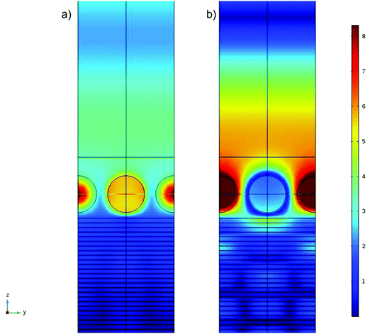 |
| | Fig. 5 The magnitude of electric field of light, computed within the COMSOL simulation cell of the NP array on HMM layered system with 50% of metallic sheets. The thickness of each metallic (silver) and dielectric (TiO2) sheet is 5 nm; NPs are 40 nm in diameter, surface-to-surface separated by one radius. All other parameters are as in Fig. 4 (the displayed plots correspond to the brown curve, of its middle row, ff = 50%). Panels show the electric field magnitude corresponding to the light of wavelength of (a) 530 nm and (b) 750 nm, which correspond, to high absorption and to high reflectance situations, respectively. Both panels show the maps along the YZ-plane, with the incident light linearly polarized in X-direction (perpendicular to the figure plain). The magnitude of the field is defined by the color bar on the right side, given in arbitrary units. In both panels the YZ plane runs across the central NP, and the hot spots that we see there are located between NPs in the simulation cell. Panel (a) shows concentration of electric field in those hot spots with no penetration of the field into HMM and very little field radiated back from the interface. This indicates high absorption of light of 530 nm wavelength by this system. Panel (b) shows almost the opposite: some penetration into the HMM and substantial radiation back from the interface, which is a signature of high reflection of the light of 750 nm wavelength. | |
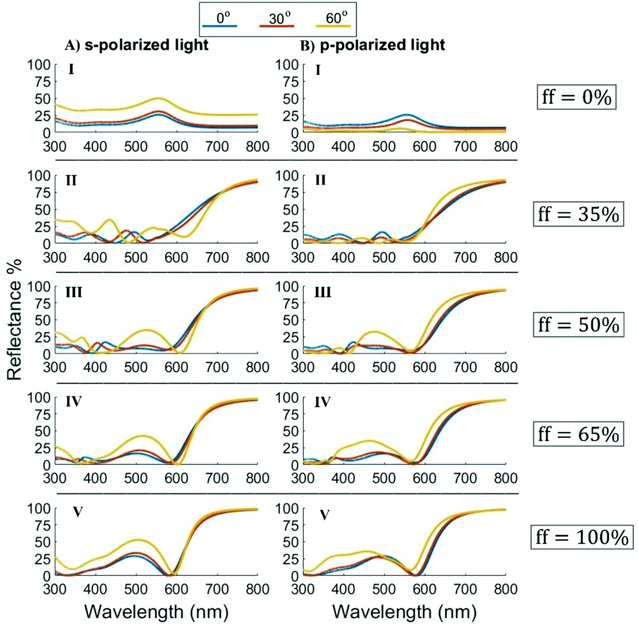
The incidence-angle-dependence depicted in Fig. 6, panels A.I and B.I is comparable to a reflectance profile observed at the interface between two dielectrics. More specifically, the s-polarization component increases continuously with the incidence angle, the p-components at both 30° and 60° are lower than reflection at normal incidence. This is due to the typical behavior of the reflectance of p-polarized light, which slowly decreases with angle all the way down to the Brewster angle, where it reaches zero, then increasing again up to total reflectance close to 90°.
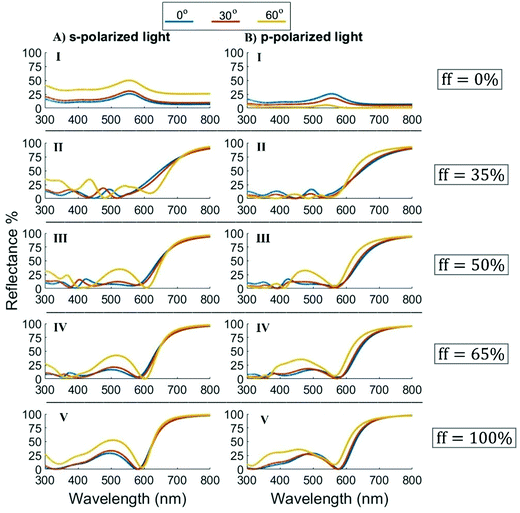 |
| | Fig. 6 Reflectance profile for a nanosheet HMM of different metal fractions with different angles of incidence. Color coding of curves correspond to indicated angles of incidence in the top box of the figure. Curves calculated for a hexagonal NP array above a Ag/TiO2 multilayer HMM stack, with all other parameters as in Fig. 4, for the Ag fill fraction as indicated in each panel. | |
The general trend is for the s polarization to increase and the p polarization to decrease with angle of incidence, a pattern which also holds for the metallic range of the HMM. However, as the incidence angle approaches the Brewster angle, the p-reflectance in the metallic region will only decrease slightly (compared to the s-reflectance), while the low wavelength region pushes the 60° p-reflectance to very small values. This can be observed most easily for the HMM substrates in Fig. 6A.II and B.II, where the discrepancy between s and p polarizations is greatest at short wavelengths (dielectric region) and relatively small at long wavelengths (metallic region). As the metal fraction in the HMM increases, the dielectric region shrinks and thus, the qualitative difference between the s and p reflectance profiles diminishes significantly.
4.2. Fabry–Perot interferometer based on an NP array on HMM plate
Another interesting instrument, well used in optics, is the Fabry–Perot interferometer,42,43 the model describing this is reproduced in the ESI† and is an extension to that presented in ref. 44, in which the cavity walls were purely metallic. The present study focuses on a similar device, but in which one of the cavity walls is replaced by HMM. The wide usage of this device stems from the very sharp transmission peaks that it can generate in the visible range.
It is worth mentioning that the combination of Fabry–Perot cells, HMMs and NP arrays is being analyzed here for the first time. We find a counter-intuitive change in transmittance peaks, as explained below. The interference-based selectors, such as the Fabry–Perot ones, are generally incredibly sensitive devices, emphasizing yet again the importance of their study. They can detect even the slightest changes in parameters, caused, for example, by temperature differences, pressure changes, and even by acoustic waves.45 The one considered here allows for fine tuning of the light transmission via the voltage-controlled variation of NP-array density, like it has been suggested in ref. 44, but with different characteristics provided by the usage of HMM- components of different metal-dielectric fractions.
Fig. 8B shows transmittance for a typical configuration of such a device, where the interferometer has a 30 nm thick silver layer on top and another 50 nm silver layer at the bottom. In this instance, the visible range peaks go up to 40–50% transmission. A Fabry–Perot cell with thin semi-transparent silver film electrodes on glass and silver NPs electrosorbed on them have been described in ref. 44. It was natural to extend the present study to a similar Fabry–Perot device, but in which a bottom layer (see Fig. 7) is made of nanosheet HMM and potentially covered by NPs (see definition of the “top” and “bottom” in the figure caption). Fig. 8B shows the transmittance profile of the new, HMM-based (50% silver) interferometer, where a few distinct characteristics are observed. The configuration in Fig. 8 is particularly interesting to study because the HMM was taken to be 100 nm thick, so both the pure silver and HMM systems have the same amount of silver in the bottom layer, as well as in the top one.
 |
| | Fig. 7 The sketch of cross-section of the NP-based Fabry–Perot interferometer (a) and its mapping (b) on the effective medium model (cf.Fig. 2). In both pictures light shines from the left side, so it will be sometimes referred in the text as the ‘top’ side, whereas the right side (where the HMM is represented in brown) will be referred to as the ‘bottom’ side. hs, hf and h have the same significance as in Fig. 2, with the key difference that the top layer has a thin silver film instead of HMM. Additionally, the parameter L denotes the length of the Fabry–Perot cavity. | |
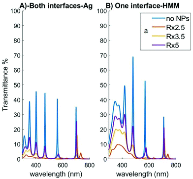 |
| | Fig. 8 Transmission of light through a Fabry–Perot interferometer based on an array of NPs above Ag/TiO2 HMM slab. (A) Pure Ag sheets at both sides of the device, of thickness hf = 30 nm (top plate) and hf = 50 nm (bottom plate) respectively, with light incident from the top. (B) Bottom plate replaced with HMM of thickness hf = 100 nm and Ag fraction ff = 50%. In both cases NPs are assembled on the bottom plate, where the labelled curves correspond to indicated NP center-to-center distances in the hexagonal array. The other parameters used in the 5-layer stack model calculations are: R = 20 nm, hs = 1 nm, ε1 = ε9 = 6.67, ε3 = ε5 = ε7 = 1.78. The corresponding curves for reflection and absorption are given in ESI,† Fig. S7. | |
On the one hand, the HMM transition wavelength for 50% silver is around 450 nm, meaning the transmission peaks at 350 and 400 nm that occur for a pure silver layer at the bottom are located in the dielectric region of the HMM. As a result, those two peaks are no longer well distinguished due to the inability of the HMM to reflect a significant amount of light back into the cavity in that frequency range, thus reducing the number of sharp peaks available.
Note that the peak at 470 nm is located in the metallic region of the HMM, meaning it is still present in the HMM interferometer, as seen in Fig. 8B. However, its near vicinity to the HMM transition wavelength weakens the metallic character of the HMM at 470 nm. As a result, the intensity of this transmission peak increases substantially (up to 70%), while keeping practically the same sharpness. This phenomenon emphasizes that HMM could, at least in principle, be chosen to enhance one particular transmission peak of the FP interferometer, while maintaining its sharpness and the possibility of quenching it by assembling a NP array on top of the bottom layer.
All in all, in Fig. 8 we see a peak in transmission at wavelength of 470 nm, which is higher than it would have been for a homogeneous silver sheet instead of HMM, but in the vicinity of the peak the HMM changes its mode of performance from Type I to Type II.
A metamaterial exhibiting the reverse transition (from Type II to Type I), such as a nanowire HMM, could, in principle, exhibit this effect as well. As long as one of the transmission peaks lies in the vicinity of the HMM transition wavelength, one would expect a similar effect to occur. However, quantitative predictions can only be made with proper modelling of this HMM, a model that needs to estimate the transition wavelength, as well as the positions of all the transmission peaks in the Fabry–Perot device.
5. Conclusion
The use of hyperbolic metamaterials as a substrate for self-assembled NP arrays has proven to be an almost ideal way to combine the optical effects seen in the NP on metal and NP on dielectric systems. Furthermore, the relative balance of the two limiting effects was shown to depend on the wavelength of localized plasma excitations in the array of NPs (and due to the coupling of those modes in the array, those depend on the array density), and how it relates to the wavelength at which the HMM response transits from Type I to Type II.
Finally, the use of the HMM in the bottom layer of a Fabry–Perot interferometer has shown the potential to enhance one transmission peak at the expense of two others when compared to a pure silver bottom layer inside the same system.
With a perspective or manipulation of NP densities in electrochemical cell demonstrated in ref. 1, 2 and 41, these findings open new opportunities in electrochemical photonics.
Conflicts of interest
There are no conflicts to declare.
Acknowledgements
We are indebted to our co-authors on previous publications – Joshua Edel, Ye Ma, and especially Debabrata Sikdar, for many useful discussions that have influenced this new work. We thank Engineering and Physical Sciences Research Council (Funder ID: 10.13039/501100000266) for financial support through the grants EP/L015579/1, P90419 EPSRC IAA, and EP/L02098X/1.
References
- Y. Montelongo, D. Sikdar, Y. Ma, A. J. S. McIntosh, L. Velleman, A. R. Kucernak, J. B. Edel and A. A. Kornyshev, Nat. Mater., 2017, 16, 1127–1135 CrossRef CAS PubMed.
- Y. Ma, C. Zagar, D. J. Klemme, D. Sikdar, L. Velleman, Y. Montelongo, S. H. Oh, A. R. Kucernak, J. B. Edel and A. A. Kornyshev, ACS Photonics, 2018, 5, 4604–4616 CrossRef CAS.
- J. B. Edel, A. A. Kornyshev, A. R. Kucernak and M. Urbakh, Chem. Soc. Rev., 2016, 45, 1581–1596 RSC.
- D. Sikdar and A. A. Kornyshev, Sci. Rep., 2016, 6, 1–16 CrossRef PubMed.
- D. Sikdar, S. B. Hasan, M. Urbakh, J. B. Edel and A. A. Kornyshev, Phys. Chem. Chem. Phys., 2016, 18, 20486–20498 RSC.
- A. A. Kornyshev, J. Solid State Electrochem., 2020, 24, 2101–2111 CrossRef.
- M. E. Flatté, A. A. Kornyshev and M. Urbakh, J. Phys. Chem. C, 2010, 114, 1735–1747 CrossRef.
- P. K. Jain and M. A. El-Sayed, Chem. Phys. Lett., 2010, 487, 153–164 CrossRef CAS.
- S. K. Ghosh and T. Pal, Chem. Rev., 2007, 107, 4797–4862 CrossRef CAS.
- J. J. Mock, R. T. Hill, A. Degiron, S. Zauscher, A. Chilkoti and D. R. Smith, Nano Lett., 2008, 8, 2245–2252 CrossRef CAS.
- Y. Guo, W. Newman, C. Cortes, Z. Jacob, C. L. Cortes, S. Molesky, Z. Jacob and E. Narimanov, Opt. Express, 2013, 21, 7614–7632 CrossRef.
- A. Pianelli, A. Pianelli, R. Kowerdziej, R. Kowerdziej, M. Dudek, K. Sielezin, M. Olifierczuk and J. Parka, Opt. Express, 2020, 28, 6708–6718 CrossRef.
- P. Shekhar, J. Atkinson and Z. Jacob, Nano Convergence, 2014, 1, 1–17 CrossRef PubMed.
-
I. I. Smolyaninov, Hyperbolic Metamaterials, Morgan and Claypool Publishers, Bristol, 2018 Search PubMed.
- C. Guclu, S. Campione and F. Capolino, Phys. Rev. B: Condens. Matter Mater. Phys., 2012, 86, 205130 CrossRef.
- A. Andryieuski, S. v Zhukovsky, A. v Lavrinenko, J. K. Kitur, E. E. Narimanov, M. A. Noginov, E. Narimanov, H. Li, Y. A. Barnakov and T. U. Tumkur, Opt. Express, 2014, 22, 14975–14980 CrossRef PubMed.
- E. E. Narimanov, H. Li, Yu. A. Barnakov, T. U. Tumkur and M. A. Noginov, Opt. Express, 2013, 21, 14956 CrossRef CAS PubMed.
- C. Guclu, S. Campione and F. Capolino, Phys. Rev. B: Condens. Matter Mater. Phys., 2014, 89, 155128 CrossRef.
- J. Zhou, A. F. Kaplan, L. Chen and L. J. Guo, ACS Photonics, 2014, 1, 618–624 CrossRef CAS.
- W. Yan, M. Wubs and N. A. Mortensen, Phys. Rev. B: Condens. Matter Mater. Phys., 2012, 86, 205429 CrossRef.
- J. Yin, X. Zhao and Z. Su, Opt. Express, 2015, 23, 1679–1690 CrossRef PubMed.
- L. Yu Beliaev, O. Takayama, P. N. Melentiev, A. V. Lavrinenko, L. Yu.
Beliaev, O. Takayama, P. N. Melentiev and A. V. Lavrinenko, Opto-Electronic Adv., 2021, 4, 210031 CAS.
-
X. Luo, Handbook of Laser Micro- and Nano-Engineering, 2020, 1–40 Search PubMed.
- X. Luo, M. Pu, Y. Guo, X. Li and X. Ma, Adv. Photonics Res., 2021, 2, 2100023 CrossRef.
- M. A. Baqir, P. K. Choudhury and Q. A. Naqvi, Optik, 2021, 246, 167850 CrossRef CAS.
- C. H. Lai, G. A. Wang, T. K. Ling, T. J. Wang, P. K. Chiu, Y. F. Chou Chau, C. C. Huang and H. P. Chiang, Sci. Rep., 2017, 7, 1–8 CrossRef.
-
R. M. K. Czajkowski, M. Bancerek, T. J. Antosiewicz and R. Kotyński, Proceedings of Metamaterials XII, SPIE-Optics+ Optoelectronics, 2019, vol. 110250D, pp. 21–28.
- A. Poddubny, I. Iorsh, P. Belov and Y. Kivshar, Nature Photonics, 2013, 7, 948–957 CrossRef CAS.
- H. N. S. Krishnamoorthy, Z. Jacob, E. Narimanov, I. Kretzschmar and V. M. Menon, Science, 2012, 336, 205–209 CrossRef CAS PubMed.
- L. Ferrari, C. Wu, D. Lepage, X. Zhang and Z. Liu, Prog. Quantum Electron., 2015, 40, 1–40 CrossRef.
- F. Yang, K. Ding and J. B. Pendry, Nanophotonics, 2020, 10, 545–548 Search PubMed.
- Y. L. Zhang, J. B. Pendry and D. Y. Lei, Phys. Rev. B, 2017, 96, 035430 CrossRef.
- J. B. Pendry, D. Schurig and D. R. Smith, Science, 2006, 312, 1780–1782 CrossRef CAS PubMed.
- J. B. Pendry, A. Aubry, D. R. Smith and S. A. Maier, Science, 2012, 337, 549–552 CrossRef CAS PubMed.
-
K. V. Sreekanth, M. ElKabbash, V. Caligiuri, R. Singh, A. de Luca and G. Strangi, New directions in thin film nanophotonics, Progress in Optical Science and Photonics, Springer-Nature, Singapore, 2019, vol. 6 Search PubMed.
- B. N. J. Persson and A. Liebsch, Phys. Rev. B: Condens. Matter Mater. Phys., 1983, 28, 4247 CrossRef CAS.
- Y. Luo, A. I. Fernandez-Dominguez, A. Wiener, S. A. Maier and J. B. Pendry, Phys. Rev. Lett., 2013, 111, 093901 CrossRef PubMed.
- B. Wood, J. B. Pendry and D. P. Tsai, Phys. Rev. B: Condens. Matter Mater. Phys., 2006, 74, 115116 CrossRef.
- F. J. G. de Abajo, J. Phys. Chem. C, 2008, 112, 17983–17987 CrossRef.
- N. J. Halas, S. Lal, W. S. Chang, S. Link and P. Nordlander, Chem. Rev., 2011, 111, 3913–3961 CrossRef CAS PubMed.
- Y. Ma, D. Sikdar, A. Fedosyuk, L. Velleman, D. J. Klemme, S. H. Oh, A. R. J. Kucernak, A. A. Kornyshev and J. B. Edel, ACS Nano, 2020, 14, 328–336 CrossRef CAS PubMed.
- M. Rajibul Islam, M. Mahmood Ali, M. H. Lai, K. S. Lim and H. Ahmad, Sensors, 2014, 14, 7451–7488 CrossRef PubMed.
-
F. L. Pedrotti, L. M. Pedrotti and L. S. Pedrotti, Introduction to Optics, Cambridge University Press, 2017 Search PubMed.
- D. Sikdar and A. A. Kornyshev, Nanophotonics, 2019, 8, 2279–2290 CAS.
- M. Rajibul Islam, M. Mahmood Ali, M. H. Lai, K. S. Lim and H. Ahmad, Sensors, 2014, 14, 7451–7488 CrossRef PubMed.
|
| This journal is © The Royal Society of Chemistry 2022 |
Click here to see how this site uses Cookies. View our privacy policy here. 
 Open Access Article
 This Open Access Article is licensed under a Creative Commons Attribution-Non Commercial 3.0 Unported Licence
 b,
John B.
Pendry
a and
Alexei A.
Kornyshev
b,
John B.
Pendry
a and
Alexei A.
Kornyshev


 and the transmission coefficient given by
 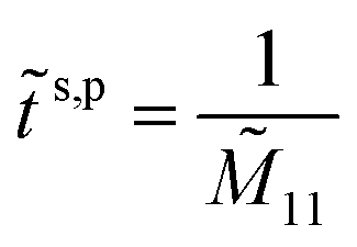 where
where 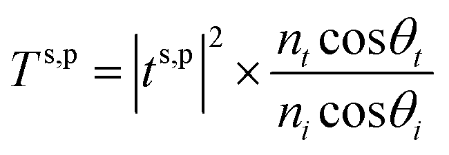
 ,
,  , where εf and (εi) are the permittivities of the final and initial) layers respectively. θi is the angle of incidence and
  is the angle of transmission.