
Extended linear detection range of a Bi0.5Na0.5TiO3 thin film-based self-powered UV photodetector via current and voltage dual indicators†
Mingyue
Tian
ab,
Lan
Xu
a,
Huiyu
Dan
ab and
Ya
Yang
 *abc
*abc
aCAS Center for Excellence in Nanoscience, Beijing Key Laboratory of Micro-nano Energy and Sensor, Beijing Institute of Nanoenergy and Nanosystems, Chinese Academy of Sciences, Beijing 101400, P. R. China. E-mail: yayang@binn.cas.cn
bCenter on Nanoenergy Research, School of Physical Science and Technology, Guangxi University, Nanning 530004, P. R. China
cSchool of Nanoscience and Technology, University of Chinese Academy of Sciences, Beijing 100049, P. R. China
First published on 1st August 2022
Abstract
Ferroelectric materials are widely recognized for their ability to generate photovoltaic voltages larger than their bandgap, making them ideal candidates for photodetector applications. Here, we report a self-powered UV photodetector based on a Bi0.5Na0.5TiO3 (BNT) thin film prepared by the sol–gel method. Compared with conventional photodetectors based on a single detection indicator, the demonstrated photodetector realizes UV light intensity detection over a wide linear range using a current and voltage dual indicator detection method. When the UV light intensity is lower than 1.8 mW cm−2, the voltage can be used to detect the light signal. Conversely, the current can be utilized to detect the signal. This method not only broadens the linear detection range of UV light intensity, making it possible to detect weak UV light of 45.2 nW cm−2, but also allows the detector to maintain relatively high sensitivity within the detectable range. To investigate the distribution of spatial UV light intensity, a self-powered photodetector array system has been utilized to record the output voltage signals as a map.
New conceptsMost conventional ferroelectric thin film based UV photodetectors use a single detection indicator (current) to detect UV light signals, which can only detect UV light at the μW/cm2 level, and lack ultra-sensitive detection of UV light at low power levels. However, the reported sodium bismuth titanate ferroelectric film-based UV photodetector can broaden the linear detection range of 365 nm UV light by combining current and voltage dual detection indicators, where the voltage was utilized to detect signals at low light intensity and the current was utilized to detect signals at high light intensity. This detection mode not only enables ultrasensitive detection of ultra-low UV light intensity, but also enables linear detection over the entire detection range. The reported work will provide new ideas and thoughts for the next generation of nano-energy materials for photodetectors. |
1. Introduction
Ultraviolet (UV) light has become more widely employed as science and technology have progressed. However, UV light cannot be observed by the naked eye, and since people need to monitor and quantify it, UV-detection technologies have advanced quickly. UV-detection technology has numerous applications in both military and civilian settings, including missile warning and tracking, astronomy, disaster, weather forecasts, maritime oil pollution monitoring, and biomedicine.1–9 UV photodetectors can be classified into three main development stages, namely, UV photomultiplier tubes, Si-based UV photodetectors, and third-generation broadband semiconductor materials (such as ZnO-based, GaN-based, and SiC and Ga2O3-based).10–16 Although UV photomultiplier tubes have a stable and quick response, allowing for high-response UV detection, the photomultiplier tube requires a large power source and cathode cooling. This makes it bulky and power-hungry as well as unsuitable for practical applications. Si-based UV photodetectors do not have a high response to the total UV band as they have a small forbidden band width.17,18 As a result, they have a relatively low rejection of visible light and are not highly reliable. Thanks to their large band width, wide-band semiconductor UV photodetectors are sensitive to UV light only and do not respond to infrared and visible light. Therefore, they do not require filters and have natural band selectivity, allowing them to achieve a small size, simple structure, low noise, and high-quality response. Although some breakthroughs have been made in the research on wide-band semiconductors,19,20 their high cost due to the quality issues of the required materials and the complexity of the device-fabrication process (e.g., surface modification and material surface functionalization)21,22 have made it that wide-band semiconductor UV detectors are not yet ready for commercial applications. As a result, developing self-powered UV photodetectors with outstanding UV detection capability at a cheap cost and with a simple manufacturing technique is critical.Recent research has revealed that ferroelectric materials have promising applications in new solar cells, photodetectors and photovoltaic memory devices.23–26 This can be mainly explained by their bandgap-independent open-circuit voltage and the generation mechanism of photogenerated carriers. In ferroelectric-based self-powered photodetectors, there are two main mechanisms driving the separation of photogenerated electron–hole pairs: the depolarization field and Schottky barrier formed between the ferroelectric material and the metal electrode.27 Recently, Chen et al. designed a self-powered photodetector based on the depolarization field (Edp) and built-in electric field at the p–n junction (Ep–n), and this showed enhanced device performance through the coupling effect between Ep–n and Edp.28 Yang et al. created a novel photodetector based on a lead zirconate titanate (PZT) material using the electrostatic spinning method as well as the sol–gel approach.29 Although self-powered UV light detection was realized by using the photo-induced pyroelectric effect in PZT, it is undeniable that PZT contains a large amount of harmful substances, such as lead. So, it will inevitably cause a series of problems against environmentally friendly development in the processes of preparation, usage, and disposal. Therefore some ferroelectric materials that are both environmentally friendly and harmless to human beings are attracting more and more attention. In comparison to bulk materials, such as ceramics, thin films have a faster response time, higher photoelectric conversion efficiency, and are easier to apply in integrated circuits and systems. Among the lead-free piezoelectric ceramic systems, sodium bismuth titanate (Bi0.5Na0.5TiO3, BNT) ceramic has received widespread attention because of its high Curie temperature, good electromechanical coupling coefficient, and outstanding ferroelectric and piezoelectric properties. However, the majority of researchers have devoted themselves to its applications in ferroelectric, dielectric, piezoelectric, energy storage, and doping modifications, while neglecting its photovoltaic properties.30,31 Here, a BNT-based self-powered UV photodetector was prepared by the sol–gel method, and some essential photovoltaic properties of the ITO/BNT/LNO/glass as a self-powered UV photodetector were investigated by electrical tests and calculations. It was revealed that the device can broaden the linear detection range of 365 nm UV light by the dual-indicators detection of current and voltage. A feeble 365 nm UV light of 45.2 nW cm−2 could be detected, which is substantially lower than the lowest light intensity observed by prior ferroelectric photodetectors. This work thus demonstrated the future potential of BNT films as self-powered UV detectors, which is crucial for expanding the utilization of ferroelectric materials in self-powered UV detectors.
2. Results and discussion
2.1 Detection mechanism and characteristics of the ITO/BNT/LNO/glass UV photodetector
Fig. 1a shows a 3D microstructure simulation of the ITO/BNT/LNO/glass UV photodetector under 365 nm UV light. An energy band image and an electron transport mechanism diagram related to the BNT film were plotted in order to diagnose the generation and transport of photogenerated carriers, and to further explain the generation mechanism of photovoltaic current as well as photovoltaic voltage (Fig. S1, ESI†). The work functions of ITO and LNO were 4.8 and 4.5 eV,32,33 respectively. It was considered that the work function of the BNT thin film is smaller than both of them, as shown in Fig. S1c (ESI†). The ideal energy band diagram of the device was given without considering the BNT polarization state, as shown in Fig. S1a (ESI†). When a BNT film's spontaneous polarization is taken into account, the energy band image of the device was different, as shown in Fig. S1b (ESI†). The energy band diagram when spontaneous polarization was considered could be obtained from Fig. S1d (ESI†), since current flow from the LNO to the ITO was noticed during the I–t curve measurement. The energy level of the BNT changed up (down) when positive (negative) surface charge accumulated at the head (tail) of the polarization vector, resulting in a lower (higher) potential barrier; in other words, ϕ1' < ϕ1, ϕ2' > ϕ2. Under 365 nm UV light, the photogenerated electrons flowed to the ITO electrode and the photogenerated holes flowed to the LNO electrode, contributing to current generation in an external circuit. Fig. 1b presents a schematic diagram of the variation of the output voltage with light intensity. When voltage was chosen as the detection indicator, the sensitivity of the photodetector at light intensities less than 1.8 mW cm−2 (365 nm UV light) was better than that at other light intensities (obtained from the slope of the curve). On the contrary, when current was chosen as the detection indicator, the photodetector's sensitivity at light intensities over 1.8 mW cm−2 was better than that at other light intensities (Fig. 1c). This indicates that photovoltaic current and voltage can be combined for detection. When the light intensity was less than 1.8 mW cm−2, voltage was used to detect the 365 nm UV light signal. When the light intensity was more than 1.8 mW cm−2, the current was used to investigate the 365 nm UV light signal. By this method, the linear detection range of the ITO/BNT/LNO/glass UV photodetector was enlarged and the sensitivity of the photodetector was improved, with respect to using a single detection indicator (current or voltage), as shown in Fig. 1d.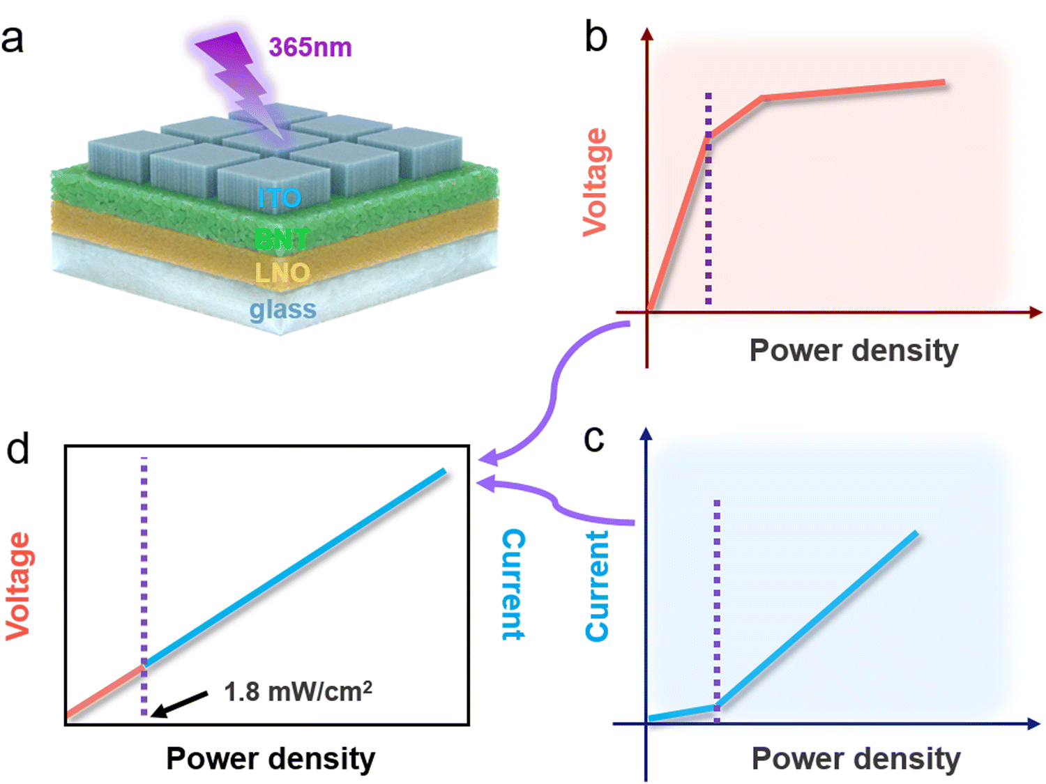 | ||
| Fig. 1 A schematic illustration of the device structure and the detection characteristics used for the detector. (a) Microstructure simulation of the ITO/BNT/LNO/glass UV photodetector under 365 nm light. (b) Schematic diagram of the photovoltaic voltage with light intensity. (c) Schematic diagram of the photovoltaic current with light intensity. (d) Schematic diagram of the photovoltaic voltage and short-circuit current with light intensity. | ||
2.2 Characterization and essential properties of the device
A photograph of the 15 mm × 15 mm ITO/BNT/LNO/glass device is shown in Fig. 2a. An XRD image of the BNT film can be seen in Fig. S2a (ESI†). The well-defined diffraction peaks could be nicely indexed to BNT's perovskite phase (JCPDS No. 36-0340), while the secondary phase peak of Na0.5Bi4.5Ti4O15 (hollow circle label) could be found at 2θ–30.7° (JCPDS No. 74-1318). Fig. 2b shows a scanning electron microscopy (SEM) picture of the device, where the thicknesses of ITO, BNT, and LNO were 244.6, 309.4, and 219.4 nm, respectively. SEM characterization of the BNT's surface is shown in Fig. S2b (ESI†). The volatilization of Bi3+ and Na+ could explain the small holes on the surface of the BNT film. In Fig. 2c and Fig. S2c (ESI†), the 2D and 3D atomic force microscopy (AFM) morphologies of the BNT films are shown, respectively. Fig. S2e (ESI†) shows a cross-sectional height trace of the BNT films, which corresponds to the white line on the topographic image (Fig. S2d, ESI†). From these figures, it can be seen that a good quality and uniform BNT film was prepared. In addition, we also measured the P–E loop of the Bi0.5Na0.5TiO3 thin film to verify its ferroelectric property (Fig. S3, ESI†).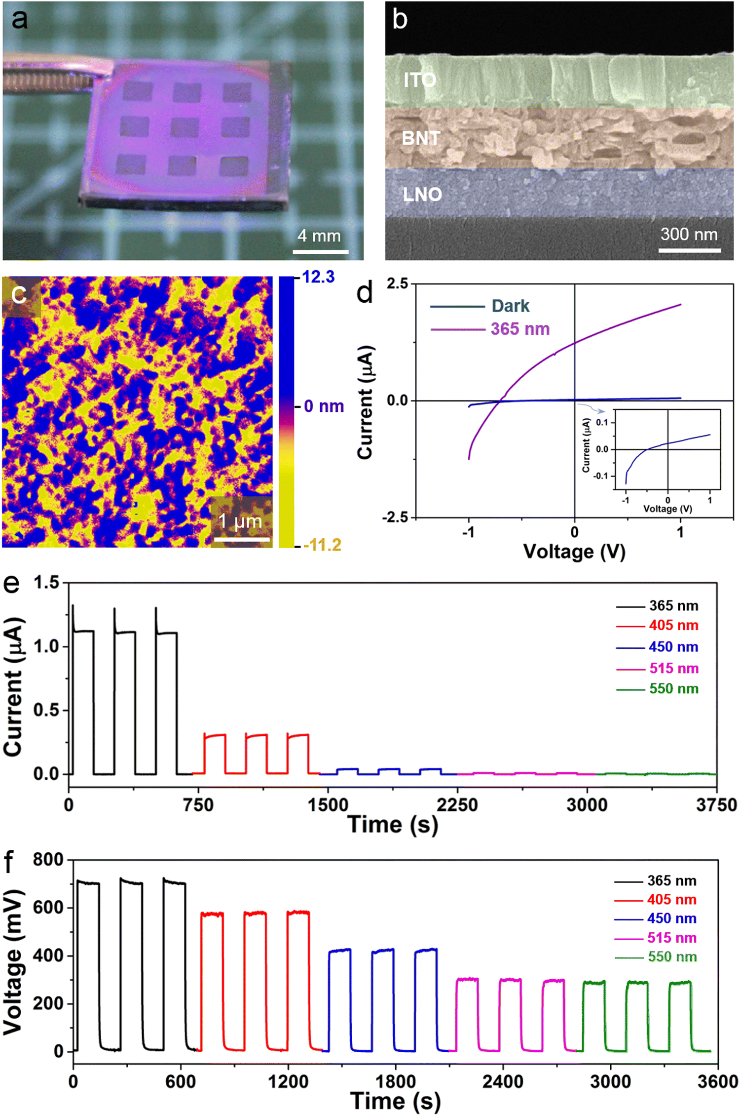 | ||
| Fig. 2 Characterization of the device and performance testing at different wavelengths. (a) Photograph of a 15 mm × 15 mm ITO/BNT/LNO/glass self-powered UV detector device. (b) Cross-sectional scanning electron microscopy image of the ITO/BNT/LNO/glass device. (c) AFM morphology image of a BNT film at the 5 μm scale. (d) I–V curves of the device in the dark state and under 365 nm UV light; the inset is the I–V curve in the dark state. (e) I–t curves for various wavelengths of light at the same light intensity. (f) V–t curves for various wavelengths of light at the same light intensity. | ||
The I–V characteristic curves of the ITO/BNT/LNO/glass device were tested in darkness and under 365 nm UV light irradiation (Fig. 2d), and the device exhibited a favorable UV response. The nonlinear I–V characteristic curve could identify the Schottky contact between the ITO electrode and the BNT thin film. Furthermore, Fig. S4 (ESI†) also summarizes the I–V curves under 365 nm UV irradiation with various light intensities. As the light intensity was increased from 10.63 nW cm−2 to 85.20 mW cm−2, the photovoltaic current also gradually increased. This was because that the increase in light intensity produced more electron–hole pairs that were subsequently separated by the internal field generated by the Schottky barrier, leading to a larger current.32 Meanwhile, to demonstrate that the photovoltaic current came from the BNT film rather than the LNO bottom electrode, a comparison experiment was also performed. As seen in Fig. S5a (ESI†), the current signal was obtained by spin-coating only the BNT film on the FTO glass, and Fig. S5b (ESI†) shows the current signal obtained by spin-coating only the LNO on the FTO glass. This could obviously prove that the photovoltaic current originated from the BNT film and not from the LNO film. Further, the I–t and V–t curves were measured at different wavelengths for the same light intensity (Fig. 2e and f), which obviously demonstrated that the device generated the strongest current and voltage signal under 365 nm UV light. The transmission and absorption spectra at different wavelengths in Fig. S6 (ESI†) further confirmed that the device had the optimal response to the 365 nm UV light. The output performance of the device under 365 nm UV light was also studied. The output current was tested at various load resistances to calculate the device's maximum output power. The following equation was used to calculate the output power:
| P = I2R |
2.3 Performance of the devices under 365 nm UV irradiation with different light intensities
Next, the device's photovoltaic performance was tested under various 365 nm UV light intensities. In order to further evaluate the device's photosensitive features, the light-intensity dependency of the output voltage and short-circuit current were measured independently under 365 nm UV light, as shown in Fig. 3. As the light intensity decreased from 8.52 × 10⁴ μW cm−2 to 1.06 × 10⁻² μW cm−2, both the voltage and current of the device progressively decreased. As is easy to see in Fig. 3a, the variation of current with light intensity was noticeable in the high light-intensity range (8.52 × 10⁴ μW cm−2 to 1.76 × 10³ μW cm−2), yet the current value was zero when the light intensity was less than 1.20 × 10² μW cm−2. Conversely, the voltage variation with light intensity became not so significant in the high light intensity range and more significant in a faint light intensity region (<1.76 × 10³ μW cm−2). Also, even when the light intensity was reduced to 4.52 × 10⁻² μW cm−2, the device still had a voltage response of 1 mV, as shown in Fig. 3b. In order to see more intuitively the change law of the current and voltage with light intensity, curves of the current and voltage with light intensity were plotted, as shown in Fig. S8 (ESI†). It was found that as the light intensity increased, the open-circuit voltage showed a law of change that first increased and then tended to remain constant, while the short-circuit current was practically directly proportional to the light intensity. Moreover, in the low light-intensity range, the variation of voltage with light intensity was more pronounced compared to the current. In the high light-intensity range, the variation of the current with the light intensity was more pronounced than that of the voltage. To further verify, the curves of the current and voltage with the light intensity were fitted in segments (Fig. 3c and d). As shown in Fig. 3c, in the low light-intensity zone, the voltage varied linearly with the light intensity, and the slope of the straight line was large, indicating that the sensitivity of the device was high in this detection range, but the sensitivity of the device decreased significantly in the high light-intensity interval. At this point, it was just possible to use the current to detect the light signal. Because, in the high light-intensity range, the current changed more obviously with the light intensity, the curve was steeper, indicating that compared with the voltage as a detection indicator, the sensitivity of the device with the current as a detection indicator was higher in this range, as shown in Fig. 3d. The variation laws of the short-circuit current and open-circuit voltage with light intensity were further explained theoretically. The formula for ferroelectric materials' short-circuit current is as follows:| JSC = GαI |
where, σd is the dark conductivity, which is a constant; σph is the photoelectric conductivity; and d is the thickness of the sample, which is a constant.36 When the conductivity of the material does not change significantly with the light intensity or is much smaller than σd, the photoconductor σph can be regarded as a constant, at which time the open-circuit voltage VOC will be proportional to the intensity of incoming light I. When the photoconductor σph changes significantly with the light intensity, the open-circuit voltage VOC will be determined by the incident light intensity I and photoconductor σph together, at which point the material may have a saturation open-circuit voltage VOC (Fig. S8b, ESI†). Some people may ask: If the current with the light intensity shows a linear relationship, why not directly use the current to detect the light signal? This is because if only current is used as a detection indicator, the minimum light intensity that can be detected by the detector is 1.20 × 10² μW cm−2. However, when the voltage is used as another detection indicator, the minimum light intensity that can be detected by the detector is 4.52 × 10⁻² μW cm−2. Also, it just so happens that the voltage changes linearly with the light intensity in the low light region and the linear detection of light intensity is what a good detector must do. Thus, by using a combined current and voltage detection method, the device can not only detect UV light over such a wide linear detection range (4.52 × 10⁻² μW cm−2 to 85.2 mW cm−2), but also improve the sensitivity of detection, as compared to using a single detection indicator, as shown in Fig. 3e. In addition, the device could perform ultra-low light-intensity detection compared to conventional ferroelectric films used as UV detectors.
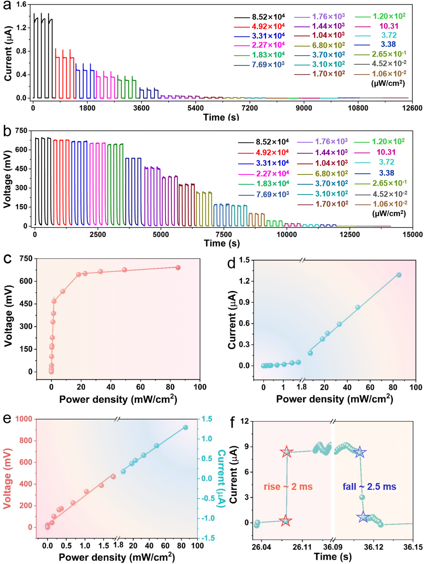 | ||
| Fig. 3 The performance of the device under 365 nm UV irradiation with different light intensities. (a) I–t curves under 365 nm UV light with various light intensities. (b) V–t curves under 365 nm UV light with various light intensities. (c) Segmented fitted curves of the voltage variation with UV light intensities. (d) Segmented fitted curves of the current variation with UV light intensities. (e) Fitted curves of the voltage and current with various UV light intensities. (f) Response time and recovery time of the self-powered UV photodetector ITO/BNT/LNO/glass under 365 nm light. | ||
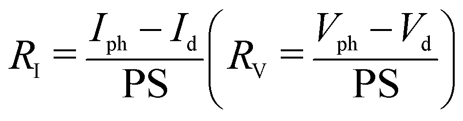
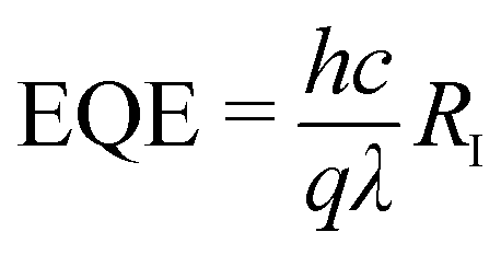
In this section, the key parameters of the photodetector, such as response time, responsivity (R), specific detectivity (D*), and external quantum efficiency (EQE), were also systematically investigated. The response time (time to raise the current from 10% to 90%) and recovery time (time to drop the current from 90% to 10%) of a self-powered photodetector were measured by periodically turning on and off the 365 nm light. The response time of the device was about 2 ms, and the recovery time was around 2.5 ms, as shown in Fig. 3f, which were substantially faster than the response time of the previously reported ZnO photodetectors (about roughly seconds).34 For the purpose of characterizing the photosensitivity of the ITO/BNT/LNO/glass self-powered UV photodetector to 365 nm light, the responsiveness of a photodetector can be calculated as a function of the current and light intensity, and the calculation formula is as follows:
where q denotes the charge of an electron.38 In Fig. S9a (ESI†), except for the point where the responsivity was zero, the value of RI did not change much throughout the light-intensity interval, and the change of
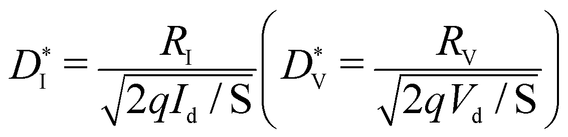
 was almost the same as that of RI. It is shown in Fig. S9b (ESI†) that RV decreased rapidly with increasing light intensity and then remained almost constant, and
  had a similar trend to RV. It can be distinctly seen from Fig. S9a and b (ESI†) that the responsiveness RI and the specific detection rate
  for the current did not vary much in the entire light-intensity range. However, for the voltage responsiveness RV and specific detection rate
  , the values of
  and RV in weak light were much larger than those in strong light. This indicates that the ITO/BNT/LNO/glass photodetector was well adapted to detect the weak 365 nm UV light. Also, under a faint UV light (4.52 × 10⁻² μW cm−2), the detector responsiveness and specific detection rate could reach 2.77 × 10⁵ V W−1 and 1.38 × 10¹⁴ Jones, respectively. Also, the values of
  and RI were much larger than those of a UV photodetector with a pyroelectric effect-enhanced ferroelectric barium titanate material.39 To further demonstrate that the detector was more suitable for UV light detection, a curve of the responsivity versus different wavelengths was tested, and the results proved that the detector had the highest responsivity to 365 nm UV light, compared to other wavelengths (Fig. S10, ESI†). EQE is a metric used to assess a PV device's energy conversion efficiency. As a result, EQE can serve as a reliable indicator of self-powered performance. The formula for calculating EQE is as follows:
where h is Planck's constant, λ represents incident light wavelength, and c stands for the speed of light.40 The value of EQE fluctuated slightly in the range of light intensity from 1.06 × 10⁻² μW cm−2 to 8.52 × 10⁴ μW cm−2, which was approximately 0.14% (Fig. S9c, ESI†). Table 1 summarizes the key parameters of self-powered UV photodetectors in recent years. The performance parameters of our detector were better than most the reported photodetectors based on a single ferroelectric material,26,41–45 and even better than the heterojunction photodetectors based on a combination of semiconductor and ferroelectric materials.22,27,28 The superior performance of our device was also comparable to some semiconductor-based photodetectors as well as some newly developed van der Waals heterojunction photodetectors and TiO2-based photodetectors.46,47 This suggests that the current–voltage dual-index probing method is a promising way to improve the device performance.
| Device | Wavelength (nm) | Lowest light intensity | Responsivity | D* (Jones) | Rise/decay time | Ref. |
|---|---|---|---|---|---|---|
| ITO/BTO/ITO | 405 | 4.3 mW cm−2 | ∼10−7 A W−1 | ∼105 | 0.6 s/0.5 s | 41 |
| ITO/BTO/Ag | 405 | 3.5 mW cm−2 | ∼10−7 A W−1 | ∼105 | 0.4 s/1.6 s | 42 |
| ITO/BTO/Ag | 405 | 7.78 mW cm−2 | 7.5 × 10⁻⁶ A W−1 | 8.5 × 10⁹ | 0.88 s/1.06 s | 43 |
| Ag/BFO/ITO | 365 | 45 μW cm−2 | 2.23 mA W−1 | 5.13 × 10⁷ | — | 44 |
| Au/BFO/Pt/TiO2/SiO2/Si | 340 | 720 μW cm−2 | 2.39 mA W−1 | 2.2 × 10¹⁰ | 420 ms/— | 24 |
| Au/PZT/FTO | 325 | 7.4 μW cm−2 | 0.092 A W−1 | 1.2 × 10¹² | 115 ms/178 ms | 45 |
| Au/PLZT/FTO | 340 | 0.1 mW cm−2 | 1.12 × 10⁻⁵ A W−1 | 4.43 × 10⁸ | 98 ms/96 ms | 26 |
| ITO/NiO/PLZT/FTO | 350 | 0.1 mW cm−2 | 6.3 × 10⁻⁴ A W−1 | 1.29 × 10¹⁰ | 0.34 s/0.36 s | 28 |
| Au/ZnO/PLZT/FTO | 360 | 40 mW cm−2 | 3.96 × 10⁻³ A W−1 | 6.6 × 10¹⁰ | 0.04 s/0.05 s | 27 |
| TiO2/PC71BM/PEDOT:PSS | 350 | 108 μW cm−2 | 33 mA W−1 | 1.6 × 10¹¹ | 60 ms/<1 μs | 46 |
| Ti3C2Tx/GaN | 355 | 30 μW cm−2 | 284 mA W−1 | 1.38 × 10¹³ | 7.55 μs/1.67 ms | 47 |
| ITO/BNT/LNO | 365 | 120 μW cm−2 | 5.67 × 10⁻⁴ A W−1 | 3.68 × 10⁹ | 2 ms/2.5 ms | This work |
| 45.2 nW cm−2 | 2.77 × 10⁵ V W−1 | 1.38 × 10¹⁴ |
2.4 Application of the ITO/BNT/LNO/glass self-powered UV photoelectric detector
Aiming to describe some promising applications of the ITO/BNT/LNO/glass photodetector, a self-powered photodetector array was constructed to detect the 365 nm light distribution by monitoring the output voltage signal in real time. Fig. 4a shows a photograph of the 3 × 3 ITO/BNT/LNO/glass photodetector under 365 nm UV light, where the size of each ITO electrode was 2 mm × 2 mm. The schematic of the ITO/BNT/LNO/glass photodetector array is given in Fig. 4b. A 3 × 3 matrix of ITO electrodes was deposited on the BNT thin film, and each electrode was linked to a grounded external load resistor. The output voltage signals of the nine channels were recorded concurrently in real time by using a multi-channel test system. By using a mask plate, 365 nm UV light with different light intensities was irradiated to some pixels of the 3 × 3 ITO/BNT/LNO/glass array, and large voltage signals could be seen on the mapping map of the lighted pixels as a result. Three different light intensities of 85.2, 1.44, and 0.12 mW cm−2 were irradiated on to the 3 × 3 ITO/BNT/LNO/glass device by using a “T” shaped mask plate, as shown in Fig. 4c–e. Three distinct “T” shaped voltage outputs were obtained on the mapping diagram. When the whole device was periodically irradiated with 365 nm UV light, each pixel presented a similar voltage signal as the light turning on and off, showing the homogeneity of these nine pixels, and the output voltage of each pixel increased as the light intensity increased (Fig. 4f and g). The output signal of each pixel was independent, which proved the dependability of the 3 × 3 ITO/BNT/LNO/glass array. Mask plates with different shapes were also designed and the “1”, “+”, and “L” shaped voltage outputs were obtained at the mentioned three different light intensities (Fig. S11, ESI†). Under 365 nm ultraviolet light intensity of 85.2, 1.44, and 0.12 mW cm−2, the corresponding V–t curves of “T”, “+”, “L”, and “1” shaped voltage outputs are described in Fig. S12a–d, S13a–d and S14a–d (ESI†). The feasibility of the device for UV photodetection was further demonstrated by these mapping plots.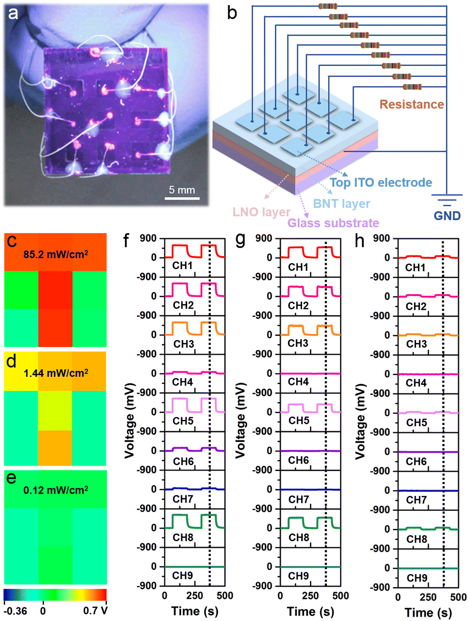 | ||
| Fig. 4 Application of the ITO/BNT/LNO/glass photodetector array. (a) Photograph of the ITO/BNT/LNO/glass photodetector array irradiated with 365 nm UV light. (b) Schematic diagram of the ITO/BNT/LNO/glass photodetector array structure. (c–e) “T” shaped pixels irradiated with 365 nm UV light at light intensities of 85.20 mW cm−2, 1.4 mW cm−2, and 0.12 mW cm−2, respectively. (f–h) V–t curves of the “T” shaped pixels under UV light intensities of 85.20 mW cm−2, 1.4 mW cm−2, and 0.12 mW cm−2, respectively. | ||
In addition, the curves of the current and voltage versus time for the nine channels were measured at the same light intensity, respectively (Fig. S15 and S16, ESI†). Fig. S15a–i (ESI†) show the variation curves of the voltage with time for the nine channels, respectively. Fig. S15j (ESI†) compares the magnitude of the tip voltage for the nine channels, and Fig. S15k (ESI†) compares the magnitude of the plateau voltage for the nine channels. Fig. S16a–i (ESI†) show the plots of the current versus time for nine channels. Fig. S16j (ESI†) compares the magnitude of the tip currents for the nine channels, and Fig. S16k (ESI†) compares the magnitude of the plateau currents for the nine channels. From these figures, it can be seen that the values of the current and voltage did not differ significantly for all the channels, except channel 1, which demonstrated the homogeneity of the device and the feasibility of using it for self-powered photodetector arrays.
3. Conclusion and outlook
It is generally said that conventional UV photodetectors mostly need an external bias power supply as a driving force to produce the photocurrent and prevent the compounding of photogenerated carriers,48 thereby limiting their miniaturization and integration in larger devices. Nevertheless, for wide-bandgap ferroelectric materials, their internal depolarization field can facilitate the separation of photogenerated charges. As a result, they may open up the possibility for developing self-powered photodetectors that do not require external power to overcome the constraints of integrated circuit technology.In this work, a BNT thin film was prepared by the sol–gel method and an ITO/BNT/LNO/glass self-powered photodetector was fabricated to detect UV light intensity. This device could detect 45.2 nW cm−2 of extremely weak UV light. The specific detection rate  and responsiveness RV under this weak UV light intensity were improved by 6585 and 1390 times, respectively, compared with strong UV light of 85.2 mW cm−2. It was obvious that the self-powered UV detector was more ideal for the detection of weak light. Furthermore, this detector had a reaction time of only 2 ms, which was significantly quicker than ferroelectric thin film-based photodetectors and some semiconductor photodetectors previously reported.25,49–52 What is more interesting is that the detector achieved UV light intensity detection over a wide linear detection range by using a current and voltage dual-indicators detection method. When the UV light intensity was less than 1.8 mW cm−2, the voltage was utilized to detect the light signal, When the UV light intensity was more than 1.8 mW cm−2, the current was used to detect the light signal. Based on this current and voltage dual-indicators detection mode, on the one hand, it can expand the detection range of UV light intensity, and on the other hand, it also allows the detector to maintain a relatively high sensitivity over the entire detection range.
In conclusion, a high-performance self-powered UV photodetector based on a BNT thin film was successfully prepared by using a simple method and at low cost to overcome the difficulties of using ferroelectric thin films for photodetectors without violating the concept of environmentally friendly development. Also, it used a double-indicators detection method to achieve a wide linear detection range of ultraviolet light intensities. Such a work will move forward the use of ferroelectric thin films in the field of photodetectors, and provide new ideas and thoughts for making detectors to detect weak light. It is trusted that the bandgap of ferroelectric films will be reduced by optimizing the preparation process of the films and doping modifications in subsequent research, so that they can be used to detect a wide spectrum from UV to visible light. Also, it can be expected that flexible substrates, such as mica, may be selected to make flexible photodetectors to provide more convenience for human life.
4. Experimental section
4.1 Synthesis of the sol
Preparation of BNT solution: As shown in Fig. S17a (ESI†), a certain molar ratio of bismuth nitrate pentahydrate and sodium nitrate was dissolved in pure water, ethanol, and glacial acetic acid, and stirred at 70° until the solution was clarified to obtain solution 1. Then a certain amount of tetrabutyl titanate, glacial acetic acid, acetylacetone, and ethanol were taken in a container and stirred for 30 min at room temperature to make solution 2. Then, solution 2 was added to solution 1 drop by drop, and then the mixed solution was stirred for 4 h at ambient temperature and aged for 24 h to obtain 0.1 mol L−1 clarified light-yellow BNT soliquid.Preparation of LNO solution: As in Fig. S17b (ESI†), a certain proportion of lanthanum nitrate and nickel acetate was dissolved in glacial acetic acid and pure water, and a clarified solution was obtained after stirring. Then, formamide was added to it and stirring was continued to obtain a clear green solution of 0.3 mol L−1.
4.2 Fabrication of the device
Preparation of BNT photovoltaic device: The FTO glass was put into a beaker and glass cleaner, deionized water, and ethanol were added and sonicated for 5 min, respectively, and then the solution was blow dried to remove the ethanol on the surface of the FTO glass with an air compressor. The FTO glass was placed in a homogenizer, and the LNO solution was spin-coated onto the FTO glass. Each wet film was dried at 180 °C for 3 min, pyrolyzed at 450 °C for 10 min, and finally annealed at 700 °C for 5 min. The above process was done 10 times to make the LNO electrode. The BNT solution was spin-coated onto the LNO electrode at 4000 rpm for 30 s. Each wet film was dried for 5 min at 100 °C, and then pyrolyzed for 5 min at 400 °C. After the above procedure was performed 12 times, the film was annealed at 700 °C for 30 min. The ITO electrodes were deposited on the BNT/LNO/glass by RF magnetron sputtering at 150 W. Finally, the ITO/BNT/LNO/glass photovoltaic device was obtained.4.3 Characterization and measurements
Characterization of BNT photovoltaic devices: the surface microstructure of BNT thin film was characterized by field emission scanning electron microscopy (Nova NanoSEM 450), as well as the thickness of the ITO/BNT/LNO thin film was observed. The crystal structure of a BNT thin film was analyzed by XRD with Cu Kα radiation (XRD, PANalytical X'Pert3 Powder). Atomic force microscopy (AFM, Bruker, Dimension Icon) in knockdown mode was used to characterize the surface morphology of the BNT thin film.Electrical measurements: a UV-Vis spectrophotometer (Ultra-6600A, RIGOL) was used to acquire the absorption and transmission spectra. The output voltage, current as well as the I–V characteristic curves of the BNT device were tested utilizing a Keithley 2611B system. Moreover, different wavelengths of light irradiated the device using a multi-channel light-emitting diode lighting system, and the light sources were fixed at specific locations to maintain the same light intensity for different wavelengths. By placing varying neutral density filters between the device and the 365 nm UV light, the intensity of the 365 nm light could be adjusted. Also, the light intensity was measured by a power meter (OPHIR, PD300-UV; OPHIR, PD300-1W). The output voltage signal of the ITO/BNT/LNO/glass 3 × 3 matrix array was measured simultaneously with a multi-channel data acquisition system (NI PXIe-6358).
Conflicts of interest
There are no conflicts to declare.Acknowledgements
This work was supported by the National Natural Science Foundation of China (Grant No. 52072041), the Beijing Natural Science Foundation (Grant No. JQ21007), and the University of Chinese Academy of Sciences (Grant No. Y8540XX2D2).References
- P. J. Li, Z. M. Liao, X. Z. Zhang, X. J. Zhang, H. C. Zhu, J. Y. Gao, K. Laurent, Y. Leprince-Wang, N. Wang and D. P. Yu, Nano Lett., 2009, 9, 2513–2518 CrossRef CAS PubMed.
- R. Zou, Z. Zhang, Q. Liu, J. Hu, L. Sang, M. Liao and W. Zhang, Small, 2014, 10, 1848–1856 CrossRef CAS PubMed.
- Y. Fang, Q. Dong, Y. Shao, Y. Yuan and J. Huang, Nat. Photonics, 2015, 9, 679–686 CrossRef CAS.
- X. Han, W. Du, R. Yu, C. Pan and Z. L. Wang, Adv. Mater., 2015, 27, 7963–7969 CrossRef CAS PubMed.
- Q. Lin, A. Armin, P. L. Burn and P. Meredith, Nat. Photonics, 2015, 9, 687–694 CrossRef CAS.
- N. Youngblood, C. Chen, S. J. Koester and M. Li, Nat. Photonics, 2015, 9, 247–252 CrossRef CAS.
- H. Chen, H. Liu, Z. Zhang, K. Hu and X. Fang, Adv. Mater., 2016, 28, 403–433 CrossRef CAS PubMed.
- X. Yu, T. J. Marks and A. Facchetti, Nat. Mater., 2016, 15, 383–396 CrossRef CAS PubMed.
- X. Fang, L. Hu, K. Huo, B. Gao, L. Zhao, M. Liao, P. K. Chu, Y. Bando and D. Golberg, Adv. Funct. Mater., 2011, 21, 3907–3915 CrossRef CAS.
- K. O. Boltar, I. D. Burlakov, V. P. Ponomarenko, A. M. Filachev and V. V. Salo, J. Commun. Technol. Electron., 2016, 61, 1175–1185 CrossRef.
- W. Mou, L. Zhao, L. Chen, D. Yan, H. Ma, G. Yang and X. Gu, Solid-State Electron., 2017, 133, 78–82 CrossRef CAS.
- S. K. Samanta, S. Chatterjee, W. K. Choi, L. K. Bera, H. D. Banerjee and C. K. Maiti, Semicond. Sci. Technol., 2003, 18, 33–38 CrossRef CAS.
- F. X. Liang, D. Y. Zhang, J. Z. Wang, W. Y. Kong, Z. X. Zhang, Y. Wang and L. B. Luo, Opt. Express, 2016, 24, 25922–25932 CrossRef CAS PubMed.
- Y. Xie, L. Wei, G. Wei, Q. Li, D. Wang, Y. Chen, S. Yan, G. Liu, L. Mei and J. Jiao, Nanoscale Res. Lett., 2013, 8, 188 CrossRef PubMed.
- G. Ma, W. Jiang, W. Sun, Z. Yan, B. Sun, S. Li, M. Zhang, X. Wang, A. Gao, J. Dai, Z. Liu, P. Li and W. Tang, Phys. Scr., 2021, 96, 125823 CrossRef.
- Z. Liu, S. H. Zhang, Y. S. Zhi, S. Li, Z. Y. Yan, X. L. Chu, A. Bian, P. G. Li and W. H. Tang, J. Phys. D: Appl. Phys., 2021, 54, 195104 CrossRef CAS.
- Y. Lee, I. Omkaram, J. Park, H.-S. Kim, K.-U. Kyung, W. Park and S. Kim, IEEE Electron Device Lett., 2015, 36, 41–43 CAS.
- D. Yang and D. Ma, Adv. Opt. Mater., 2019, 7, 1800522 CrossRef.
- Q. Zhang, H. Li, Y. Ma and T. Zhai, Prog. Mater. Sci., 2016, 83, 472–535 CrossRef CAS.
- S. Zhao, H. P. T. Nguyen, M. G. Kibria and Z. Mi, Prog. Quantum Electron., 2015, 44, 14–68 CrossRef.
- C. O. Kim, S. Kim, D. H. Shin, S. S. Kang, J. M. Kim, C. W. Jang, S. S. Joo, J. S. Lee, J. H. Kim, S. H. Choi and E. Hwang, Nat. Commun., 2014, 5, 3249 CrossRef PubMed.
- X. Yu, S. Zhang, H. Zeng and Q. J. Wang, Nano Energy, 2016, 25, 34–41 CrossRef CAS.
- R. Gupta, M. Tomar and V. Gupta, presented in part at the International Workshop on Thin Films for Electronics, Electro-Optics, Energy and Sensors, 2015, 9667, 966703.
- P. P. Biswas, S. Pal, V. Subramanian and P. Murugavel, J. Phys. D, 2020, 53, 275302 CrossRef CAS.
- L. Su, H. Y. Li, Y. Wang, S. Y. Kuang, Z. L. Wang and G. Zhu, Nano Energy, 2017, 31, 264–269 CrossRef CAS.
- J. Chen, A. S. Priya, D. You, W. J. Pei, Q. F. Zhang, Y. M. Lu, M. K. Li, J. M. Guo and Y. B. He, Sens. Actuators, A, 2020, 315, 112267 CrossRef CAS.
- J. Chen, Z. H. Wang, H. F. He, J. X. Mao, Y. Zhang, Q. F. Zhang, M. K. Li, Y. M. Lu and Y. B. He, Adv. Electron. Mater., 2021, 7, 2100717 CrossRef CAS.
- J. Chen, D. You, Y. Zhang, T. Zhang, C. Yao, Q. F. Zhang, M. K. Li, Y. M. Lu and Y. B. He, ACS Appl. Mater. Interfaces, 2020, 12, 53957–53965 CrossRef CAS PubMed.
- K. Song, N. Ma and Y. Yang, Adv. Mater. Technol., 2017, 2, 1700221 CrossRef.
- L. Li, M. Li, H. Zhang, I. M. Reaney and D. C. Sinclair, J. Mater. Chem. C, 2016, 4, 5779–5786 RSC.
- W. Sakamoto, N. Makino, T. Katayama, M. Moriya and T. Yogo, Ferroelectrics, 2015, 479, 56–63 CrossRef CAS.
- R. Zhao, N. Ma, J. Qi, Y. K. Mishra, R. Adelung and Y. Yang, Adv. Electron. Mater., 2019, 5, 1800791 CrossRef.
- T.-H. Yang, Y.-W. Harn, K.-C. Chiu, C.-L. Fan and J.-M. Wu, J. Mater. Chem., 2012, 22, 17071 RSC.
- B. Ouyang, K. Zhang and Y. Yang, Adv. Mater. Technol., 2017, 2, 1700208 CrossRef.
- C. Paillard, X. F. Bai, I. C. Infante, M. Guennou, G. Geneste, M. Alexe, J. Kreisel and B. Dkhil, Adv. Mater., 2016, 28, 5153–5168 CrossRef CAS PubMed.
- A. Bhatnagar, A. R. Chaudhuri, Y. H. Kim, D. Hesse and M. Alexe, Nat. Commun., 2013, 4, 2835 CrossRef.
- K. Song, N. Ma, Y. K. Mishra, R. Adelung and Y. Yang, Adv. Electron. Mater., 2019, 5, 1800413 CrossRef.
- J. Qi, N. Ma and Y. Yang, Adv. Mater. Interfaces, 2018, 5, 1701189 CrossRef.
- N. Ma and Y. Yang, Nano Energy, 2017, 40, 352–359 CrossRef CAS.
- B. S. Ouyang, C. Chang, L. D. Zhao, Z. L. Wang and Y. Yang, Nano Energy, 2019, 66, 104111 CrossRef CAS.
- N. Ma and Y. Yang, Nano Energy, 2018, 50, 417–424 CrossRef CAS.
- N. Ma, K. W. Zhang and Y. Yang, Adv. Mater., 2017, 46, 1703694 CrossRef PubMed.
- K. Zhao, B. S. Ouyang, C. R. Bowen and Y. Yang, Nano Energy, 2020, 77, 105152 CrossRef CAS.
- R. D. Zhao, N. Ma, K. Song and Y. Yang, Adv. Funct. Mater., 2020, 30, 1906232 CrossRef CAS.
- M. M. Chen, X. M. Shen, C. Zhou, D. W. Cao and W. Xue, J. Alloys Compd., 2022, 897, 163208 CrossRef CAS.
- T. T. Yan, S. Cai, Z. J. Hu, Z. Q. Li and X. S. Fang, J. Phys. Chem. Lett., 2021, 12, 9912–9918 CrossRef CAS PubMed.
- W. D. Song, J. X. Chen, Z. L. Li and X. S. Fang, Adv. Mater., 2021, 33, 2101059 CrossRef CAS PubMed.
- E. A. Mojtabavi and S. Nasirian, Opt. Mater., 2019, 94, 28–34 CrossRef CAS.
- P. Mukhopadhyay and W. V. Schoenfeld, J. Vac. Sci. Technol., A, 2020, 38, 013403 CrossRef CAS.
- A. H. Ahmad Makinudin, O. Al-Zuhairi, A. Anuar, M. Z. Zainorin, A. S. Abu Bakar, S. DenBaars and A. Supangat, Mater. Lett., 2021, 286, 129244 CrossRef CAS.
- F. Abbasi, F. Zahedi and M. H. Yousefi, Opt. Commun., 2021, 482, 126565 CrossRef CAS.
- L. Su, S.-Y. Chen, L. Zhao, Y. Zuo and J. Xie, Appl. Phys. Lett., 2020, 117, 211101 CrossRef CAS.
Footnote |
| † Electronic supplementary information (ESI) available. See DOI: https://doi.org/10.1039/d2nh00204c |
| This journal is © The Royal Society of Chemistry 2022 |