
Neuromorphic behaviour in discontinuous metal films†
Saurabh K.
Bose
 a,
Joshua B.
Mallinson
a,
Edoardo
Galli
a,
Susant K.
Acharya
a,
Chloé
Minnai
b,
Philip J.
Bones
c and
Simon A.
Brown
*a
a,
Joshua B.
Mallinson
a,
Edoardo
Galli
a,
Susant K.
Acharya
a,
Chloé
Minnai
b,
Philip J.
Bones
c and
Simon A.
Brown
*a
aThe MacDiarmid Institute for Advanced Materials and Nanotechnology, School of Physical and Chemical Sciences, University of Canterbury, Christchurch, New Zealand. E-mail: simon.brown@canterbury.ac.nz
bMolecular Cryo-Electron Microscopy Unit, Okinawa Institute of Science and Technology Graduate University, 1919-1 Tancha, Onna-son, Kunigami-gun, Okinawa, Japan
cElectrical and Computer Engineering, University of Canterbury, Private Bag 4800, Christchurch 8140, New Zealand
First published on 1st March 2022
Abstract
Physical systems that exhibit brain-like behaviour are currently under intense investigation as platforms for neuromorphic computing. We show that discontinuous metal films, comprising irregular flat islands on a substrate and formed using simple evaporation processes, exhibit correlated avalanches of electrical signals that mimic those observed in the cortex. We further demonstrate that these signals meet established criteria for criticality. We perform a detailed experimental investigation of the atomic-scale switching processes that are responsible for these signals, and show that they mimic the integrate-and-fire mechanism of biological neurons. Using numerical simulations and a simple circuit model, we show that the characteristic features of the switching events are dependent on the network state and the local position of the switch within the complex network. We conclude that discontinuous films provide an interesting potential platform for brain-inspired computing.
New conceptsNetworks of nanoscale components exhibit a variety of brain-like properties and therefore may be important for applications in neuromorphic computing. Neuromorphic networks are usually formed by deposition of pre-formed nanowires or nanoparticles. Here we demonstrate brain-like behaviour in discontinuous films, which are networks of nanoscale islands that self-assemble during atomic deposition processes. The discontinuous films exhibit novel switching behaviour that leads to the observation of avalanches of neuron-like electrical signals. The avalanches provide evidence of critical states that are believed to be optimal for information processing. The experiments are supported by simulations that reveal the impact of the equivalent electrical circuit for the network on the observed behaviour. Since discontinuous films can be made using any standard evaporative coating system, these results open the way to widespread utilisation of discontinuous films in neuromorphic computing. |
Introduction
Discontinuous films (DFs) are nanostructured metallic films that are typically formed via self-assembly during simple atomic deposition processes. In the 1970s and 1980s DFs were studied extensively (for reviews see ref. 1, 2) because – in the era before nanotechnology became a central focus for scientific research – they provided a convenient and easily fabricated nanoscale system. There has been ongoing interest in DFs (and related granular films3) but the relative ease of modern fabrication techniques has meant that emphasis has generally shifted toward more precisely controlled structures and devices.Among these are a number of different technologies which aim to reproduce some aspect of the structure or function of the brain.4–7 A worldwide effort in this direction is driven by both the limitations of existing computing technologies and by the recognition that the brain is extremely efficient in processing certain types of information. Neuromorphic devices include large scale integrated circuits8–10 with precise CMOS designs for individual neurons and elaborate architectures to interconnect them. These architectures have been successful in enabling, for example, fast matrix multiplication algorithms,5 pattern recognition8 and autonomous control of a vehicle,10 but development costs remain high, and achievement of truly brain-like architectures is challenging.
An alternative approach has been to develop self-assembled networks of nanoscale components, where the intrinsic physics provides brain-like structure and/or function. More particularly, it has been proposed that the structures of self-assembled networks of nanowires and nanoparticles mimic some of the complex biological structures of the brain, and therefore may be useful as novel systems for neuromorphic computing.11–15 For example, percolating networks of nanoparticles have been demonstrated to provide intrinsically scale-free architectures16 and exhibit dynamical behavior that is comparable to that of the biological cortex.14 These complex all-metal self-assembled networks exhibit interesting memristor-like switching behaviour17–22 and correlations that are promising23–25 for realizing brain-inspired computational approaches such as reservoir computing (RC).26–28 RC is just one of many possible approaches, but it is a useful example because of its conceptual simplicity and because recent successful demonstrations in nanoscale networks29–32 mean that the approach is becoming well-established. The basic concept is that a reservoir of highly interconnected non-linear nodes (which evolve dynamically in response to input signals) can be used to map input signals onto outputs of higher dimensions, which are then examined by an external readout function in order to perform a variety of tasks. Only output weights are trained, using simple matrix inversion techniques, ensuring that training is fast and cheap.26,27
An important target for more general approaches to neuromorphic computing is the realisation of devices that exhibit criticality. The brain is believed to be poised at a critical point,33,34 which is significant as critical dynamics are associated with an optimal capability for information processing.35 To date, percolating networks of Sn nanoparticles are the only neuromorphic platforms in which criticality has been unambiguously demonstrated.14 In order to move towards applications it is important to determine what attributes of the devices are essential for criticality. The literature36 suggests that the scale-free nature of the network is important but criticality has been tentatively observed in nanowire networks which have other architectures.15,29 Additionally, the optimal material for device fabrication is not yet clear and there are likely to be tradeoffs between different material properties e.g. Sn particles14 are advantageous in that they are easily produced, but they are prone to oxidation which may limit real-world applications. Other materials and network architectures should therefore be explored. The results presented here are the first confirmation of critical behaviour in a nanoparticle network that is stable in ambient conditions. This, coupled with a simple fabrication procedure, makes DFs attractive for real world applications.
One of the attractions of using pre-defined nanoparticles for device fabrication is that they provide control over the resulting morphology.18,19,21 However the coalescence of the particles after deposition often means that the resulting morphologies have some similarities with those of discontinuous films, providing one of the key motivations for the present work. Here we show that DFs can have similar electrical characteristics to neuromorphic devices built from networks of nanoparticles. More particularly we show that with careful control of the deposition process it is possible to achieve stable devices through atomic-scale self-assembly. The devices exhibit complex brain-like avalanches of electrical activity, and meet many of the criteria for criticality.14,33,34 We discuss the switching mechanisms in DFs in detail and highlight in particular that switching results from neuron-like integrate-and-fire behaviour. We also demonstrate a surprising inversion of the measured sign of changes in conductance caused by switching events. We use simulations to show that this inversion can be understood as a consequence of changes in the connectivity of the network that modify its equivalent circuit.
Recent work on DFs has focused on the physics of the formation of the nanostructures37–40 as well as a range of applications such as biosensors,41 chemical sensors,42,43 temperature dependent resistors,44 and strain gauges.45,46 It is commonly observed that such films can exhibit extremely poor conductivities compared to normal metals47 (and even metal-insulator transitions38,48) and understanding the electron transport in such discontinuous granular systems remains challenging.3 Nevertheless it is clear that the general properties of such films can be understood within the framework of percolation theory.17,49,50 To our knowledge there has been no previous study of the potential neuromorphic properties of DFs, and we believe that the present work may excite a new wave of interest in DFs which are conveniently fabricated in any laboratory equipped with a standard evaporator.
Results and discussion
Our discontinuous films are prepared by evaporation of gold onto Si3N4/Si substrates which have 2 predefined electrodes with separation 100 μm. We fabricated more than 100 devices which all show similar behaviour, but for coherency present representative data from three devices (devices A–C). Supporting data from three additional devices (devices D–F) are included in the ESI.†Fig. 1a shows the resistance of typical devices during the deposition process, with an approximately exponential dependence on the thickness of the deposited gold. Fig. 1b shows that the stability of the devices depends sensitively on the selected resistance at the end of the deposition process (Rdep). We find that for deposition rates ∼0.3–1 nm min−1 and Rdep ∼0.3 MΩ it is possible to achieve devices that are stable over long periods of time (Fig. S1, ESI† shows data over 200 hours), and which have the well-controlled morphology shown in the inset of Fig. 1a. For higher (lower) values of Rdep the resistance is observed to increase (decrease) continuously and the devices are unstable, and quickly reach resistance ranges in which interesting effects cannot be observed.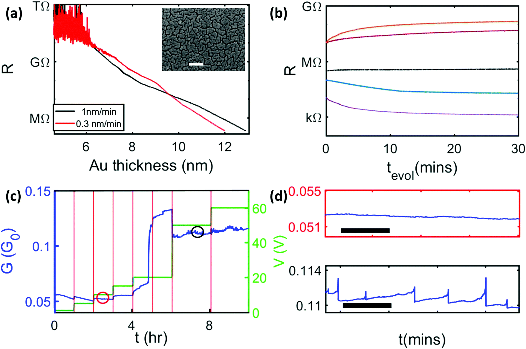 | ||
| Fig. 1 Discontinuous film fabrication and activation of switching. (a) Resistance as a function of film thickness for two different deposition rates. Atomic deposition of Au films between pre-formed electrodes is terminated when Rdevice reaches Rdep ∼0.2 MΩ (Au thickness ∼12.5 nm), which results in the discontinuous film structure shown in the SEM micrograph (inset). Scale bar is 200 nm. (b) Surface energy induced post-deposition restructuring (coalescence) results in an increase in Rdevice for Rdep ≳ 0.5 MΩ and a decrease in Rdevice when Rdep ≲ 0.1 MΩ. Here a small read voltage (100 mV) is applied across the device. For optimum Rdep in the range ∼0.2–0.3 MΩ, Rdevice is stable over long periods of time (black curve). (c) Application of increasing voltage stimulus to device A with optimum Rdep leads to network activation marked by rapid increase in conductance G in units of G0 = 2e2/h (t ∼5 h here). (d) The top panel [zoomed in section from red circle in (c)], shows no switching before activation, whereas the bottom panel [zoomed in section from black circle in (c)] shows that after network activation the device shows interesting switching events. The black scale-bars are 5 mins. | ||
After deposition the applied voltage is increased in a series of steps resulting in initial ‘forming’ behaviour, i.e. changes in morphology (local restructuring of tunnel gaps across the film) that lead to the switching behaviour of interest. In the example shown in Fig. 1c the conductance (G, in units of G0 = 2e2/h) increases by a factor of ∼3, after which switching behaviour is observed (Fig. 1d). Fig. S2 (ESI†) shows that the rate of switching is strongly dependent on the applied voltage. The forming behaviour and voltage dependence of the switching are similar to those observed in Au nanoparticle devices.19
Morphology
The key aspect of the device fabrication procedure is control of the morphology during the deposition, which results in nanoscale islands with well-defined tunnel gaps between them. The tunnel gaps then allow filament formation and consequent neuron-like behaviour. The important point is that when resistances in the range of ∼0.3 MΩ are achieved the size of the resulting islands, and the density of the tunnel gaps, is well-controlled. The resulting morphology of the Au discontinuous films (Fig. 1a, inset) is consistent with that of devices with the same thickness made in the same evaporator system a decade ago.42 While there are qualitative similarities (complex island structures separated by tunnel gaps) with the morphologies that result from the deposition of either tin14,17 or gold19 clusters, diffusion and coalescence of the deposited atoms leads to distinct differences in detail. DFs comprise Au islands that are much flatter and broader than those in Au nanoparticle devices and the DFs do not exhibit the highly ramified structures that are observed after deposition of clusters. Fig. S3 (ESI†) shows that the morphology of the films varies only slightly from device to device and we emphasise that, as for cluster deposited films, the islands are separated from each other by nanoscale tunnelling gaps.1,2,42 The qualitative and quantitative similarity (see details below) between the switching data obtained from the DFs and those obtained from cluster deposited devices suggests strongly that the mechanism for switching is the same i.e. that increases in conductance result from formation of atomic scale filaments in the tunnel gaps, and that decreases in conductance result from breaking the same filaments. These mechanisms are illustrated in Fig. 2 and have been discussed in detail elsewhere.16,51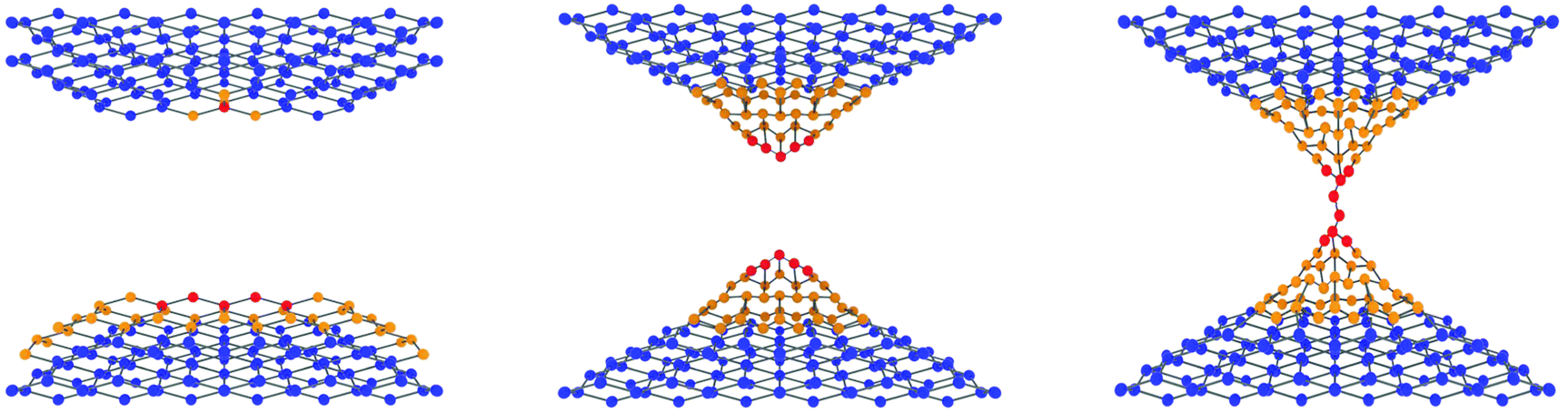 | ||
| Fig. 2 Schematic of the switching process. The electric field in the tunnel gap between two islands in the discontinuous film leads to formation of ‘hillocks’ of atoms, and subsequently to atomic scale filament formation. See text and ref. 14, 16 for details. | ||
Switching dynamics and temporal correlations
We now discuss brain-like correlated switching dynamics in the DFs. Fig. 3a shows typical switching behaviour over a timeframe of several hours (top panel: G; bottom panel: ΔG). Complex sequences of switching events are observed, with switching associated with atomic filament formation occuring at multiple different locations in the network.16 The devices exhibit similar patterns of switching behaviour over many days, whether in vacuum or ambient (see Fig. S4, ESI†). Fig. 3b shows that the switching events cause sharp changes in G that are qualitatively similar to those obtained from percolating tin devices14,17 and networks of gold nanoparticles.19,20 There are also however additional continuous changes in G between the sharp transitions (arrowed data segments in Fig. 3b; see also Fig. S5, ESI†) which will be discussed below.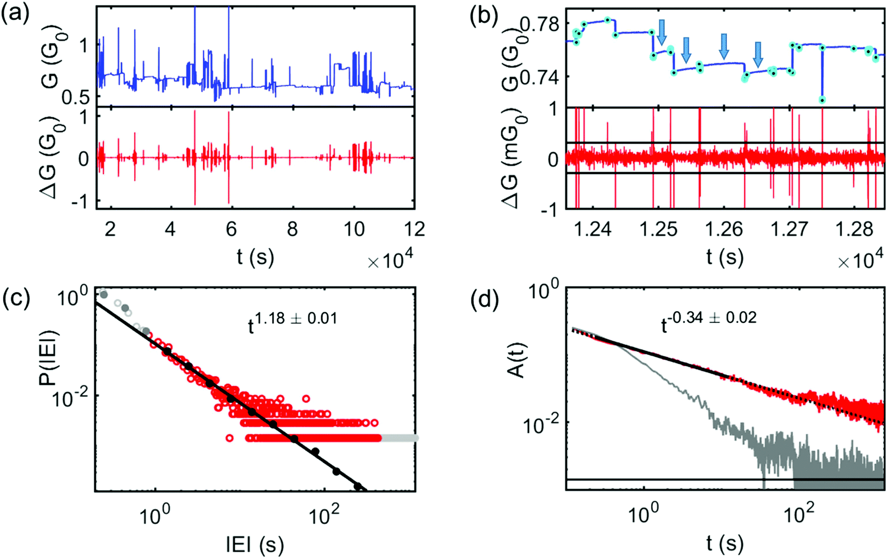 | ||
| Fig. 3 (a) Typical conductance switching data from device C, measured with fixed DC voltage = 20 V over multiple hours with 5 Hz sampling rates (see Methods), showing complex patterns of switching events and bursty dynamics. Network conductance (G, blue), and event size (ΔG, red) (b) A zoomed in portion of the data from (a), note the changes in both scales, demonstrating event detection (sharp changes in G). Marked events (filled circles) are those for which ΔG > ΔGth = 0.3 mG0 which is marked by the black horizontal lines (refer to ESI† for discussion of the choice of ΔGth). Several examples of continuous changes in G are marked with arrows, and discussed in the main text. (c) Distribution of inter-event intervals P(IEI) and autocorrelation function A(t) (red) in (d) are power law distributed with the fitted exponents similar to those observed in Sn cluster networks.14,16 Shuffled data25 show much weaker correlations (grey). | ||
Fig. 3c and d show that the distribution of inter-event intervals (IEIs) and the autocorrelation functions are power laws. There is reasonable quantitative agreement with the power law exponents observed in percolating tin devices (see Table S1, ESI†), consistent with switching mechanisms and network dynamics previously identified.16 The bursts of events evident in Fig. 3a are consistent with avalanches of switching: when one switch changes state it causes changes in the distribution of voltages in the network leading to further switching events at other sites (tunnel gaps). Avalanches are important characteristics of the dynamical behaviour of the biological brain, since when one neuron fires it is likely to trigger another. Following the methodology of ref. 14, 52 we show in Fig. S6 (ESI†) that both the sizes and durations of the avalanches are power law distributed, and present data in Table S2 (ESI†) that demonstrates that the avalanches are consistent with rigorous criteria for criticality.14,33,34 Hence, our discontinuous films exhibit avalanches of switching events that are qualitatively and quantitatively similar to avalanches of neurons firing in the brain.52,53 Criticality is believed to be a signature of special dynamics that allow optimal information processing,14,35 suggesting that DFs may provide a novel platform for neuromorphic algorithms such as reservoir computing.25,27
Switching characteristics: integrate and fire behaviour
Having discussed collective behaviour in the previous section, we now focus on individual switching events. Fig. 1d (lower panel) shows a typical series of events, each with a slow increase in conductance followed by a sudden drop. Fig. S7 (ESI†) shows individual events in more detail. This type of spiking behaviour can be viewed16 as representative of an atomic scale integrate-and-fire mechanism, analogous to one of the key characteristic behaviours of biological neurons.54,55 The atomic scale mechanism is discussed in more detail below, but we first turn to a more detailed discussion of the typical spiking characteristics, which can be broadly classified according to the conductance state of the samples. Fig. 4 compares typical individual switching events that are observed in low G and high G states (e and g respectively) and presents G(V) curves measured in those states (d and f respectively – see ESI† II for details on these measurements). In the low G state, the G(V) curves are approximately linear, with a modest increase in conductance (note that this corresponds to a slight non-linearity in the I(V) curves). In the high G state the G(V) curves are approximately parabolic, with a decrease in conductance with increasing V i.e. there is a strong negative curvature.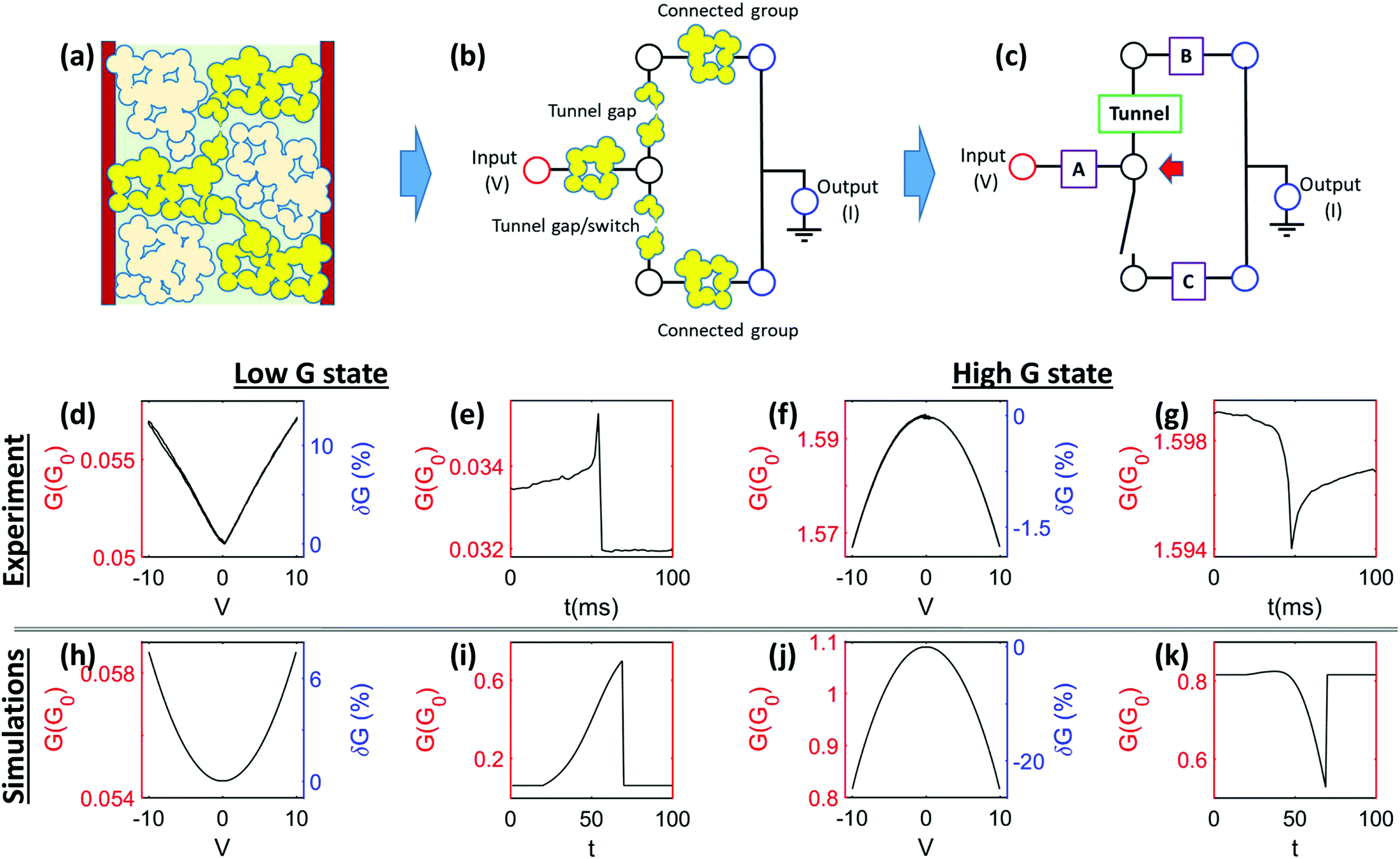 | ||
| Fig. 4 Minimal model to explain measured non-linear conductance changes in high G and low G states. (a) In the model, the complex network is modeled as three identical groups of Au islands (yellow) separated via tunnel gaps which transport current, and other parts of the network (beige) which are electrically isolated from the current path between the electrodes on the edges (red). (b) The modeled current path between the electrodes includes two tunnel gaps that separate groups of ohmically interconnected islands. The lower tunnel gap is assumed to be the site of the atomic scale switch that causes the transition between the low and high conductance states. The upper tunnel gap retains the same non-linearity throughout the simulation. (c) The groups are modeled as identical circuit elements A, B and C, which, because these elements are internally well-connected, are assumed to have the same non-linearity as the network in the high G state. (i.e. both the resistances and their voltage dependences are identical). (d–g) Experimental observations (for device B) (top row) and the numerical simulations (h–k, bottom row) are shown for both low and high G states. The panels show a good match between the experimental observations and the simulations. | ||
The key point in Fig. 4 (compare e and g), and in the further examples shown in Fig. S7 (ESI†), is that inverted switching characteristics are observed in the two states i.e. in low (high) G states the switching events typically appear as a continuous increase (decrease) in G followed by a sharp jump back close to the original value. Note that the continuous changes in G are intrinsic behaviour of the sample – the much faster responses to pulsed inputs in Fig. S8 (ESI†) show that capacitive time constants are much shorter (detailed investigations reveal τ ∼100 μs). Furthermore, similar continuous changes are observed at both slow and fast sampling rates (Fig. S7, ESI†).
In the low conductance state, the continuous increases in conductance are associated with growth of a ‘hillock’ of atoms on one or both sides of a tunnel gap16 (see Fig. 2), resulting from the strong electric field in the gap.17 The subsequent drop in conductance occurs when the growth of the hillock is completed, resulting in filament formation. The increase in conductance in turn causes an increase in current, which then breaks the filament and causes the conductance to fall back close to its original level i.e. the tunnel gap returns back to its original size (in many cases the final conductance is lower than the original one, suggesting a return to the original gap size, with no hillock). Continuous changes in G associated with hillock formation were observed previously for only a few switching events in Sn nanoparticle devices.16 In contrast, in DFs they are much more common – e.g. for every event in Fig. S5 (ESI†). Pulsed voltage measurements (Fig. 5) show that each pulse results in an increase in conductivity i.e. the integration of the applied voltage results in further growth of the ‘hillock’. The conductance does not drop between pulses showing that the hillock formed is robust on the timescale of the (short) pulse length. The hillocks are robust even if the bias is reversed, providing evidence that hillocks are in fact formed on both sides of the tunnel gap, as illustrated in Fig. 2. The hillock size depends on all previous voltage inputs (both the external ones, and those from the rest of the network) and so this atomic scale behaviour explains the observed integrate-and-fire mechanism.
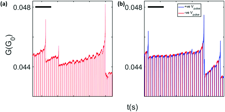 | ||
| Fig. 5 Switching behaviour in response to pulsed voltages – hillock formation followed by filament formation and breaking. (a) Conductance as a function of time for pulsed voltages. 50 V pulses were applied. 1 V read voltages allow the conductance to be monitored in between pulses. Continuous changes in G accumulate with each consecutive voltage pulse, consistent with integrate-and-fire (IF) behaviour.16 These measurements were performed on device E with pulse width τp = 100 ms and sampling intervals of 200 μs. Scale bars are 2 s in both panels. As the hillock relaxation in the tunnel gap is relatively slow, ‘leakiness’ is not observed. (b) Similar behaviour for bipolar pulses showing that hillock formation is independent of the polarity of the voltage stimulus.14,16 | ||
Numerical modelling
As noted above, the remarkable feature of Fig. 4g is that in the high G state the conductance changes during hillock formation are the opposite of those in the low G state (Fig. 4e) i.e. gradual decreases in G are followed by sharp increases in G. We believe that this inversion in behaviour is due to the changes in the effective electrical circuit that arise when the device switches from the low to high G states, as detailed in the following model.Fig. 4a shows a schematic of the DF film structure. The Au islands that form the current path between the electrodes (yellow) are shown within an equivalent circuit in Fig. 4b and c. The essential features of the network are the highly connected parts of the film A, B and C, and the two tunnel gaps that connect them in a series/parallel configuration. [The well-connected groups A, B, C each have high conductance (high G) and so these individual groups exhibit strong G(V) behaviour that is similar to that measured in the high conductance state of the network as a whole.] The lower tunnel gap acts as a switch which, when closed, causes the transition from the low G to high G state due to the additional current path. The upper tunnel gap is the site at which the growth of the atomic scale hillock leads to an increase in conductance of the gap, prior to formation of a completed filament. Obviously switching and hillock growth can occur at many different sites in the actual DF, but in each case a similar model and equivalent circuit can be applied.
When the different voltage dependencies of the components of the network are considered in the simple circuit model, the inversion of the switching characteristic naturally emerges (bottom row in Fig. 4 – for further detail see ESI† Section III). In essence the inversion occurs in the high G state because, when the conductance of the tunnel gap increases, additional voltage is dropped over parts of the network (specifically A) that have a strong negative curvature in G(V). Hence, the extra voltage causes the conductance of those parts of the network to drop. Thus, the network conductance drops in response to an increase in conductance of the upper junction: the simple circuit model accounts for the reversal in sign of the change in conductance, and can even lead to much bigger negative values of ΔG than are observed experimentally. We tested multiple different equivalent circuits and found that this series/parallel combination is the simplest which explains the observed data. Obviously more complex circuits are possible, but the introduction of additional circuit elements increases the number of adjustable parameters and makes agreement with the experiments less satisfying.
Finally we mention two additional features that are sometimes observed: (i) continuous changes in G between switching events (downward arrows in Fig. 3b) and (ii) gradual changes in conductance that seem to precede or follow clear switching events (Fig. S5 and S7, ESI†). In light of the above discussion it is clear that these are likely due to the changes in hillock height at other sites (tunnel gaps) within the network.
Conclusion
In summary, we have demonstrated that it is possible to fabricate discontinuous metal films which exhibit complex switching behaviour, so long as initial device resistances are within a narrow range (Rdep ∼0.3 MΩ). We have explored the detail of the atomic-scale switching mechanism and, using a simple circuit model, we have demonstrated a surprising inversion of the sign of the measured change in conductance that depends on the position of the switch within the network. The devices exhibit correlated, brain-like avalanches of electrical signals that are signatures of criticality. DFs therefore provide a potential new route towards energy-efficient brain-like computing which complements ongoing work on networks of nanowires and pre-formed particles.Recent demonstrations of RC in networks of nanowires29–32 as well as in other systems such as all optical networks56,57 confirm the potential of networks of brain-like components for information processing, and a next step in the field is to more carefully consider practical considerations such as power consumption and ease of fabrication. In the present (unoptimised) devices power consumption is in the range 10–100 mW, which is comparable to that in ref. 30 We expect that a reduction of the dimensions of the network would be advantageous in reducing both operating voltages and power consumption. One of the advantages of DFs is that they can be fabricated in almost any nanofabrication laboratory, in high vacuum conditions that ensure cleanliness and reliability. Furthermore, by monitoring the conductance of the devices during deposition, well-defined network architectures can be engineered (see next paragraph). Methods that rely on deposition of components from solution are generally considered to be less desirable from the point of view of standard CMOS fabrication techniques and are more difficult to control.
An important issue still to be resolved is the nature of the network comprising the gold islands that make up the DF (Fig. 1a and Fig. S3, ESI†), and in particular whether the network has a scale-free25 architecture. Ideally, the morphology of the films would be determined by detailed microscopy studies, but in reality such studies are extremely challenging because they require measurement of the sizes of thousands of tunnel gaps, all of which have dimensions smaller than a nanometre, and which are distributed across an area of more than 104 μm2. Detailed atomistic models of the film growth process may provide the best route to better understanding the network structure. Despite these limitations, it seems clear that the morphology of the DFs is different to the highly ramified structures observed in percolating films. Given the expectation that scale-free architectures36 and small world dynamics15 are important for information processing it is surprising that critical avalanches seem to be maintained in our devices. The present data are however consistent with recent results29–32 that indicate that neuromorphic information processing can be achieved in devices with a variety of architectures. The importance of the device architecture/network characteristics for successful information processing is a topic of ongoing investigation, and it may be that optimised architectures are not required in practical devices.
Methods
Electrical stimulus and measurement
Electrical stimuli are applied to an electrode on one side of the discontinuous film devices, while the opposite electrode of the system is held at ground potential. Two different measurement systems were used with sampling rates of 5 Hz (slow) and 5 kHz (fast). Results are similar at both rates, consistent with the scale-free behaviour previously reported in Sn nanoparticle devices.14 Slow DC measurements over long time periods are necessary to avoid cut-offs in power law distributions.25 Pulsed voltage inputs were also used to probe atomic scale dynamics. At least 100 devices were investigated and data from multiple devices is presented. All devices show similar behaviour. Conductance, G, data are presented in units of the quantum of conductance, G0, where G0 = 2e2/h.Data analysis
The data analysis methods used to identify avalanches of switching events are substantially the same as those developed in the neuroscience community to analyse micro-electrode array recordings from biological brain tissue,52 as described in detail in ref. 14, 16. The size (S) and duration (T) of each avalanche of events is defined by counting the total number of events in the avalanche and the number of time bins over which the avalanche propagates. The widths of the time bins correspond to the mean IEI.14Fitting and goodness-of-fit
As described in detail in ref. 14, 25 we follow the maximum likelihood (ML) approach of ref. 58 to estimate power law exponents in the IEI and avalanche size distributions. ML methods cannot be applied to data which is not in the form of a probability distribution and so the standard linear regression techniques are used to obtain the measured exponents for A(t) and 〈S〉 (T).Conflicts of interest
There are no conflicts to declare.Acknowledgements
This project was financially supported by The MacDiarmid Institute for Advanced Materials and Nanotechnology, the Ministry of Business Innovation and Employment, and the Marsden Fund. We acknowledge contributions to early experiments by Liam Sycamore, Jamie Steel, Yurina Hidaka, and James Yu, as well as useful conversations with Holger Feidler, Rifat Ullah and Natalie Plank and support from Hirofumi Tanaka and Paolo Milani.Notes and references
- B. Abeles, P. Sheng, M. Coutts and Y. Arie, Adv. Phys., 1975, 24, 407–461 CrossRef CAS.
- J. E. Morris and T. J. Coutts, Thin Solid Films, 1977, 47, 3–65 CrossRef.
- I. S. Beloborodov, A. V. Lopatin, V. M. Vinokur and K. B. Efetov, Rev. Mod. Phys., 2007, 79, 469–518 CrossRef CAS.
- M. Zhao, B. Gao, J. Tang, H. Qian and H. Wu, Appl. Phys. Rev., 2020, 7, 011301 CAS.
- Z. Wang, H. Wu, G. W. Burr, C. S. Hwang, K. L. Wang, Q. Xia and J. J. Yang, Nat. Rev. Mater., 2020, 5, 173–195 CrossRef CAS.
- D. Marković, A. Mizrahi, D. Querlioz and J. Grollier, Nat. Rev. Phys., 2020, 2, 499–510 CrossRef.
- A. Sebastian, M. Le Gallo, R. Khaddam-Aljameh and E. Eleftheriou, Nat. Nanotechnol., 2020, 15, 529–544 CrossRef CAS PubMed.
- P. A. Merolla, J. V. Arthur, R. Alvarez-Icaza, A. S. Cassidy, J. Sawada, F. Akopyan, B. L. Jackson, N. Imam, C. Guo, Y. Nakamura, B. Brezzo, I. Vo, S. K. Esser, R. Appuswamy, B. Taba, A. Amir, M. D. Flickner, W. P. Risk, R. Manohar and D. S. Modha, Science, 2014, 345, 668–673 CrossRef CAS PubMed.
- M. Davies, N. Srinivasa, T.-H. Lin, G. Chinya, Y. Cao, S. H. Choday, G. Dimou, P. Joshi, N. Imam, S. Jain, Y. Liao, C.-K. Lin, A. Lines, R. Liu, D. Mathaikutty, S. McCoy, A. Paul, J. Tse, G. Venkataramanan, Y.-H. Weng, A. Wild, Y. Yang and H. Wang, IEEE Micro, 2018, 38, 82–99 Search PubMed.
- J. Pei, L. Deng, S. Song, M. Zhao, Y. Zhang, S. Wu, G. Wang, Z. Zou, Z. Wu, W. He, F. Chen, N. Deng, S. Wu, Y. Wang, Y. Wu, Z. Yang, C. Ma, G. Li, W. Han, H. Li, H. Wu, R. Zhao, Y. Xie and L. Shi, Nature, 2019, 572, 106–111 CrossRef CAS PubMed.
- A. V. Avizienis, H. O. Sillin, C. Martin-Olmos, H. H. Shieh, M. Aono, A. Z. Stieg and J. K. Gimzewski, PLoS One, 2012, 7, e42772 CrossRef CAS PubMed.
- H. G. Manning, F. Niosi, C. G. da Rocha, A. T. Bellew, C. O'Callaghan, S. Biswas, P. F. Flowers, B. J. Wiley, J. D. Holmes, M. S. Ferreira and J. J. Boland, Nat. Commun., 2018, 9, 3219 CrossRef PubMed.
- H. Tanaka, M. Akai-Kasaya, A. TermehYousefi, L. Hong, L. Fu, H. Tamukoh, D. Tanaka, T. Asai and T. Ogawa, Nat. Commun., 2018, 9, 2693 CrossRef PubMed.
- J. B. Mallinson, S. Shirai, S. K. Acharya, S. K. Bose, E. Galli and S. A. Brown, Sci. Adv., 2019, 5, eaaw8438 CrossRef CAS PubMed.
- R. K. Daniels and S. A. Brown, Nanoscale Horiz., 2021, 6, 482 RSC.
- M. D. Pike, S. K. Bose, J. B. Mallinson, S. K. Acharya, S. Shirai, E. Galli, S. J. Weddell, P. J. Bones, M. D. Arnold and S. A. Brown, Nano Lett., 2020, 20, 3935–3942 CrossRef CAS PubMed.
- A. Sattar, S. Fostner and S. A. Brown, Phys. Rev. Lett., 2013, 111, 136808 CrossRef PubMed.
- S. K. Bose, J. B. Mallinson, R. M. Gazoni and S. A. Brown, IEEE Trans. Electron Devices, 2017, 64, 5194–5201 CAS.
- C. Minnai, A. Bellacicca, S. A. Brown and P. Milani, Sci. Rep., 2017, 7, 7955 CrossRef PubMed.
- C. Minnai, M. Mirigliano, S. A. Brown and P. Milani, Nano Futures, 2018, 2, 011002 CrossRef.
- M. Mirigliano, F. Borghi, A. Podestà, A. Antidormi, L. Colombo and P. Milani, Nanoscale Adv., 2019, 1, 3119–3130 RSC.
- M. Mirigliano, S. Radice, A. Falqui, A. Casu, F. Cavaliere and P. Milani, Sci. Rep., 2020, 10, 19613 CrossRef CAS PubMed.
- A. Z. Stieg, A. V. Avizienis, H. O. Sillin, C. Martin-Olmos, M. Aono and J. K. Gimzewski, Adv. Mater., 2012, 24, 286–293 CrossRef CAS PubMed.
- A. Diaz-Alvarez, R. Higuchi, P. Sanz-Leon, I. Marcus, Y. Shingaya, A. Z. Stieg, J. K. Gimzewski, Z. Kuncic and T. Nakayama, Sci. Rep., 2019, 9, 14920 CrossRef PubMed.
- S. Shirai, S. K. Acharya, S. K. Bose, J. B. Mallinson, E. Galli, M. D. Pike, M. D. Arnold and S. A. Brown, Network Neurosci., 2020, 4, 432–447 CrossRef PubMed.
- W. Maass, T. Natschläger and H. Markram, Neural Comput., 2002, 14, 2531–2560 CrossRef PubMed.
- M. Lukoševičius and H. Jaeger, Comput. Sci. Rev., 2009, 3, 127–149 CrossRef.
- G. Tanaka, T. Yamane, J. B. Héroux, R. Nakane, N. Kanazawa, S. Takeda, H. Numata, D. Nakano and A. Hirose, Neural Networks, 2019, 115, 100–123 CrossRef PubMed.
- J. Hochstetter, R. Zhu, A. Loeffler, A. Diaz-Alvarez, T. Nakayama and Z. Kuncic, Nat. Commun., 2021, 12, 4008 CrossRef CAS PubMed.
- G. Milano, G. Pedretti, K. Montano, S. Ricci, S. Hashemkhani, L. Boarino, D. Ielmini and C. Ricciardi, Nat. Mater., 2021, 1–8 Search PubMed.
- L. Sun, Z. Wang, J. Jiang, Y. Kim, B. Joo, S. Zheng, S. Lee, W. J. Yu, B. S. Kong and H. Yang, Sci. Adv., 2021, 7, 1455–1469 CrossRef PubMed.
- S. Kan, K. Nakajima, Y. Takeshima, T. Asai, Y. Kuwahara and M. Akai-Kasaya, Phys. Rev. Appl., 2021, 15, 024030 CrossRef CAS.
- J. P. Sethna, K. A. Dahmen and C. R. Myers, Nature, 2001, 410, 242–250 CrossRef CAS PubMed.
- M. A. Muñoz, Rev. Mod. Phys., 2018, 90, 031001 CrossRef.
- N. Srinivasa, N. D. Stepp and J. Cruz-Albrecht, Front. Neurosci., 2015, 9, 449 Search PubMed.
- Z. Deng and Y. Zhang, IEEE Trans. Neural Networks, 2007, 18, 1364–1375 Search PubMed.
- M. J. Lefferts, K. Murugappan, C. Wu and M. R. Castell, Appl. Phys. Lett., 2018, 112, 251602 CrossRef.
- M. M. A. Yajadda, K. H. Müller and K. Ostrikov, Phys. Rev. B: Condens. Matter Mater. Phys., 2011, 84, 1–8 CrossRef.
- R. Henriquez, S. Bravo, R. Roco, V. Del Campo, D. Kroeger and P. Häberle, Metall. Mater. Trans. A, 2019, 50, 493–503 CrossRef CAS.
- K.-H. Müller and M. M. A. Yajadda, J. Appl. Phys., 2012, 111, 123705 CrossRef.
- R. Martins, P. Baptista, L. Raniero, G. Doria, L. Silva, R. Franco and E. Fortunato, Appl. Phys. Lett., 2007, 90, 88–91 CrossRef.
- A. Lassesson, S. A. Brown, J. Van Lith and M. Schulze, Appl. Phys. Lett., 2008, 93, 41–44 CrossRef.
- K.-H. Müller, E. Chow, L. Wieczorek, B. Raguse, J. S. Cooper and L. J. Hubble, Phys. Chem. Chem. Phys., 2011, 13, 18208 RSC.
- M. M. A. Yajadda, I. Levchenko and K. Ostrikov, J. Appl. Phys., 2011, 110, 023303 CrossRef.
- J. Herrmann, K.-H. Müller, T. Reda, G. R. Baxter, B. Raguse, G. J. J. B. de Groot, R. Chai, M. Roberts and L. Wieczorek, Appl. Phys. Lett., 2007, 91, 183105 CrossRef.
- M. Huth, J. Appl. Phys., 2010, 107, 113709 CrossRef.
- S. B. Arnason, S. P. Herschfield and A. F. Hebard, Phys. Rev. Lett., 1998, 81, 3936–3939 CrossRef CAS.
- A. Kiesow, J. E. Morris, C. Radehaus and A. Heilmann, J. Appl. Phys., 2003, 94, 6988–6990 CrossRef CAS.
- D. Stauffer and A. Aharony, Introduction to Percolation Theory, Taylor and Francis, London, 2nd edn, 2003 Search PubMed.
- S. Fostner and S. A. Brown, Phys. Rev. E: Stat., Nonlinear, Soft Matter Phys., 2015, 92, 052134 CrossRef PubMed.
- S. K. Bose, S. Shirai, J. B. Mallinson and S. A. Brown, Faraday Discuss., 2019, 213, 471–485 RSC.
- N. Friedman, S. Ito, B. A. W. Brinkman, M. Shimono, R. E. L. DeVille, K. A. Dahmen, J. M. Beggs and T. C. Butler, Phys. Rev. Lett., 2012, 108, 208102 CrossRef PubMed.
- J. M. Beggs and D. Plenz, J. Neurosci., 2003, 23, 11167–11177 CrossRef CAS.
- A. N. Burkitt, Biol. Cybern., 2006, 95, 1–19 CrossRef CAS PubMed.
- W. Gerstner, W. M. Kistler, R. Naud and L. Paninski, Neuronal Dynamics, Cambridge University Press, Cambridge, 2014 Search PubMed.
- X. Lin, Y. Rivenson, N. T. Yardimci, M. Veli, Y. Luo, M. Jarrahi and A. Ozcan, Science, 2018, 361, 1004–1008 CrossRef CAS PubMed.
- M. Miscuglio and V. J. Sorger, Appl. Phys. Rev., 2020, 7, 031404 CAS.
- A. Clauset, C. R. Shalizi and M. E. J. Newman, SIAM Rev., 2009, 51, 661–703 CrossRef.
Footnote |
| † Electronic supplementary information (ESI) available. See DOI: 10.1039/d1nh00620g |
| This journal is © The Royal Society of Chemistry 2022 |