
Flexible InP–ZnO nanowire heterojunction light emitting diodes†
Nikita
Gagrani
 *a,
Kaushal
Vora
b,
Lan
Fu
ac,
Chennupati
Jagadish
ac and
Hark Hoe
Tan
*ac
*a,
Kaushal
Vora
b,
Lan
Fu
ac,
Chennupati
Jagadish
ac and
Hark Hoe
Tan
*ac
aDepartment of Electronic Materials Engineering, Research School of Physics, The Australian National University, Canberra, ACT 2601, Australia. E-mail: Nikita.Gagrani@anu.edu.au; Hoe.Tan@anu.edu.au
bAustralian National Fabrication Facility ACT Node, Research School of Physics, The Australian National University, Canberra, ACT 2601, Australia
cARC Centre of Excellence for Transformative Meta-Optical Systems, Research School of Physics, The Australian National University, Canberra, ACT 2601, Australia
First published on 28th February 2022
Abstract
Flexible, substrate-free nanowire (NW) devices are desirable to overcome the extremely challenging task of integrating III–V or III–N semiconductor devices such as LEDs and lasers on a range of optoelectronic circuits or biochips. In this work, we report the demonstration of core–shell p-InP/n-ZnO heterojunction NW array LEDs. The emission from the devices consists of three peaks at room temperature due to conduction band-to-heavy hole band transition, conduction band-to-light hole band transition and recombination at the substrate. At 78 K, an additional peak due to Zn acceptor levels is observed, whereas the peak due to the conduction band-to-light hole band transition quenches. Flexible LEDs are then fabricated by embedding the NW arrays in SU-8 to enable subsequent lift-off from the substrate. Compared with the original on-substrate LED device, broader, red-shifted and multiple peaks are observed from the flexible devices, which may be due to non-uniform strain related effects in the NWs caused by the SU-8 film. A slightly higher series resistance as compared to the on-substrate device and significant Joule heating suggest that good heatsinking is required for these flexible devices. Nevertheless, our study paves a promising way towards flexible and low power LEDs.
New conceptsIn this work, we study light emitting diodes based on ZnO–InP nanowire core shell structures. To the best of our knowledge, this is the first report in which various electrical and optical properties of InP/ZnO nanowire array LEDs were studied. To integrate these LEDs on a wide range of optoelectronic circuits and biochips, flexible and substrate free nanowire devices are desirable. We use a very simplified process to lift off nanowires from the substrate. After lift-off, we fabricate devices and study temperature dependent electrical and optical properties on the flexible substrate. Previously, some reports have demonstrated flexible III–N nanowire visible LEDs. However, there are no reports on flexible III–V nanowire LEDs operating in the near-IR region. Our work provides a pathway for integrating low power LEDs on various substrates irrespective of their shape, lattice constants, chemical and mechanical properties and pave a way towards portable light sources. |
Introduction
Flexible LEDs are gaining rapid popularity due to a plethora of applications such as in flexible touch screens, flexible displays, sensors and wearables that make conformal contact with the human skin for accurate measurements. Organic LEDs (OLEDs) are the mostly developed devices that are currently being used as flexible displays.1–4 However, OLED technology suffers major drawbacks in terms of device lifetime, efficiency, brightness, and stability in humid conditions as compared to inorganic LEDs.5–7 Significant research has been done to demonstrate planar inorganic LEDs with III–N or III–V semiconductor compounds.8–11 Achieving a higher extraction efficiency with these planar devices is always challenging and this leads to the development of nanowire (NW) LEDs which can overcome this issue owing to their one-dimensional geometry with a large surface area, leading to more efficient light emission and effective current spreading.12–15 Furthermore, in order to fabricate high optical quality and defect-free III–V NWs, there is a stringent requirement to use lattice matched crystalline substrates. These substrates are expensive due to rarity of III–V materials and are rigid and fragile, while they are predominantly used as growth templates and do not contribute to the operation of the NW device other than for contact purposes. Preparing flexible LEDs allows the reuse of the substrates, as well as easy integration with other devices as they can be bent into the desired shape and are lightweight and less brittle.Mechanical peeling of NWs embedded with polydimethylsiloxane (PDMS) has been investigated to prepare substrate-free LEDs.16,17 However, this technique has been demonstrated on only very long NWs as a thin PDMS layer is very difficult to handle.17 Moreover, the dry etching rate of PDMS is very slow and requires gases like CF4 and O2, which can damage the NWs during the etching process.18 On the other hand, the SU-8 photoresist has excellent thermal properties and is easy to process and etch with precise control of its thickness. A thin SU-8 film can be easily handled, making it a good alternative to PDMS. However, SU-8 adheres very well to the substrate and is hard to be mechanically peeled off like PDMS. To overcome this problem, in this paper, we report a simple solution where an SiO2 film is used as a sacrificial layer for detaching NWs embedded in SU-8 from the substrate.
Various types of optoelectronic devices such as LEDs,19 solar cells,20 lasers,21 transistors22 and photodetectors23 have been demonstrated based on InP NWs due to their direct bandgap, high carrier mobility and low surface recombination rate.24 In particular, InP NW LEDs have been reported based on axial homojunction19,25,26 and both axial and radial quantum well devices15,27–31 grown by bottom-up techniques. In comparison, radial structures have an advantage over axial structures due to a larger recombination region owing to a higher surface area-to-volume ratio of NWs. However, radial quantum well structures require a lot of optimisation due to the facet evolution process as QWs prefer a zinc blende (ZB) structure, whereas InP NWs have a wurtzite (WZ) structure.29,31,32 Furthermore, in order to develop an efficient LED, higher doping concentrations are required to obtain a good ohmic contact to reduce the resistance of the device.33 However, these dopants increase optical losses significantly due to free carrier absorption34 and Auger recombination.35 Some of these issues could be addressed by incorporating a radial junction made up of transparent conducting oxide (TCO) instead of a heavily doped homojunction. Several binary n-type TCO compounds such as ZnO, SnO2, In2O3, CdO, impurity-doped SnO2 (SnO2:Sb and SnO2:F), impurity-doped In2O3 (In2O3:Sn, or ITO) and impurity-doped ZnO (ZnO:Al and ZnO:Ga) have been investigated for practical use,36 demonstrating that, owing to their wide bandgap and thus transparency to near infrared light, they are highly suitable to be used as n-type contact layers for semiconductors such as InP.
To study the LED properties from p-InP NWs, we use ZnO as an n-type layer. The origin of n-type conductivity in ZnO is attributed to oxygen vacancies, zinc interstitials and unintentional hydrogen doping.37,38 Hydrogen which is also considered as a dominant donor comes from atomic layer deposition (ALD) precursors such as diethyl zinc and H2O, as well as water vapor present inside the chamber. Another advantage is that the thin ZnO layer acts as a passivation layer for InP nanowires.39 In this work, we demonstrate flexible InP NW heterojunction LEDs conformably coated with a ZnO layer and compare the performance of these flexible NW LEDs to that of those fabricated on InP substrates. These flexible LEDs will open up a vast range of applications in sensors, detectors, night vision illumination and various medical applications.
Experimental
Fabrication of our on-substrate LED device can be divided into two sections: selective area epitaxy (SAE) of NWs by metal–organic chemical vapour deposition (MOCVD) and device fabrication. Fig. 1(a) shows the p-InP NWs grown by the SAE-MOCVD technique.21 To grow the NWs, a 150 nm-thick SiO2 mask was deposited by plasma assisted chemical vapour deposition on p+ InP(111)A wafers. The mask was patterned by electron beam lithography in a Raith 150 system and dry-etched using an Oxford Plasmalab 80 Plus reactive ion etching system to open holes of 300 nm size with a pitch of 1 μm. This mask acted as a template for SAE growth and was designed to obtain NW arrays with dimensions of 100 μm × 100 μm. After this, SAE-MOCVD was carried out in an AIXTRON 200/4 system at a base pressure of 100 mbar with H2 as the carrier gas at a total flow rate of 14.5 l min−1. Trimethylindium and phosphine were used as precursors with molar flow rates of 6.07 × 10⁻⁶ and 4.91 × 10⁻⁴ mol min−1, respectively, for 15 min at 730 °C. For p doping, diethylzinc with a molar flow rate of 8.63 × 10⁻⁶ mol min−1 was used. Scanning electron microscopy (SEM) was carried out using an FEI Verios 460 system to image the NW arrays after growth and during the LED fabrication process, as shown in Fig. 1. Based on the SEM measurement, the average length of NWs is 3 μm with an average diameter of 400 nm.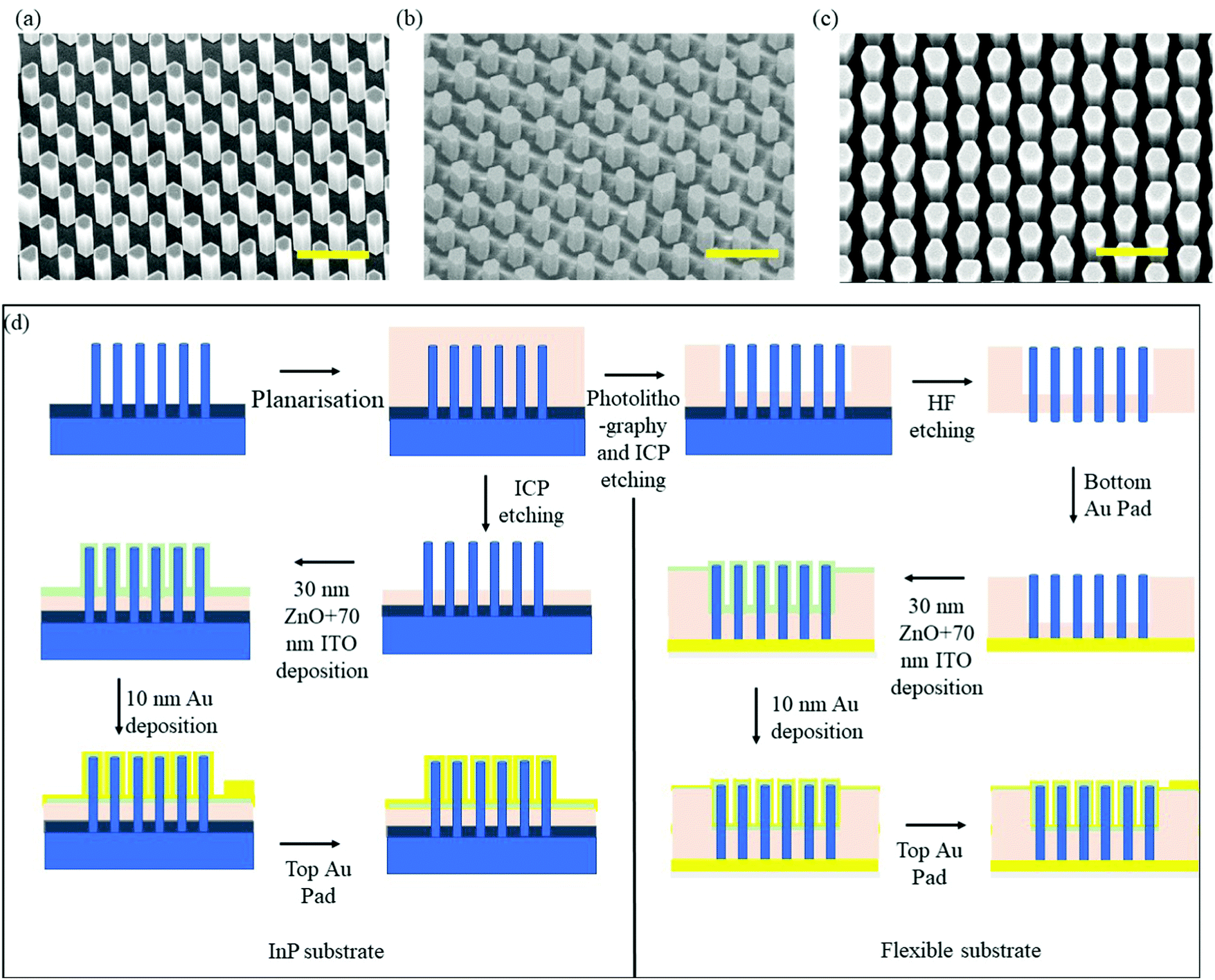 | ||
| Fig. 1 SEM images of the InP NW array after growth and during the LED fabrication process at a 15° tilted view. (a) As-grown NW array. (b) After SU-8 etching with ICP-RIE. (c) After ZnO, ITO and Au deposition. All scale bars are 2 μm. (d) Schematic diagram of the LED fabrication process of the (left) on-substrate and (right) flexible device. | ||
Fig. 1(d) shows a schematic of the fabrication process. After growth, the entire NW array was planarised using SU-8, a transparent electrically insulating polymer by spin coating at 3000 rpm and baking at 95 °C for 2 min, which resulted in a thickness of 5 μm. To expose the top of the wires, inductively coupled plasma reactive ion etching (ICP-RIE) was carried out. SF6/O2/Ar gas chemistry was used with a flow rate of 2/10/20 sccm and a pressure of 1.33 hPa with ICP and bias powers of 300 and 20 W, respectively. Fig. 1(b) shows the SEM image after etching. The top of the NWs was exposed to a depth of ∼2 μm. A 30 nm-thick conformal n-ZnO layer was then deposited using ALD at 150 °C. Finally, 70 nm ITO and 10 nm Au layers were deposited using sputter deposition to decrease the contact resistance (Fig. 1(c)), followed by 150 nm of Au pad deposition using an electron beam evaporator adjacent to the NW array using a shadow mask. To make the bottom contact, the InGa alloy was applied on the back of the p-type wafer.
To prepare flexible LEDs, after planarisation, UV exposure for 1 min and hard baking at 150 °C for 5 min were subsequently performed to enhance the cross-linking of SU-8 to make it mechanically, chemically and thermally strong. After this, photolithography using the MaN-1420 resist was performed to expose only the top of the NWs for subsequent ICP etching under the same conditions as mentioned above. Then, the sample was dipped into 48% hydrofluoric acid for 5 min to etch off the SiO2 mask layer and lift off the NWs embedded inside the SU-8 film. The sample was flipped and a 150 nm Au layer was deposited as the back contact using an electron beam evaporator. This thin film was then transferred onto a transparent acetate film pre-deposited with Au pads. To bond the back contact of the NW array with the Au pads on the transparent film, silver paste was applied. Then, an n-ZnO film with a thickness of ∼30 nm was deposited using atomic layer deposition to form the radial heterojunction, followed by 70 nm ITO and 10 nm Au deposition for the top contact. All the edges of the polymer film were covered with Kapton tape to avoid shorting during ZnO deposition. Finally, a 150 nm top Au pad was made near the NW array using a shadow mask (Fig. S1, ESI†).
To characterise the electrical and optical properties, both electroluminescence (EL) and photoluminescence (PL) measurements were performed using a home-built μ-PL system using a CCD (Princeton Instruments, PIXIS)) and a spectrometer (Acton, SpectraPro 2750). I–V measurements were carried out using a Keysight B2902A source/measurement unit.
To understand the junction properties, electron beam induced current (EBIC) measurements were performed on the on-substrate device using an FEI Helios 600 Nanolab FIB system with a beam current of 0.17 nA and an accelerating voltage of 2 kV. For this purpose, after SAE growth, a 120 nm ZnO layer was deposited using similar conditions on NWs with a diameter of ∼500 nm. ICP-RIE etching was performed to expose the top of the NWs so that the cross-section could be clearly seen under the microscope. Finally, a thin layer of SU-8 was spin-coated to avoid shorting and ICP etching was performed to expose the tips of the embedded NWs. To measure the signals from the NWs, the substrate and thus the NW core were electrically contacted with the FIB stage and the ZnO shell was contacted using a nano-manipulator inside the FIB chamber.
Results and discussion
First, we measured the I–V characteristics of heterojunction ZnO–InP NW LEDs fabricated on the InP substrate. Fig. 2(a) shows a rectifying behaviour typical of an LED with a turn-on voltage of around 4 V and a series resistance of around 88.9 Ω (Fig. S2(a), ESI†). To have a deeper understanding of the I–V characteristics, the ln(I) vs. V plot was constructed, the slope of which gives an ideality factor (n) of 12.2 and the y intercept gives a reverse saturation current of 24.6 nA (Supplementary 1 and Fig. S2(b), ESI†). Here, an ideality factor larger than 2 is consistent with previously reported InP NW LEDs and implies that the current is dominated by tunnelling.19,26 Another reason for the high ideality factor may be the formation of a native oxide layer at the InP/ZnO interface.39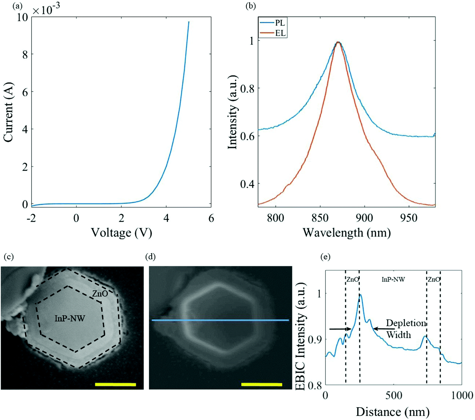 | ||
| Fig. 2 (a) I–V characteristics of the on-substrate device at room temperature. (b) PL spectrum at a 17 μW excitation power and EL spectrum at a 5 mA current. (c) SEM image of a single NW from the fabricated LED array. The image on the top left corner is the contact probe in good contact with the ZnO shell. (d) EBIC signal acquired under an accelerating voltage of 10 kV corresponding to the SEM image in (c). (e) EBIC scan profile across the NW, indicated by the blue solid line. Scale bars in (c) and (d) are 300 nm. | ||
The room temperature EL spectrum measured at 5 mA is shown in Fig. 2(b), in comparison with their PL spectrum. Both spectra display a same peak at 870 nm confirming that Joule heating is kept to a minimum in our device even at continuous current injection. In the PL spectrum, the appearance of only one peak at 870 nm confirms that NWs have a pure WZ structure. It has previously been reported that, for the above-mentioned growth conditions, the NWs have a pure WZ phase irrespective of Zn doping concentration.40 However, in the EL spectrum, a shoulder at a higher wavelength is observed which will be discussed later.
The property of the p-InP/n-ZnO heterojunction was investigated using the EBIC measurement of an individual NW device. Fig. 2(c) shows the cross-sectional SEM image of the NW, with a clearly visible contrast of the InP NW core and ZnO shell. Fig. 2(d) displays the corresponding EBIC signal measured under an accelerating voltage of 2 kV and a 0.17 nA current. From Fig. 2(d), a bright ring can be observed at the NW–ZnO interface, which can be attributed to the depletion region where the highest EBIC current is produced under 0 V bias. The EBIC intensity profile is plotted across the diameter of the NW as shown in Fig. 2(e). The depletion width is approximately 138 nm when measured at 1/e of the maximum intensity value. Using the depletion width we estimated the p-doping level in the NW to be 6.75 × 1016 cm−3 which is consistent with previously reported values (Supplementary 3, ESI†).40 To calculate the carrier concentration of ZnO (ND), a planar 30 nm film of n-ZnO deposited under the same conditions on a glass substrate was calculated to be 2 × 1019 cm−3 using a combination of Drude and Cody–Lorentz models by ellipsometry and is consistent with the reported values in the literature.41 It is noticed that the EBIC profile is asymmetric, extending more into p-doped NWs. This confirms that the depletion region is primarily formed in the NW where the majority of recombination occurs in this region. The possible reason for the non-symmetric profile at both the junctions could be a small angle tilt or non-uniform ICP etching of the ZnO shell which is evident from the SEM image (Fig. 2(c)).
Fig. 3(a) shows the EL spectra from the NW array LEDs on the substrate with increasing forward current injection level at room temperature. The EL signal is detectable at an injection current of 1 mA, showing a peak at 870 nm with a shoulder at around 920 nm. To investigate the origin of different peaks, Lorentz curve fitting was performed (Fig. 3(e)). It is found that there are three peaks with a major contribution from the peak at 1.42 eV which corresponds to the fundamental bandgap of WZ InP NWs.42,43 The peak at a higher energy of 1.46 eV is due to the light hole and heavy hole splitting in WZ structures.44 A. Zilli et al. reported that this peak becomes dominant at temperatures above 150 K due to thermal population of higher energy states.42 The energy difference between these two peaks has been reported to be around 40 meV, consistent with our value of 37.8 meV.42,44,45 We attributed the peak at the lowest energy of 1.34 eV to the recombination occurring at the ZB InP substrate.43 The existence of this peak confirms that some carriers leak into the substrate from NWs. With the increase of injection current, the EL intensity increases with the peak position slightly red-shifted to longer wavelengths due to Joule heating. Fig. 3(b) shows the optical microscopy image of the NW LED array captured using an infrared camera with a 10× lens. It is clearly evident that light is emitted from the NWs, and with the increase of current injection, the emission intensity becomes more uniform across the entire array.
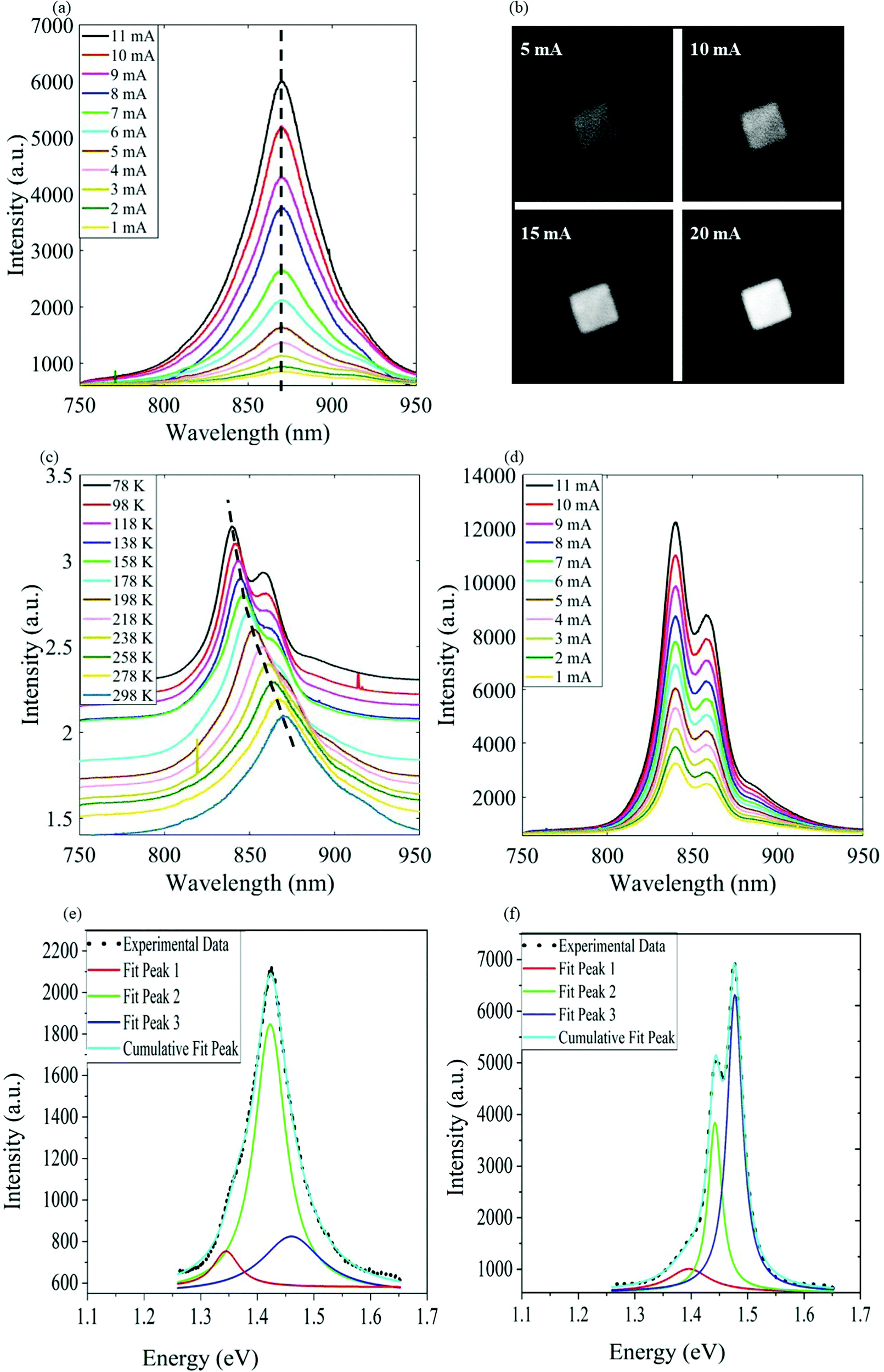 | ||
| Fig. 3 On-substrate NW array LED characteristics of the device. (a) Room temperature EL spectrum at different current injection levels. The black dashed line indicates the peak of the spectrum at 870 nm. (b) Optical images of the emission at room temperature from the 100 × 100 μm2 array at different current injection levels. (c) Temperature dependent EL spectrum of the device at a 5 mA current where the black dashed line indicates the peak position. (d) EL spectrum at 78 K at different current injection levels. Lorentz curve fitting of the EL spectrum measured at 5 mA at (e) room temperature and (f) 78 K. | ||
To investigate the temperature dependent characteristics of the device, EL was conducted at an injection current of 5 mA from room temperature to 78 K and the spectrum is shown in Fig. 3(c). The linewidth decreases with decreasing temperature and the spectrum is blue-shifted as a result of increased bandgap with the decrease of temperature.42 Interestingly, at ∼238 K, we observed another peak in the EL spectrum, which becomes more prominent at lower temperatures. Fig. 3(d) indicates the LED behaviour at 78 K as a function of increasing injection current. To understand the origin of this peak, Lorentz fitting was performed at 78 K (Fig. 3(f)) and 3 peaks were observed. The highest energy peak at 1.48 eV corresponds to the bandgap of NWs which is also known as the A exciton peak in the WZ semiconductor. We attribute the lower energy peak at 1.44 eV to radiative recombination from the conduction band to the Zn acceptor in the NWs. We calculated the activation energy of the Zn acceptor level for a doping concentration of 6.75 × 1016 cm−3 obtained from EBIC measurements using the formula given by K. Hansen et al.46
| EA = E0 − a(NA−)1/3 | (1) |
The comparison between the I–V characteristics of the flexible device and on-substrate device in Fig. 4(a) shows that the turn-on voltages for both devices are similar at ∼3.5 V using an extrapolation method described in the Section S5 (ESI†). However, there is a ‘softer’ turn-on voltage for the flexible device. The flexible LED is also slightly more resistive compared to the on-substrate one, which might be due to the poorer contact formed on the flexible device using silver adhesive paste.
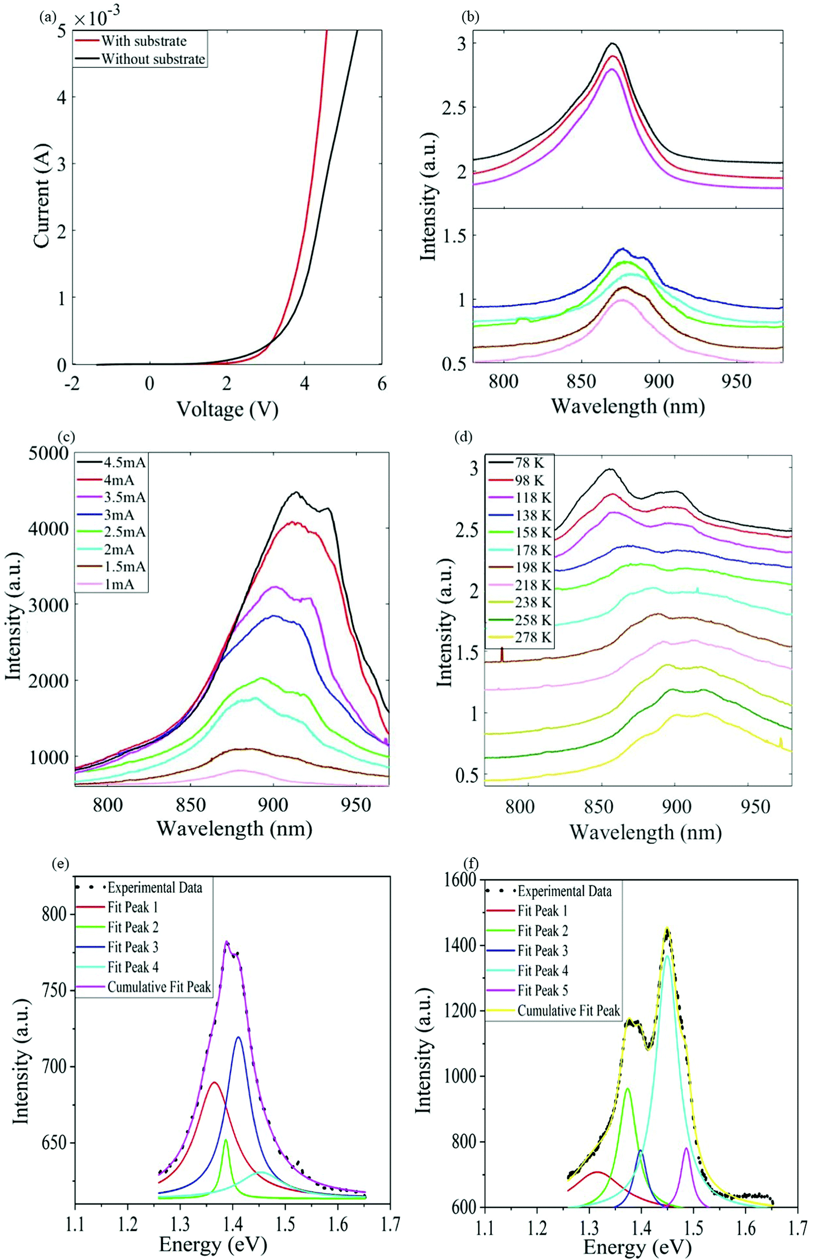 | ||
| Fig. 4 (a) I–V characteristics of the on-substrate and flexible devices. (b) Room temperature PL spectrum at different positions on the array for on-substrate (top) and flexible devices (bottom). (c) EL spectrum of the flexible device at room temperature at different current injection levels. (d) Temperature dependent EL spectrum at a 1 mA current from the flexible LED. Lorentz curve fitting of the EL spectrum measured at 1 mA at (e) room temperature and (f) 78 K. | ||
To compare with the on-substrate NW LEDs, the PL characteristics of flexible LEDs were investigated. As shown in Fig. 4(b), multiple, red-shifted and broader PL peaks were observed from the flexible device, in comparison to the on-substrate device. Furthermore, the peak of the PL spectrum varies across the array, which is not observed for the on-substrate device. A possible explanation for these multiple peaks could be the effect of non-uniform strain on the NW array imposed by the SU-8 film or the acetate film.50–52 We mapped the surface profile of the peeled SU-8 film after integration on the acetate sheet using an optical profilometer (Fig. S3, ESI†) and observed that one radius of curvature varies across the NW array. However, due to measurement setup limitations, we could not quantify the strain induced in the NW array. Moreover, the intensity of the emission decreases significantly in comparison to the on-substrate device due to the wavy nature of the flexible device which leads to less light entrance into the detector.
Fig. 4(c) shows that, as the injection current increases, there is a significant red shift in the EL spectrum due to Joule heating. In comparison, the on-substrate device does not show any significant shift in the emission wavelength (Fig. 3(a)). This effect can be understood in terms of the InP substrate providing better heat dissipation in comparison to the transparent acetate film used for supporting the flexible device. We also fit the EL spectrum obtained at 1 mA and found that two additional peaks at longer wavelengths (peak 1 and peak 2) in addition to the fundamental bandgap peak (peak 3) and transition from the conduction band to the light hole band (peak 4) (Fig. 4(e)). The recombination from the conduction band to the heavy hole band and the light hole band is observed at 1.41 eV and 1.45 eV, respectively. Red shift from the actual position is due to heating; however, the energy difference remains around 40 meV. The possible reason for the two additional red-shifted peaks might be strain related. Since the radius of curvature varies across the NW array, it may induce non-uniform strain at different positions, similar to the report by G. Signorello et al.51
The temperature dependent behaviour of these peaks was further studied by measuring the EL spectra at an injection current of 2 mA from room temperature to 78 K. As shown in Fig. 4(d), the emission spectrum is blue-shifted with decreasing temperature due to the temperature dependence of bandgap. Moreover, slightly red-shifted, broader and multiple peaks are observed (Fig. 4(f)) as compared to the on-substrate device which is possibly due to the combined effect of heating and strain induced by the SU-8 and/or acetate film on the NWs due to thermal coefficient mismatch.50–52 Moreover, a small peak at a higher energy with a difference of ∼40 meV indicates the splitting of heavy hole and light hole bands confirming that the temperature is higher than 150 K as this peak becomes dominant at temperature above 150 K due to thermal population of higher energy states.42
Conclusions
In summary, we have demonstrated core–shell InP/ZnO heterojunction NW LED arrays and successfully fabricated flexible LEDs by embedding the NWs in a thin SU-8 film, which is then peeled off from the InP substrate. We have also studied the temperature dependent behaviour of these LEDs and confirmed that the EL spectrum consists of 3 peaks at both room temperature and 78 K. The peaks related to conduction band-to-heavy hole band transition and recombination at the substrate are present across the temperature range, whereas the peak related to the transition from the conduction band to the light hole band quenches at a low temperature and the Zn acceptor level peak became prominent at around 238 K. Our work provides a pathway for integrating LEDs on various substrates irrespective of their shapes, lattice constants, and chemical and mechanical properties. Future work will be carried out to further optimise the fabrication process and improve heat sinking (to minimise Joule heating) to enhance the performance of the flexible device for a plethora of applications as low power and portable light sources.Conflicts of interest
The authors declare no conflicts of interest.Acknowledgements
We acknowledge the Australian Research Council for financial support and the Australian National Fabrication Facility (ANFF ACT node) for providing access to the epitaxial growth and device fabrication tools used in this work. We also thank the ANFF staff for their guidance.References
- H. Sasabe and J. Kido, J. Mater. Chem. C, 2013, 1, 1699–1707 RSC.
- W. Brütting, J. Frischeisen, T. D. Schmidt, B. J. Scholz and C. Mayr, Phys. Status Solidi A, 2013, 210, 44–65 CrossRef.
- T. Sekitani, H. Nakajima, H. Maeda, T. Fukushima, T. Aida, K. Hata and T. Someya, Nat. Mater., 2009, 8, 494–499 CrossRef CAS PubMed.
- N. Thejokalyani and S. J. Dhoble, Renewable Sustainable Energy Rev., 2014, 32, 448–467 CrossRef CAS.
- D. A. Gaul and W. S. Rees Jr., Adv. Mater., 2000, 12, 935–946 CrossRef CAS.
- F. A. Ponce and D. P. Bour, Nature, 1997, 386, 351–359 CrossRef CAS.
- H. Aziz, Z. D. Popovic, N. X. Hu, A. M. Hor and G. Xu, Science, 1999, 283, 1900–1902 CrossRef CAS PubMed.
- L. Han, M. Zhao, X. Tang, W. Huo, Z. Deng, Y. Jiang, W. Wang, H. Chen, C. Du and H. Jia, J. Appl. Phys., 2020, 127, 085706 CrossRef CAS.
- C. Huh, K.-S. Lee, E.-J. Kang and S.-J. Park, J. Appl. Phys., 2003, 93, 9383–9385 CrossRef CAS.
- T. Nishida, H. Saito and N. Kobayashi, Appl. Phys. Lett., 2001, 79, 711–712 CrossRef CAS.
- W. H. Haydl, H. D. Müller, H. Ennen, W. Körber and K. W. Benz, Appl. Phys. Lett., 1985, 46, 870–872 CrossRef CAS.
- S. X. Jin, J. Li, J. Z. Li, J. Y. Lin and H. X. Jiang, Appl. Phys. Lett., 2000, 76, 631–633 CrossRef CAS.
- S. X. Jin, J. Li, J. Y. Lin and H. X. Jiang, Appl. Phys. Lett., 2000, 77, 3236–3238 CrossRef CAS.
- L. Dai, B. Zhang, J. Y. Lin and H. X. Jiang, J. Appl. Phys., 2001, 89, 4951–4954 CrossRef CAS.
- E. D. Minot, F. Kelkensberg, M. van Kouwen, J. A. van Dam, L. P. Kouwenhoven, V. Zwiller, M. T. Borgström, O. Wunnicke, M. A. Verheijen and E. P. A. M. Bakkers, Nano Lett., 2007, 7, 367–371 CrossRef CAS PubMed.
- X. Dai, A. Messanvi, H. Zhang, C. Durand, J. Eymery, C. Bougerol, F. H. Julien and M. Tchernycheva, Nano Lett., 2015, 15, 6958–6964 CrossRef PubMed.
- V. Neplokh, A. Messanvi, H. Zhang, F. H. Julien, A. Babichev, J. Eymery, C. Durand and M. Tchernycheva, Nanoscale Res. Lett., 2015, 10, 447 CrossRef PubMed.
- J. Garra, T. Long, J. Currie, T. Schneider, R. White and M. Paranjape, J. Vac. Sci. Technol., A, 2002, 20, 975–982 CrossRef CAS.
- S. Maeda, K. Tomioka, S. Hara and J. Motohisa, Jpn. J. Appl. Phys., 2012, 51, 02BN03 CrossRef.
- J. Wallentin, N. Anttu, D. Asoli, M. Huffman, I. Åberg, M. H. Magnusson, G. Siefer, P. Fuss-Kailuweit, F. Dimroth, B. Witzigmann, H. Q. Xu, L. Samuelson, K. Deppert and M. T. Borgström, Science, 2013, 339, 1057–1060 CrossRef CAS PubMed.
- Q. Gao, D. Saxena, F. Wang, L. Fu, S. Mokkapati, Y. Guo, L. Li, J. Wong-Leung, P. Caroff, H. H. Tan and C. Jagadish, Nano Lett., 2014, 14, 5206–5211 CrossRef CAS PubMed.
- X. Duan, Y. Huang, Y. Cui, J. Wang and C. M. Lieber, Nature, 2001, 409, 66–69 CrossRef CAS PubMed.
- K. Peng, P. Parkinson, Q. Gao, J. L. Boland, Z. Li, F. Wang, S. Mokkapati, L. Fu, M. B. Johnston, H. H. Tan and C. Jagadish, Nanotechnology, 2017, 28, 125202 CrossRef PubMed.
- H. J. Joyce, J. Wong-Leung, C.-K. Yong, C. J. Docherty, S. Paiman, Q. Gao, H. H. Tan, C. Jagadish, J. Lloyd-Hughes, L. M. Herz and M. B. Johnston, Nano Lett., 2012, 12, 5325–5330 CrossRef CAS PubMed.
- M. T. Borgström, E. Norberg, P. Wickert, H. A. Nilsson, J. Trägårdh, K. A. Dick, G. Statkute, P. Ramvall, K. Deppert and L. Samuelson, Nanotechnology, 2008, 19, 445602 CrossRef PubMed.
- J. Motohisa, H. Kameda, M. Sasaki and K. Tomioka, Nanotechnology, 2019, 30, 134002 CrossRef CAS PubMed.
- S. Deshpande, I. Bhattacharya, G. Malheiros-Silveira, K. W. Ng, F. Schuster, W. Mantei, K. Cook and C. Chang-Hasnain, ACS Photonics, 2017, 4, 695–702 CrossRef CAS.
- M. Takiguchi, G. Zhang, S. Sasaki, K. Nozaki, E. Chen, K. Tateno, T. Tawara, A. Shinya, H. Gotoh and M. Notomi, Appl. Phys. Lett., 2018, 112, 251106 CrossRef.
- T. Akamatsu, K. Tomioka and J. Motohisa, Nanotechnology, 2020, 31, 394003 CrossRef CAS PubMed.
- I. Yang, Z. Li, J. Wong-Leung, Y. Zhu, Z. Li, N. Gagrani, L. Li, M. N. Lockrey, H. Nguyen, Y. Lu, H. H. Tan, C. Jagadish and L. Fu, Nano Lett., 2019, 19, 3821–3829 CrossRef CAS PubMed.
- I. Yang, S. Kim, M. Niihori, A. Alabadla, Z. Li, L. Li, M. N. Lockrey, D.-Y. Choi, I. Aharonovich, J. Wong-Leung, H. H. Tan, C. Jagadish and L. Fu, Nano Energy, 2020, 71, 104576 CrossRef CAS.
- I. Yang, X. Zhang, C. Zheng, Q. Gao, Z. Li, L. Li, M. N. Lockrey, H. Nguyen, P. Caroff, J. Etheridge, H. H. Tan, C. Jagadish, J. Wong-Leung and L. Fu, ACS Nano, 2018, 12, 10374–10382 CrossRef CAS PubMed.
- T. C. Shen, G. B. Gao and H. Morkoç, J. Vac. Sci. Technol., B: Microelectron. Nanometer Struct. – Process., Meas., Phenom., 1992, 10, 2113–2132 CrossRef CAS.
- H. Burkhard, H. W. Dinges and E. Kuphal, J. Appl. Phys., 1982, 53, 655–662 CrossRef CAS.
- O. Semyonov, A. Subashiev, Z. Chen and S. Luryi, J. Appl. Phys., 2010, 108, 013101 CrossRef.
- T. Minami, Semicond. Sci. Technol., 2005, 20, S35–S44 CrossRef CAS.
- C. G. Van de Walle, Phys. Rev. Lett., 2000, 85, 1012–1015 CrossRef CAS PubMed.
- E. Guziewicz, T. A. Krajewski, E. Przezdziecka, K. P. Korona, N. Czechowski, L. Klopotowski and P. Terziyska, Phys. Status Solidi B, 2020, 257, 1900472 CrossRef CAS.
- V. Raj, T. S. dos Santos, F. Rougieux, K. Vora, M. Lysevych, L. Fu, S. Mokkapati, H. H. Tan and C. Jagadish, J. Phys. D: Appl. Phys., 2018, 51, 395301 CrossRef.
- Q. Gao, Z. Li, L. Li, K. Vora, Z. Li, A. Alabadla, F. Wang, Y. Guo, K. Peng, Y. C. Wenas, S. Mokkapati, F. Karouta, H. H. Tan, C. Jagadish and L. Fu, Prog. Photovoltaics Res. Appl., 2019, 27, 237–244 CrossRef CAS.
- E. Guziewicz, M. Godlewski, T. Krajewski, Ł. Wachnicki, A. Szczepanik, K. Kopalko, A. Wójcik-Głodowska, E. Przeździecka, W. Paszkowicz, E. Łusakowska, P. Kruszewski, N. Huby, G. Tallarida and S. Ferrari, J. Appl. Phys., 2009, 105, 122413 CrossRef.
- A. Zilli, M. De Luca, D. Tedeschi, H. A. Fonseka, A. Miriametro, H. H. Tan, C. Jagadish, M. Capizzi and A. Polimeni, ACS Nano, 2015, 9, 4277–4287 CrossRef CAS PubMed.
- C. K. Yong, J. Wong-Leung, H. J. Joyce, J. Lloyd-Hughes, Q. Gao, H. H. Tan, C. Jagadish, M. B. Johnston and L. M. Herz, Nano Lett., 2013, 13, 4280–4287 CrossRef CAS PubMed.
- S. Perera, K. Pemasiri, M. A. Fickenscher, H. E. Jackson, L. M. Smith, J. Yarrison-Rice, S. Paiman, Q. Gao, H. H. Tan and C. Jagadish, Appl. Phys. Lett., 2010, 97, 023106 CrossRef.
- G. L. Tuin, M. T. Borgström, J. Trägårdh, M. Ek, L. R. Wallenberg, L. Samuelson and M.-E. Pistol, Nano Res., 2011, 4, 159–163 CrossRef CAS.
- K. Hansen, E. Peiner, A. Schlachetzki and M. Von Ortenberg, J. Electron. Mater., 1994, 23, 935–941 CrossRef CAS.
- K. Li, H. Sun, F. Ren, K. W. Ng, T.-T. D. Tran, R. Chen and C. J. Chang-Hasnain, Nano Lett., 2014, 14, 183–190 CrossRef CAS PubMed.
- T. T. T. Vu, T. Zehender, M. A. Verheijen, S. R. Plissard, G. W. G. Immink, J. E. M. Haverkort and E. P. A. M. Bakkers, Nanotechnology, 2013, 24, 115705 CrossRef PubMed.
- M. De Luca, A. Polimeni, H. A. Fonseka, A. J. Meaney, P. C. M. Christianen, J. C. Maan, S. Paiman, H. H. Tan, F. Mura, C. Jagadish and M. Capizzi, Nano Lett., 2014, 14, 4250–4256 CrossRef CAS PubMed.
- J. C. González, M. I. N. da Silva, X. S. Lozano, D. Zanchet, D. Ugarte, E. Ribeiro, H. R. Gutiérrez and M. A. Cotta, J. Nanosci. Nanotechnol., 2006, 6, 2182–2186 CrossRef PubMed.
- G. Signorello, S. Karg, M. T. Björk, B. Gotsmann and H. Riel, Nano Lett., 2013, 13, 917–924 CrossRef CAS PubMed.
- R. Anufriev, N. Chauvin, H. Khmissi, K. Naji, M. Gendry and C. Bru-Chevallier, Appl. Phys. Lett., 2012, 101, 072101 CrossRef.
Footnote |
| † Electronic supplementary information (ESI) available. See DOI: 10.1039/d1nh00535a |
| This journal is © The Royal Society of Chemistry 2022 |