
 Open Access Article
 This Open Access Article is licensed under a Creative Commons Attribution-Non Commercial 3.0 Unported Licence
Direct 3D-printed CdSe quantum dots via scanning micropipette†
Taesun
Yun
a,
Yong Bin
Kim
a,
Taegeon
Lee
a,
Heesuk
Rho
a,
Hyeongwoo
Lee
b,
Kyoung-Duck
Park
b,
Hong Seok
Lee
 *a and
Sangmin
An
*a
*a and
Sangmin
An
*a
aDepartment of Physics, Research Institute of Physics and Chemistry, Jeonbuk National University, Jeonju 54896, Republic of Korea. E-mail: hslee1@jbnu.ac.kr; san@jbnu.ac.kr
bDepartment of Physics, Pohang University of Science and Technology (POSTECH), Pohang 37673, Republic of Korea
First published on 28th November 2022
Abstract
The micropipette, pencil-shaped with an aperture diameter of a few micrometers, is a potentially promising tool for the three-dimensional (3D) printing of individual microstructures based on its capability to deliver low volumes of nanomaterial solution on a desired spot resulting in micro/nanoscale patterning. Here, we demonstrate a direct 3D printing technique in which a micropipette with a cadmium selenide (CdSe) quantum dot (QD) solution is guided by an atomic force microscope with no electric field and no piezo-pumping schemes. We define the printed CdSe QD wires, which are a composite material with a QD–liquid coexistence phase, by using photoluminescence and Raman spectroscopy to analyze their intrinsic properties and additionally demonstrate a means of directional falling.
Introduction
Three-dimensional (3D) printing plays an important role for convergence techniques in various research and industrial fields based on its powerful application capability.1–3 One of the fundamental objects for 3D printing fabrication can be said to be one-dimensional (1D) wires,4,5 for which there is an expectation that reducing the diameters of the fabricated 1D wires down to the nanoscale will increase 3D printing applications with high resolution. For the fabrication of 1D nanoscale wires with various material solutions, several techniques have been introduced including electrospray,6–8 carbon nanotube catalyst,9,10 e-beam base printing,11,12 and so on. Among such developments, one of the most advanced technologies is dip-pen lithography using a nanopipette as a single pen, which has advantages of low energy consumption and a relatively short fabrication time.13–15 This innovative development has made a great contribution to the fabrication of molecules for desired purposes such as circuit design and molecular alignment. Another potential tool for lithography or 3D fabrication is the pencil-shaped micropipette, which is a single pen mainly used to inject substances such as solvents into cells in biological fields.16 But in contrast to the soft surfaces of cells and other biomaterials, hard surfaces pose a potential problem of the breaking of the pipette tip upon direct contact with a hard surface. Recently, nanopipette/quartz tuning fork-based atomic force microscope (QTF-AFM) fabrication techniques have been reported that are able to produce ∼100 nm diameter Au-aggregated nanowires by applying an electric field between the inside of the nanopipette and the substrate in the presence of a nanoscale water meniscus formed between the tip apex rim and the substrate.17,18 However, this method requires an electric field application system along with additional electrodes for biasing both the inside of the pipette and the substrate.Here, we introduce a micropipette with an outer diameter of about 1 μm that employs QTF-AFM guidance19–21 to eject a small amount of liquid containing nanomaterials such as cadmium selenide (CdSe) quantum dots (QDs) onto a glass substrate (Pyrex glass, 2 cm × 2 cm × 250 μm) with no requirement for electric field application or additional electrodes. The fabrication procedure is simple and clear with the following steps: (i) filling liquid solution inside the micropipette without any treatment, (ii) approaching the substrate without an additional electric field and ejecting the liquid without breaking the pipette tip via AFM guidance, and (iii) retracting the tip from the substrate, thereby forming micro/nanoscale wires with diameters that match the aperture diameter of the micropipette.
Methods
The basic operation method of a non-contact AFM is that a micropipette-attached QTF moves on the surface and reads the amplitude and phase variation from the force of the liquid bridge formed between the liquid inside of the pipette and the substrate.22,23 We adopted the QTF-AFM system for the high stiffness of the oscillator that allows true non-contact operation without damaging the pipette tip and has a high-quality factor on the order of about a few thousand compared to conventional cantilevers (<100 N m−1). For the fabrication of micro/nanoscale wires, liquid ejection is followed by a retraction of the pipette from the substrate, which forms the wire at the point that the oscillation amplitude of the tip rapidly decreases, i.e., the formation spot of the liquid bridge.After fabrication, we demonstrate a directional falling of the printed CdSe QD wires followed by photoluminescence (PL) analysis to confirm the 3D printed wires and Raman spectroscopy to obtain the molecular information. By analyzing particular atomic vibrations originating from inelastic light scattering from a crystal by laser irradiation, Raman spectroscopy provides unique optical phonon characteristics that can be used to identify the atomic components and crystalline quality of the investigated sample. In the present case, Raman mapping is a particularly effective technique for locating the spatial distributions of the QDs that are embedded along the nanowire long axis during the 3D printing process.
Results and discussion
Fig. 1 shows the experimental setup of the proposed micropipette-combined QTF-AFM. The basic schematic in Fig. 1a illustrates that the pulled micropipette, with an outer diameter of the tip of about 1 μm, is attached to one prong of the QTF resonator. The CdSe QD filled micropipette approaches a glass surface with the guidance of the QTF system, forms liquid bridge between the tip and the substrate, and finally retracts for the formation of CdSe QD wires as a 3D printing scheme. Fig. 1b is a photograph of the experimental setup showing the glass substrate, tip, and objective lens under the area of interest to monitor the behavior of the approaching pipette tip. Fig. 1c shows the overall design of the micropipette-combined AFM setup. Three charge-coupled device (CCD) cameras are installed in this setup for monitoring the x-, y-, z-axes for tip breakage and reducing the tip approach time. Among them, the camera installed along the z-axis views the sample from below for a clear observation of the tip apex, focusing on the glass surface where the fabrication is in progress. Although we can observe the surface and pipette tip clearly with the z-axis camera, the approach to the surface should be precisely guided by the AFM to avoid breaking the tip. The x, y, z positions of the system can be controlled in detail using a piezo linear actuator (Picomotor™, Newport Co.) controller, and the tip can be positioned as close as possible to the surface with a z-axis motor controller prior to fabrication.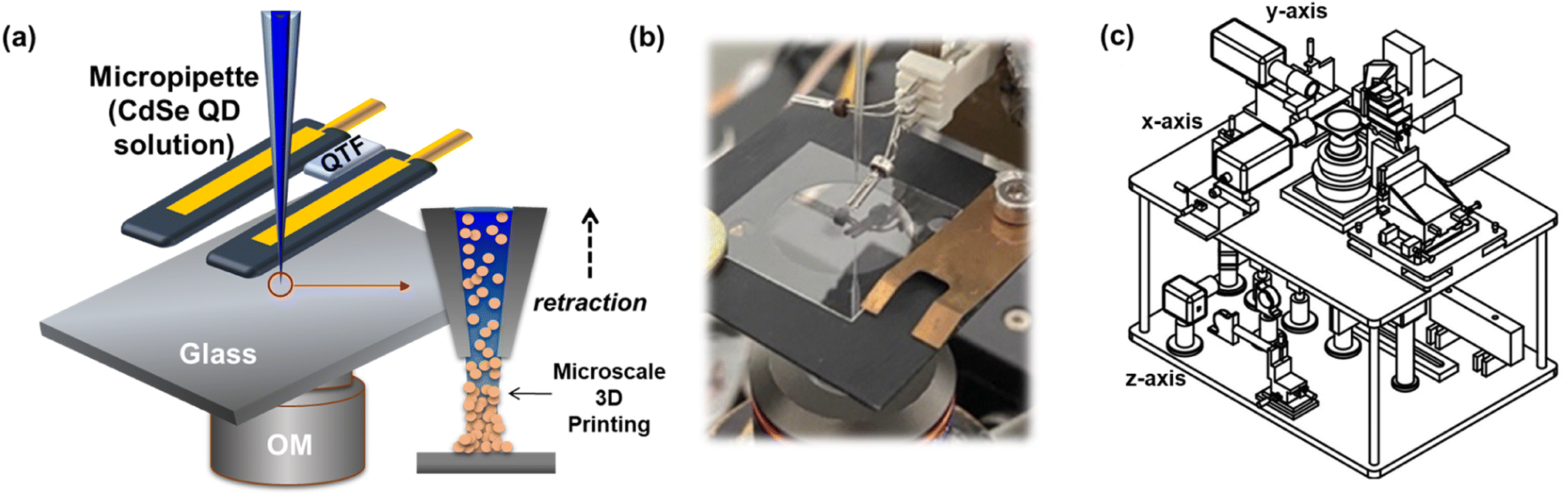 | ||
| Fig. 1 Micropipette-combined QTF-AFM system. (a) Schematic of the experimental setup for the fabrication of QD-aggregated wires. (b) Photograph of the experimental setup. (c) Schematic of the CCD cameras on the x-, y-, z-axes that monitor each phenomenon. Through these cameras, it is possible to know where the micropipette tip is located on the surface of the sample. | ||
We fabricate the micropipette for the experiments using a mechanical puller (PC-100, Narishige Co.) (Fig. 2). Fig. 2a shows a schematic of the pulling operation. A borosilicate pipette with an outer diameter of 1 mm and inner diameter of 0.5 mm is clamped to the puller on each end and then melted with a coil heater while gravity pulls the pipette down, which creates the pencil-shaped pipette to be used in the experiment. Pulled pipettes with desired shapes and diameters can be made in this way by adjusting the melting temperature and the attached mass of the puller. In terms of the melting temperature, different shapes (e.g., tapered angles) can be obtained by melting the pipette at different temperature values, and different diameters of the pipette apex can be obtained by immediately melting the pipette.
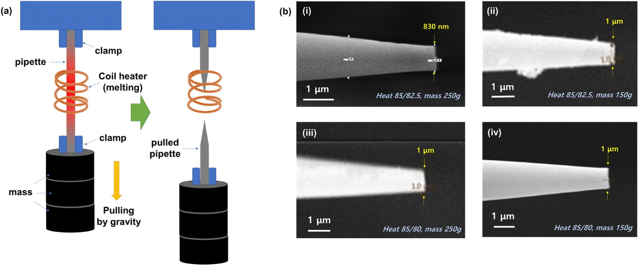 | ||
| Fig. 2 Fabrication of the experimental micropipette. (a) Schematic of the mechanical puller setup. After clamping, the borosilicate pipette is pulled by gravity while the middle area is melted with a coil heater. (b) Scanning electron microscope images of pencil-shaped pipettes with varying pulling parameters of heat and mass in four conditions showing a similar edge outer diameter of ∼1 μm, indicating an aperture diameter of ∼500 nm. | ||
We varied the control parameters in terms of the heating value (heat ##, where the number indicates the intensity value, not temperature) and the mass in four different conditions as shown in Fig. 2b: (i) heat 85(Step 1)/82.5(Step 2), mass 250 g; (ii) heat 85(Step 1)/82.5(Step 2), mass 150 g; (iii) heat 85(Step 1)/80(Step 2), mass 250 g; (iv) heat 85(Step 1)/80(Step 2), mass 150 g. We considered two criteria for selecting a pulled pipette for further use. The first is an apex diameter similar to the original pipette apex outer diameter of ∼1 μm, which indicates an aperture diameter of ∼500 nm (corresponding to the diameter of the fabricated CdSe QD wires) based on maintaining the same ratio of the initial bare pipette (outer diameter 1 mm, inner diameter 0.5 mm). The second is the shape of the pipette. The reason why the tip shape of the pipette is important is that when the tip is attached to one prong of the QTF, the quality factor is influenced by the tip shape, where a tapered angle in the shape of pencil can capture a high Q-factor.16 Among the four tested conditions, we decided to use pulled pipettes following the third and fourth conditions (Fig. 2b-(iii) and (iv)) for the experiments.
After selecting the pulled pipette to be used in the experiment, we filled it with CdSe QD solution (Fig. 3). Fig. 3a shows the filling process using the capillary force exerted between the inner wall of the pipette and a pre-bonded filament, where the solution rises to the apex of the pipette due to the surface tension of the liquid.17 Using this phenomenon, we filled the solution to the edge without any air pockets. We then attached the micropipette containing CdSe QD solution to one prong of the QTF sensor to proceed with the 3D printing. To check whether the micropipette is firmly attached or not, we obtained resonance curves of the sensor with and without the attachment of the pulled micropipette to one prong of the QTF sensor. After attachment of the tip, the sensor quality factor and amplitude decreased with a decrement in resonance frequency. Note that if the thickness of the micropipette is too high at the point of attachment to the QTF prong, the quality factor will disappear and the amplitude and phase signals could not be captured (Fig. 3b).
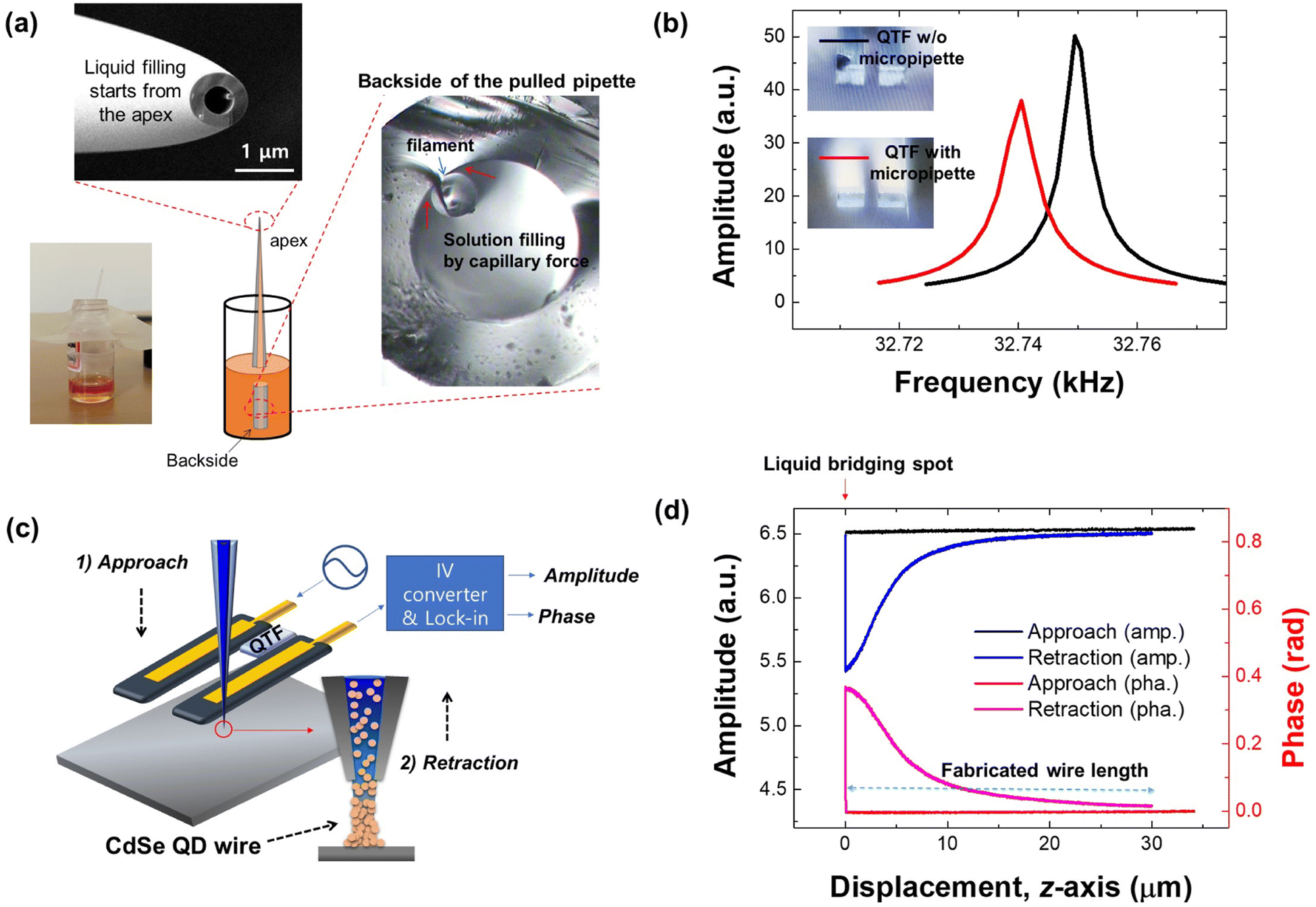 | ||
| Fig. 3 3D printing with a pulled micropipette. (a) Images and schematic of the liquid inside the micropipette. We place the backside of the micropipette into CdSe QD solution to completely fill it up to the apex by capillary force. The SEM image shows an apex outer diameter of ∼1 μm and aperture diameter of ∼500 nm. (b) Resonance curves of the QTF sensor with and without the attachment of the pulled micropipette. Inset: images of the sensor with and without the micropipette. (c) Approach while monitoring the lock-in signals to avoid tip breakage, and retraction to form the CdSe QD wire. (d) Approach/retraction curves of the amplitude and phase signals of the sensor. | ||
Now we bring the pulled micropipette toward the glass surface while monitoring the amplitude variation at a resonance frequency of ∼32.75 kHz (Fig. 3c). We monitored the experiment with a QTF sensor driven with a function generator while obtaining the amplitude and phase responses with a lock-in amplifier. As the tip closely approaches the glass surface, a nanoscale water meniscus is suddenly formed between the rim of the tip apex and the surface. When the pipette tip approaches the surface within a few nanometers, water molecules in the air suddenly forms the nanoscale water meniscus between the hydrophilic tip and the hydrophilic substrate by experience of phase transition from liquid state to liquid state due to lowering energy barrier by reducing distance between the tip and the surface, which is previously researched by quartz tuning fork-atomic force microscope system.22–24 The CdSe QD solution then forms a liquid bridge and starts to eject, which is accompanied by a rapid decrease in the amplitude and phase signals (Fig. 3d). At this point, we retract the micropipette for the formation of a CdSe QD wire, thereby maintaining non-contact operation over the whole process of 3D printing with the pipette.18 The length of the 3D printed CdSe QD wire can be controlled by the point of the retraction. For retraction at a certain point, which corresponds to the length of the CdSe QD wire, we suddenly pull back the tip to break the bridge between the tip apex and the wire. After retraction of the tip, we lay down the fabricated CdSe QD wire via pipette tip control. It is common sense that it is difficult to form a well-defined solid-state wire from the macroscopic liquid meniscus while the liquid evaporates. However, in the case of microscale or nanoscale, the liquid solvent of QD solution evaporates in an instant while the tip retraction through the micro or nanoscale aperture of the pipette. Thus, the well-defined solid-state wire will eventually be left with the aggregated QD particles, allowing the resulting wire to stand upright. 3D printing technology is emerging field, and interest in nanoscale printing is increasing as a high-resolution printing which is one of the important considerable factors. The diameter of the wire produced by this printing technique depends on the size of the inner diameter of the tip of the pipette. Normally, one can fabricate a pencil-shaped pipette by applying heat or laser and pulling a borosilicate or quartz pipette. Using the laser irradiation, the aperture size of pencil-shaped pipette hole can be fabricated about 100 nm which corresponding to fabrication of the particle-aggregated nanowires of about 100 nm.17 In addition, the pipette is precisely approaches to the surface with a guidance of the AFM, the tip can be protected very safely. Since an extremely small amount of QD solution is ejected for fabrication of the microwires or nanowires compared to the filled QD solution amount inside of the pipette, it can be printed repeatedly.
We fabricate CdSe QD wires with a diameter of about 500 nm by using the pulled micropipette-combined AFM system as a nanoscale 3D printing scheme. Fig. 4 shows the fabricated CdSe QD wires (#1–#5) revealed by a scanning electron microscope (SEM). As expected, the diameter of the fabricated wires is about 500 nm, corresponding to the aperture diameter of the pipette. The diameter of the QD wires fabricated in this experiment is ∼500 nm, because the inner diameter of the used pipette at the apex is ∼500 nm. As the material of the micropipette is borosilicate glass with outer diameter (1 mm) and inner diameter (0.5 mm) ratio of 2![[thin space (1/6-em)]](https://www.rsc.org/images/entities/char_2009.gif) :1, inner diameter and outer diameter at the apex shows similar ratio as 1 μm and 500 nm resulting quite reproducible 500 nm QD wires. We assume that the fabricated wires have a QD–liquid coexistence phase, even though the liquid evaporates during retraction.17 For the purpose of demonstrating directional falling, we laid the fabricated CdSe QD wire down on the substrate in three cases by controlling the pipette tip (#1, #2, and #3 in Fig. 4) and kept the wire vertically sustained in two cases (#4 and #5 in Fig. 4). Note that even when vertically sustained, the wire tilted a bit, which we assume resulted from the quick retraction of the pipette tip.
:1, inner diameter and outer diameter at the apex shows similar ratio as 1 μm and 500 nm resulting quite reproducible 500 nm QD wires. We assume that the fabricated wires have a QD–liquid coexistence phase, even though the liquid evaporates during retraction.17 For the purpose of demonstrating directional falling, we laid the fabricated CdSe QD wire down on the substrate in three cases by controlling the pipette tip (#1, #2, and #3 in Fig. 4) and kept the wire vertically sustained in two cases (#4 and #5 in Fig. 4). Note that even when vertically sustained, the wire tilted a bit, which we assume resulted from the quick retraction of the pipette tip.
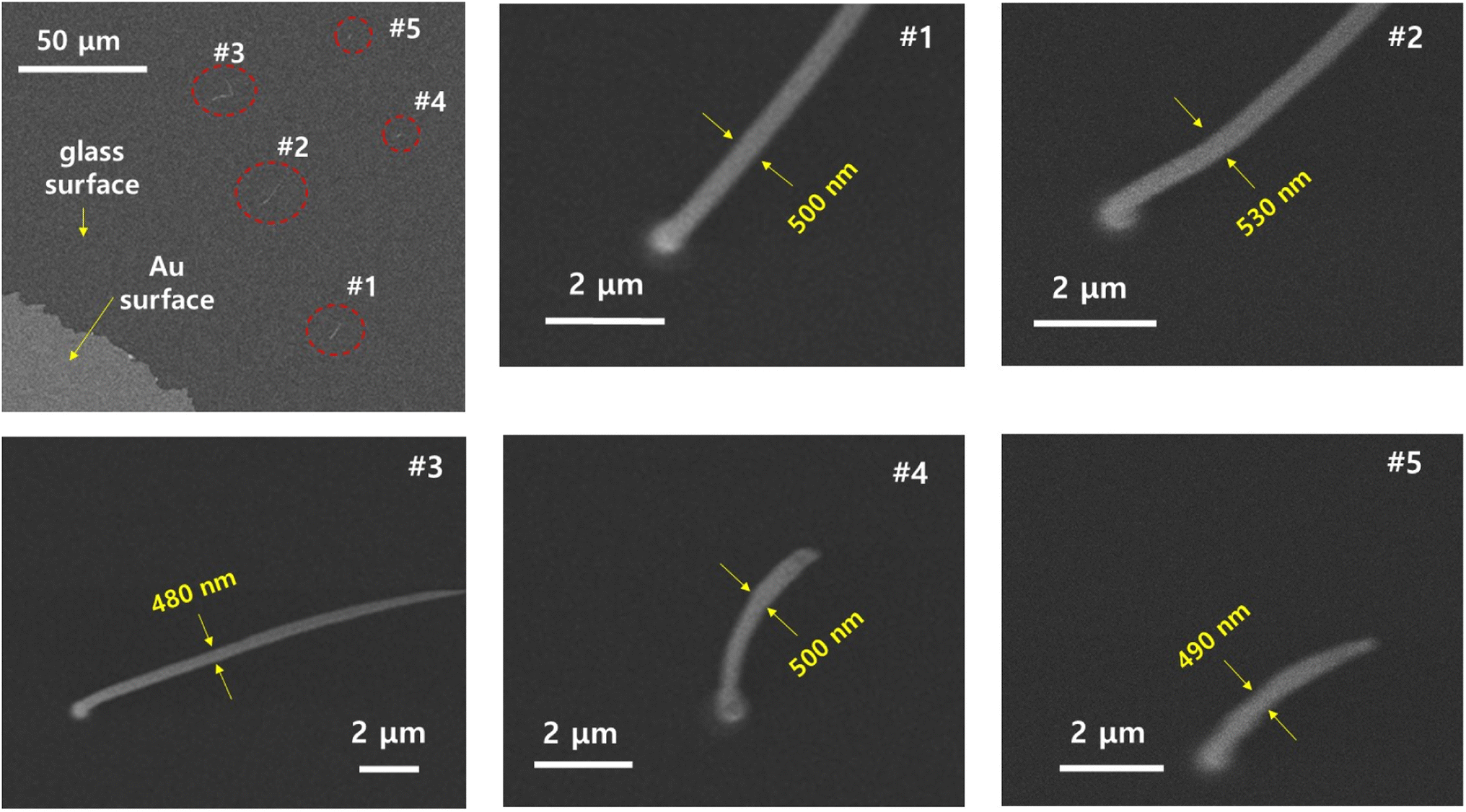 | ||
| Fig. 4 SEM images of CdSe QD wires fabricated using the pulled micropipette-combined AFM system. Wires #1–#3 are laid down, and wires #4 and #5 are standing vertically but tilted in one direction. All fabricated CdSe QD wires have a diameter of about 500 nm corresponding to the aperture diameter of the micropipette. | ||
Even though the small volume of liquid evaporates quickly during the retraction step of the fabrication process, liquid still exists inside the fabricated CdSe QD wires, making them a composite material. Thus, we investigated the evaporation behavior with laser irradiation on the fabricated CdSe QD wires for heat injection. First, as shown in Fig. 5a, we performed laser irradiation (532 nm wavelength) near the middle section of 3D printed CdSe QD wire #3, which was laid down on the substrate (Fig. 4). We observed a bending of the wire by the laser irradiation-induced evaporation of the liquid inside. Next, as shown in Fig. 5b we performed laser irradiation near the root region of the vertically sustained wire #4 (Fig. 4), which caused it to fall in the direction of its lean. We also tested laser irradiation on the top region of the other vertically sustained sample, wire #5, and found that wire fell with an intended direction according to the laser irradiation direction, as shown in Fig. 5c. We conjecture that this phenomenon may be due to the optical force exerted on the top of the fabricated wire following a mechanism different from the evaporation mechanism. In the process of QD wire printing, the starting point of the nanowire is printed while attached to the surface of the sample. Although it is difficult to check the exact degree of adhesion between the wire bottom and the substrate, we assume that degree of adhesion might be enough to detach the wire from the substrate by a method to lightly touch the wire using the pipette tip after printing, a method to rapidly move the pipette in the x- or y-axis direction after finishing fabrication, or a method to heat the starting point with a laser like this experiment. Namely, it is judged that the bonding degree of the wire surface and the surface is the degree that can be knocked down with an appropriate external force. Therefore, the printed wire can fall off the surface of the sample under the action of a moderate external force.
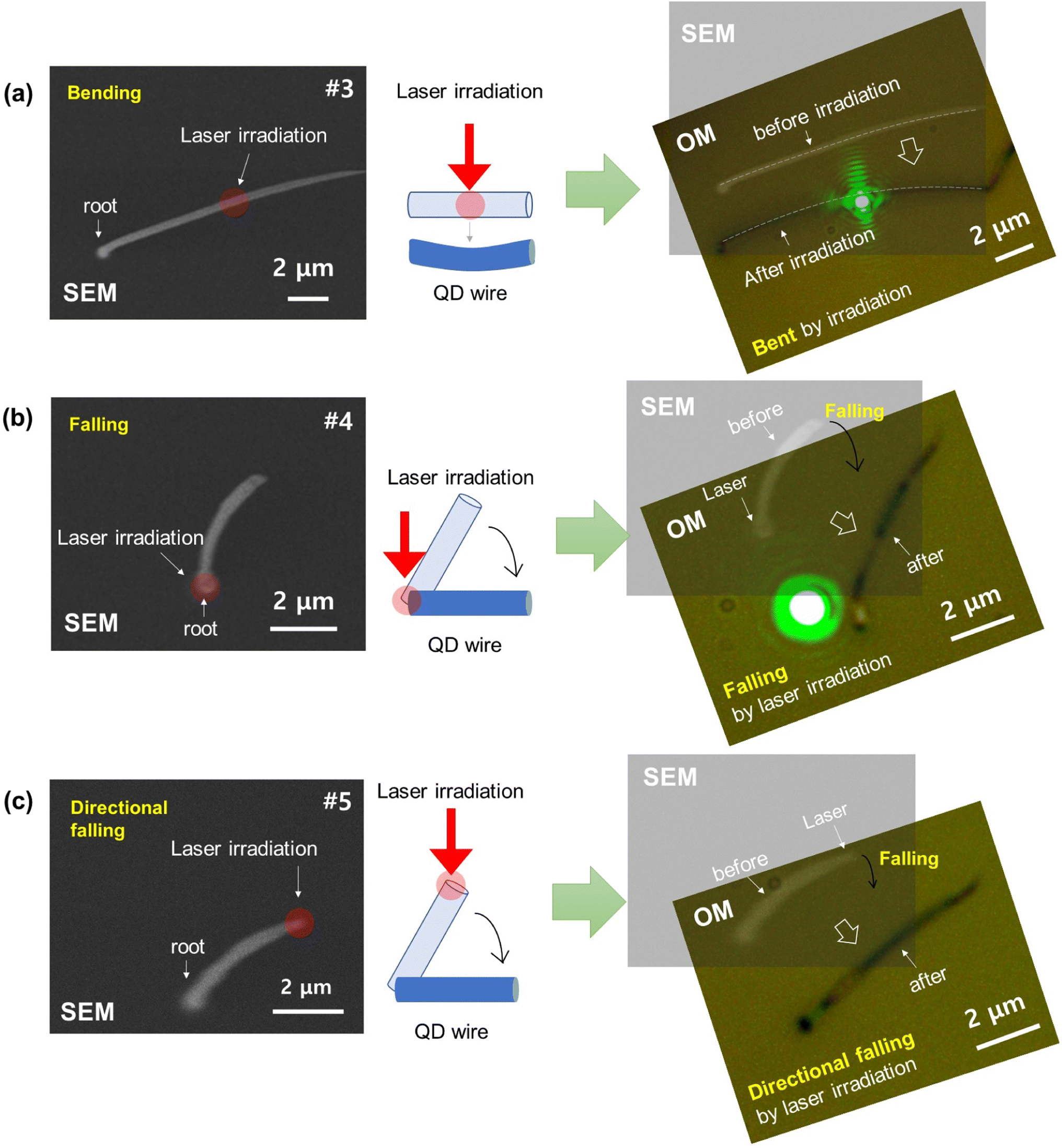 | ||
| Fig. 5 Evaporation behaviors of 3D printed CdSe QD wires by laser irradiation including directional falling. (a) Bending by laser irradiation on the middle of a CdSe QD wire laid horizontally. Dotted lines in the right panel indicate the bending degree of before (SEM image) and after (OM image) irradiation. (b) Falling by laser irradiation on the root of a CdSe QD wire standing vertically with a lean. (c) Directional falling by laser irradiation on the top of a CdSe QD wire standing vertically with a lean. | ||
To investigate the PL characteristics of the fabricated CdSe QD wires, we performed hyperspectral measurements, where images collected at different wavelengths over the same spatial area provide hyperspectral cube data. Hyperspectral cube data consist of two spatial dimensions and one spectral dimension. A hyperspectral imaging system was used to obtain the spatial PL intensity of the fabricated CdSe QDs as a function of emission wavelength. A 405 nm continuous wavelength laser was used as the laser source. The fabricated sample substrate was placed on an inverted optical microscope (Nikon eclipse Ti), and the laser was focused on the sample by a 100× objective lens (NA, x 0.9, Nikon) with 400 nm resolution. PL signals were obtained using an electron multiplying charge-coupled device (EMCCD) (iXon3, DU-89E-C00-#BV) with a hyperspectral imager (photon etc., IM0002400001) placed in front of the EMCCD. Before measurement of the fabricated CdSe QD wires, we applied a single droplet of CdSe solution on the glass substrate and measured the PL of the droplet, which showed a clear resonance peak typical of CdSe QDs near 588 nm as a reference (Fig. 6a). We then fabricated a CdSe QD wire with a length of 3.33 μm and width of 0.56 μm using the pulled micropipette-combined AFM system as a nanoscale 3D printing scheme and measured its PL emission (Fig. 6b). Fig. 6a-(i) and b-(i) show optical images of the patterned CdSe wire. As shown in Fig. 6b, the PL emission of the patterned CdSe wire, depending on its position, can be easily identified in the PL intensity mapping, where the PL intensity mapping image in Fig. 6b-(ii) shows no PL emission in the non-printed area, indicating that the wire was successfully patterned. The PL emission spectra obtained from the emission area shows an emission wavelength of 588 nm, which is almost identical to the bare CdSe QDs. This result indicates that 3D printing with a pulled micropipette does not affect the optical characteristics of the patterned CdSe QDs.
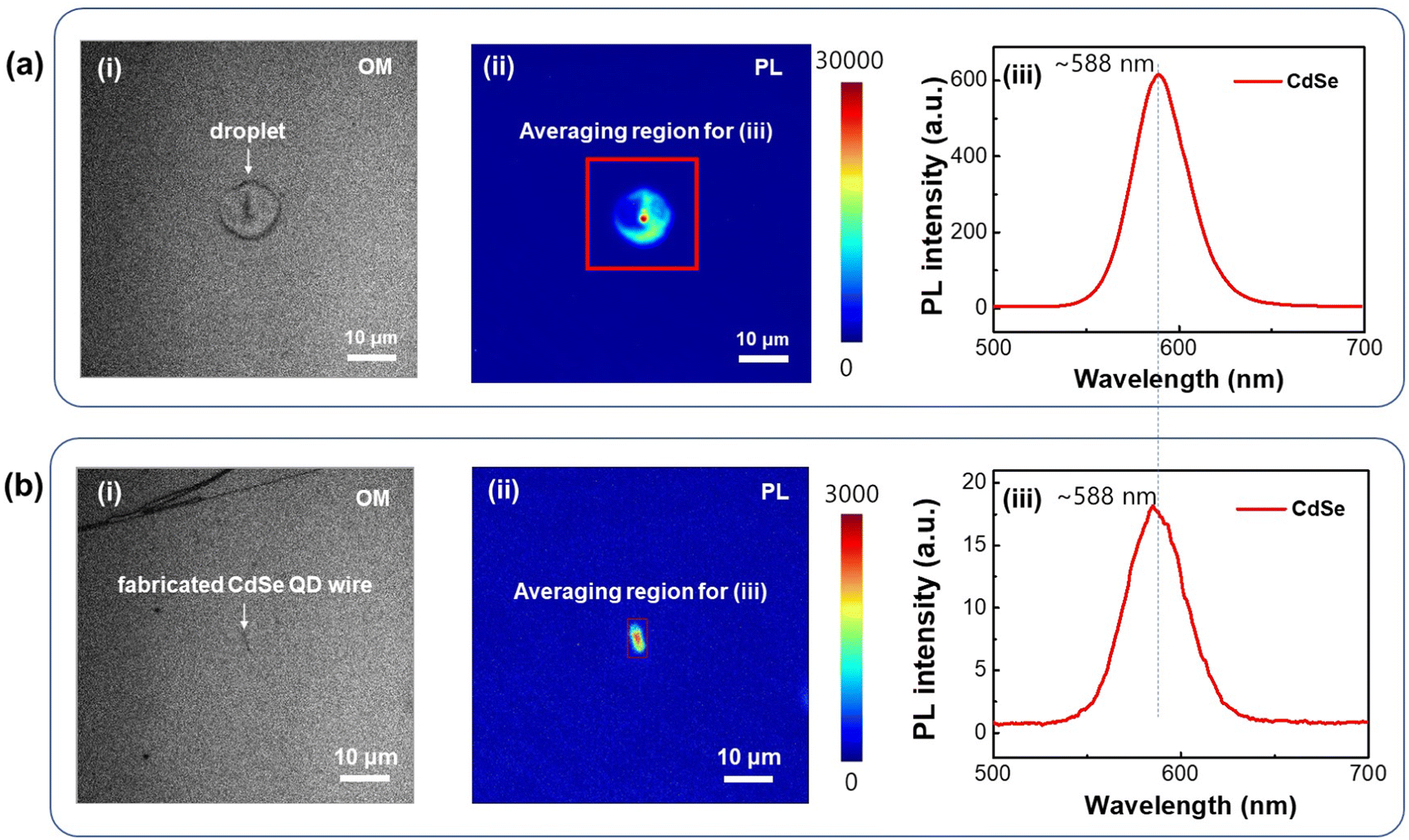 | ||
| Fig. 6 Photoluminescence (PL) emission of the reference (droplet) and the fabricated CdSe QD wire. (a and b) Optical image (i), hyperspectral PL intensity mapping image (ii), and average PL response (iii) from the red box in (ii) of a low volume droplet of CdSe QD solution (a) and the fabricated CdSe QD wire (b). The images are scaled from 0 to 3000 (b) and 0 to 30000 (a) CCD counts to show which sections appear brighter. | ||
Following the above analyses, we additionally carried out Raman measurements at room temperature in backscattering geometry. Here, we cannot easily obtain Raman signals from the fabricated 500 nm diameter CdSe QD wires for the following reasons. Because the fabrication process is based on a streaking of QD particles from the pipette along the substrate while the liquid evaporates during the retraction of the tip, the density of the applied QDs is not uniform, and there may even be empty spots with no QDs due to the different dispersion profiles of QD solution inside of the pipette near the tip apex. Moreover, the QD counts within 500 nm may be insufficient to obtain a sufficiently high intensity required for far-field Raman measurement. Thus, we used a relatively big pen-shaped pipette with an aperture diameter of about 2.2 μm (inset of left graph in Fig. 7a) to fabricate CdSe QD wires with a diameter of about 2 μm, after which we measured the Raman signals. The samples were placed on a computer-controlled transitional XY stage for the mapping measurements. An Ar-ion laser with a wavelength of 514.5 nm was focused on the wire surface using an optical microscope objective lens (100×/0.90 NA) with spatial resolution better than 1 μm. The scattered light from the QD wire was dispersed through a monochromator using a 1200 grooves per mm grating and recorded using a thermoelectrically cooled CCD detector. The accumulation time for each Raman spectrum was 30 s. Fig. 7a shows representative Raman spectra obtained from four different QD wires. A Raman signal from the CdSe QDs was only observed for wire #4. The 206 cm−1 mode corresponds to the first-order longitudinal optical (LO) phonon of the CdSe QDs embedded in the wire.25,26 In addition, the Raman spectrum shows a broad background that corresponds to the QD PL. To investigate the uniformity of QD density in a single wire, Raman line scan measurements were performed along the long axis of wire #4. Fig. 7b shows that the QD LO phonon signals are more intense at the bottom and the top regions of the wire, indicating that the pipette retraction period or retraction speed might affect the accumulated QD density in the solution during wire formation through the open aperture of the micropipette.
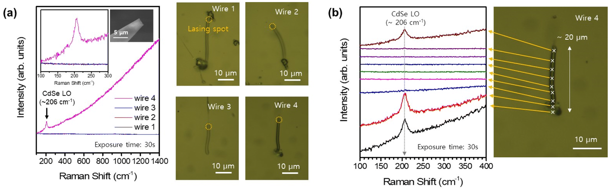 | ||
| Fig. 7 Raman spectroscopy results of the fabricated CdSe QD wires. (a) Left panel: Representative Raman spectra obtained from the tip regions of QD wires. Right panel: optical microscope images of the QD wires. Each probing region is marked by a dotted circle. (b) Left panel: spatially resolved Raman spectra along the long axis of QD wire #4 shown in (a). Right panel: optical microscope image of wire #4 with each probe spot marked with a cross mark. The length of wire #4 is approximately 20 μm, which can be controlled by the retraction timing (the period of time from first ejection to retraction that gives the wire length) of the pipette from the substrate. | ||
Conclusion
We devised a scheme for the fabrication of 3D printed CdSe QD wires using an AFM-combined micropipette. We investigated their intrinsic properties with PL measurements and Raman spectroscopy and found that vertically sustained wires following fabrication via the 3D printing scheme can be controlled by laser irradiation in terms of directional falling by heat injection or optical force. We have a plan to perform various types of the QD wires by using the AFM-guided microscale and nanoscale 3D printing scheme with another particle solutions, such as CdZnSe, CdS, even perovskite QD solution. These may have useful characteristics with high density profile of the particles giving good optical and different energy band structures. From the results of this study, the developed technique for the vertical growth or lateral drawing of QD wires can be adopted in display applications or investigations into semiconducting properties or the coexistence phase of QD–liquid mixtures in 1D nanoscale objects, taking advantage of the directional control of the small size of the materials via the optical force or evaporation phenomenon.Author contributions
Taesun Yun: methodology, writing – original draft. Yong Bin Kim, Taegeon Lee, Hyeongwoo Lee: methodology, writing. Heesuk Rho, Kyoung-Duck Park: investigation, writing – review & editing. investigation, Hong Seok Lee, Sangmin An: conceptualization, methodology, investigation, writing – original draft, review & editing, supervision.Conflicts of interest
The authors declare no conflict of interest.Acknowledgements
The authors declare that they have no known funding source that could have appeared to influence the work reported in this paper. This work was supported by National Research Foundation of Korea (NRF) grants funded by the Korean government (MSIT) (2022R1A4A1033358, 2021R1A2C1003074), (MEST) (2019K2A9A1A06099937, 2020R1C1C1011301, 2020R1I1A1A01070755), by a National Research Council of Science & Technology (NST) grant by the Korean government (MSIT) (CRC-20-01-NFRI), and by the Ministry of Trade, Industry and Energy (MOTIE, 20019223) and Korea Institute for Advancement of Technology (KIAT) through the International Cooperative R&D program (P0019625).References
- C. Darkes-Burkey and R. F. Shepherd, High-resolution 3D printing in seconds, Nature, 2020, 588, 594–595 CrossRef CAS.
- M. Regehly, Y. Garmshausen, M. Reuter, N. F. König, E. Israel, D. P. Kelly, C.-Y. Chou, K. Koch, B. Asfari and S. Hecht, Xolography for linear volumetric 3D printing, Nature, 2020, 588, 620–624 CrossRef CAS.
- J. H. Martin, B. D. Yahata, J. M. Hundley, J. A. Mayer, T. A. Schaedler and T. M. Pollock, 3D printing of high-strength aluminium alloys, Nature, 2017, 549, 365–369 CrossRef CAS PubMed.
- D. Cyranoski, Science education: Reading writing and nanofabrication, Nature, 2009, 460, 171–172 CrossRef CAS.
- S. Y. Chou, P. R. Krauss and P. J. Renstrom, Imprint lithography with 25-nanometer resolution, Science, 1996, 272(5258), 85–87 CrossRef CAS.
- H. Tang, C. Yang, Z. Lin, Q. Yang, F. Kangac and C. P. Wongbd, Electrospray-deposition of graphene electrodes: a simple technique to build high-performance supercapacitors, Nanoscale, 2015, 7, 9133–9139 RSC.
- W. Hwang, G. Xin, M. Cho, S. M. Cho and H. Chae, Electrospray deposition of polymer thin films for organic light-emitting diodes, Nanoscale Res. Lett., 2012, 7, 52 CrossRef.
- B. D. Gates, Q. Xu, M. stewart, D. Ryan, C. G. Willson and G. M. Whitesides, New Approaches to Nanofabrication: Molding, Printing, and Other Techniques, Chem. Rev., 2005, 105(4), 1171–1196 CrossRef CAS.
- Y. Yan, J. Miao, Z. Yang, F.-X. Xiao, H. B. Yang, B. Liu and Y. Yang, Carbon nanotube catalysts: recent advances in synthesis, characterization and applications, Chem. Soc. Rev., 2015, 44, 3295–3346 RSC.
- X. Zhang, B. Graves, M. De Volder, W. Yang, T. Johnson, B. Wen, W. Su, R. Nishida, S. Xie and A. Boies, High-precision solid catalysts for investigation of carbon nanotube synthesis and structure, Sci. Adv., 2020, 6, 40 Search PubMed.
- D. R. S Cumming, S. Thoms, S. P. Beaumont and J. M. R. Weaver, Fabrication of 3 nm wires using 100 keV electron beam lithography and poly(methylmethacrylate) resist, Appl. Phys. Lett., 1996, 68(3), 322–324 CrossRef.
- M. Remeika and A. Bezryadin, Sub-10 nanometre fabrication: molecular templating, electron-beam sculpting and crystallization of metallic nanowires, Nanotechnology, 2005, 16(8), 1172–1176 CrossRef CAS.
- R. D. Piner, J. Zhu, F. Xu, S. Hong and C. A. Mirkin, Dip-pen nanolithography, Science, 1999, 283(5402), 661–663 CrossRef CAS.
- K. Salaita, Y. Wang and C. A. Mirkin, Applications of dip-pen nanolithography, Nat. Nanotechnol., 2007, 2, 145–155 CrossRef CAS.
- G. Liu, M. Hirtz, H. Fuchs and Z. Zheng, Development of Dip-Pen Nanolithography (DPN) and Its Derivatives, Small, 2019, 15, 1900564 CrossRef PubMed.
- H.-J. Wu, Y.-J. Liu, H.-Q. Li, C. Chen, Y. Dou, H.-F. Lou, M. S. Ho, X.-M. Li, Z. Gao and S. Duan, Analysis of microglial migration by a micropipette assay, Nat. Protoc., 2014, 9, 491–500 CrossRef CAS.
- S. An and W. Jhe, Fabrication and Characterization of Au Nanoparticle-aggregated Nanowires by Using Nanomeniscus-induced Colloidal Stacking Method, Nano-Micro Lett., 2015, 7(1), 27–34 CrossRef CAS.
- S. An, C. Stambaugh, G. Kim, M. Lee, Y. Kim, K. Lee and W. Jhe, Low-volume liquid delivery and nanolithography using a nanopipette combined with a quartz tuning fork-atomic force microscope, Nanoscale, 2012, 4, 6493–6500 RSC.
- F. J. Giessibl, Advances in atomic force microscopy, Rev. Mod. Phys., 2003, 75, 949 CrossRef CAS.
- M. Lee, J. Jahng, K. Kim and W. Jhe, Quantitative atomic force measurement with a quartz tuning fork, Appl. Phys. Lett., 2007, 91, 023117 CrossRef.
- B. Kim, J. Jahng, R. M. Khan, S. Park and E. O. Potma, Eigenmodes of a quartz tuning fork and their application to photoinduced force microscopy, Phys. Rev. B, 2017, 95, 075440 CrossRef.
- H. Choe, M.-H. Hong, Y. Seo, K. Lee, G. Kim, Y. Cho, J. Ihm and W. Jhe, Formation, manipulation, and elasticity measurement of a nanometric column of water molecules, Phys. Rev. Lett., 2005, 95, 187801 CrossRef CAS.
- S. Kim, D. Kim, J. Kim, S. An and W. Jhe, Direct Evidence for Curvature-Dependent Surface Tension in Capillary Condensation: Kelvin Equation at Molecular Scale, Phys. Rev. X, 2018, 8, 041046 Search PubMed.
- W. Bak, B. Sung, J. Kim, S. Kwon, B. Kim and W. Jhe, Time-resolved observation of thermally activated rupture of a capillary-condensed water nanobridge, Appl. Phys. Lett., 2015, 106(1), 013102 CrossRef.
- F. Todescato, A. Minotto, R. Signorini, J. J. Jasieniak and R. Bozio, Investigation into the Heterostructure Interface of CdSe-Based Core–Shell Quantum Dots Using Surface-Enhanced Raman Spectroscopy, ACS Nano, 2013, 7, 6649–6657 CrossRef CAS PubMed.
- J. H. Kim, H. Kim, H. Rho, Y.-J. Choi and J.-G. Park, Resonant and polarized Raman scattering from single CdS/CdSe core–shell nanowires, J. Phys. D: Appl. Phys., 2014, 47, 135104 CrossRef.
Footnote |
| † Electronic supplementary information (ESI) available. See DOI: https://doi.org/10.1039/d2na00627h |
| This journal is © The Royal Society of Chemistry 2023 |