
 Open Access Article
 This Open Access Article is licensed under a Creative Commons Attribution-Non Commercial 3.0 Unported Licence
Nanostructure-induced L10-ordering of twinned single-crystals in CoPt ferromagnetic nanowires†
Ryo
Toyama
 a,
Shiro
Kawachi
bcd,
Jun-ichi
Yamaura
bc,
Takeshi
Fujita
e,
Youichi
Murakami
c,
Hideo
Hosono
b and
Yutaka
Majima
*ab
a,
Shiro
Kawachi
bcd,
Jun-ichi
Yamaura
bc,
Takeshi
Fujita
e,
Youichi
Murakami
c,
Hideo
Hosono
b and
Yutaka
Majima
*ab
aLaboratory for Materials and Structures, Institute of Innovative Research, Tokyo Institute of Technology, Yokohama, Kanagawa 226-8503, Japan. E-mail: majima@msl.titech.ac.jp
bMaterials Research Center for Element Strategy, Tokyo Institute of Technology, Yokohama, Kanagawa 226-8503, Japan
cInstitute of Materials Structure Science, High Energy Accelerator Research Organization (KEK), Tsukuba, Ibaraki 305-0801, Japan
dGraduate School of Science, University of Hyogo, Kamigori, Hyogo 678-1297, Japan
eSchool of Environmental Science and Engineering, Kochi University of Technology, Kami, Kochi 782-8502, Japan
First published on 6th October 2022
Abstract
L10-ordered ferromagnetic nanowires with large coercivity are essential for realizing next-generation spintronic devices. Ferromagnetic nanowires have been commonly fabricated by first L10-ordering of initially disordered ferromagnetic films by annealing and then etching them into nanowire structures using lithography. If the L10-ordered nanowires can be fabricated using only lithography and subsequent annealing, the etching process can be omitted, which leads to an improvement in the fabrication process for spintronic devices. However, when nanowires are subjected to annealing, they easily transform into droplets, which is well-known as Plateau–Rayleigh instability. Here, we propose a concept of “nanostructure-induced L10-ordering” of twinned single-crystals in CoPt ferromagnetic nanowires with a 30 nm scale ultrafine linewidth on Si/SiO2 substrates. The driving forces for nanostructure-induced L10-ordering during annealing are atomic surface diffusion and extremely large internal stress at ultrasmall 10 nm scale curvature radii of the nanowires. (Co/Pt)6 multilayer nanowires are fabricated by a lift-off process combining electron-beam lithography and electron-beam evaporation, followed by annealing. Cross-sectional scanning transmission electron microscope images and nano-beam electron diffraction patterns clearly indicate nanostructure-induced L10-ordering of twinned single-crystals in the CoPt ferromagnetic nanowires, which exhibit a large coercivity of 10 kOe for perpendicular, longitudinal, and transversal directions of the nanowires. Two-dimensional grazing incidence X-ray diffraction shows superlattice peaks with Debye–Scherrer ring shapes, which also supports the nanostructure-induced L10-ordering. The fabrication method for nanostructure-induced L10-ordered CoPt ferromagnetic nanowires with twinned single-crystals on Si/SiO2 substrates would be significant for future silicon-technology-compatible spintronic applications.
1. Introduction
Ferromagnetic nanowires have great potential for ultrahigh-density data storage applications, such as magnetic domain-wall racetrack memory and perpendicular magnetic recording,1–9 as well as for spintronic sensors,10–17 spin torque oscillators,18,19 excitation of spin waves,20,21 spinmotive force devices,22,23 and biomedical applications.24,25 In magnetic domain-wall racetrack memory, magnetic domains in an array of ferromagnetic nanowires store the data.1–6 Multilayered nanowires with ferromagnetic and non-magnetic layers such as Co/Cu can be used as spintronic sensors based on giant magnetoresistance effect.10–16 Magnetostrictive sensors based on Co nanowires on flexible substrates have also been demonstrated.17In particular, ferromagnetic materials with strong perpendicular magnetocrystalline anisotropy and large coercivity (Hc) are necessary for the nanostructures to be immune to the thermal fluctuation of magnetization above room temperature.26,27 From this perspective, L10-ordered alloys such as CoPt are considered to be promising candidates, where L10-ordering of CoPt is obtained through the phase transformation from the A1-disordered phase by thermal treatment.28–31
To fabricate L10-CoPt, epitaxial growth technique and management of lattice-mismatch-induced strain on single-crystal insulating substrates such as MgO(001) have been widely utilized.32,33 Combining these with annealing allows for a facile fabrication of perpendicularly-magnetized tetragonal L10-CoPt films possessing alternating monoatomic layers of Co and Pt towards the direction normal to the substrates.32,33 Moreover, the L10-ordering has reportedly been enhanced by rapid thermal annealing (RTA), where the in-plane tensile stress between ferromagnetic thin film and substrate, which is induced by the high heating rate of RTA, contributed to the high degree of L10-ordering.34–42 After fabricating L10-CoPt thin films based on these growth techniques, nanowire structures have been commonly prepared using lithography and finally etching the ordered films.43
Recently, we have developed a fabrication process for Pt-based nanogap electrodes by a lift-off process that combines electron-beam lithography (EBL) and electron-beam (EB) evaporation.44–49 Pt-based nanogap electrodes with an ultrafine linewidth of 10 nm were successfully fabricated by optimizing the fabrication conditions.44
We also reported the L10-ordering of Co/Pt multilayer thin films on thermally oxidized Si (Si/SiO2) substrates by EB evaporation and annealing processes, which was characterized by scanning electron microscope (SEM), grazing incidence X-ray diffraction (GI-XRD), and vibrating sample magnetometer (VSM).50–52 In Pt (6.6 nm)/Co (4.8 nm) bilayer thin films, graded films consisting of L12-ordered CoPt3, L10-CoPt, and L12-ordered Co3Pt were formed during interdiffusion of the bilayer annealed at 800 °C for 30 s by RTA in a vacuum.50 Because the interdiffusion and L10-ordering of CoPt were in progress owing to the short annealing time of 30 s RTA process and both L12-CoPt3 and L12-Co3Pt do not usually show large Hc, an Hc in the graded films was as small as 2.1 kOe.50 In [Co (1.2 nm)/Pt (1.6 nm)]4 multilayer thin films, isolated round grains of single-phase L10-CoPt were formed after annealing in a vacuum at 900 °C for approximately 60 min, which exhibited an improved Hc of 2.7 kOe due to the sufficient interdiffusion by multilayered structure and extended annealing time.51 Moreover, we also showed that hydrogen annealing contributed to the enhanced Hc of L10-CoPt.52 After annealing of the (Co/Pt)4 multilayer thin films at 800 °C for 60 min, a maximum Hc of 13.3 kOe was obtained in L10-CoPt, which exhibited angular-outline isolated grain structures.52
If the nanowires can be directly fabricated Si/SiO2 substrates by first using lithography and then L10-ordering of initially disordered ferromagnetic films by annealing, the etching process can be omitted, which leads direct fabrication process of spintronic devices on Si/SiO2 substrates. Direct fabrication of L10-CoPt nanowires on Si/SiO2 substrates using only lithography and subsequent annealing can be beneficial for the future integration of non-volatile spintronics with silicon-technology-based complementally metal-oxide semiconductor (CMOS) integrated circuits.53,54 This integration will pave the way for the realization of CMOS-compatible multifunctional nanodevices utilizing both the charge and spin of an electron.55–59
To achieve the fabrication of L10-CoPt nanowires on Si/SiO2 substrates, two challenges remain: the establishment of a fabrication process for CoPt ferromagnetic nanowires with linewidths less than a few tens of nanometers and the L10-ordering process of CoPt nanowires on Si/SiO2 substrates. For integrated spintronic device applications, the linewidth of ferromagnetic nanowires is preferably as narrow as possible. Several fabrication processes for ferromagnetic nanowires have been reported, such as etching, electrodeposition, focused-electron-beam-induced deposition, and lift-off processes.43,60–63L10-FePt nanowires with linewidths ranging from 2 μm to 30 nm have been fabricated by first depositing 10 nm-thick L10-FePt layer on single-crystal MgO(001) substrates and then etching by means of EBL and ion milling techniques.63 Electrodeposition on anodized aluminum oxide templates have yielded perpendicularly aligned L10-CoPt nanowires with diameters of 20–200 nm and some of these nanowires exhibited a large Hc over 10 kOe.64–73
However, in nanostructures below a few tens of nanometers, there is an extremely large internal stress, which is inversely proportional to the 10 nm-scale curvature radii and proportional to the surface tension, according to Young–Laplace equation given by:74–76
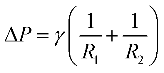 | (1) |
In this paper, we propose a concept of “nanostructure-induced L10-ordering” of twinned single-crystals in CoPt ferromagnetic nanowires with a 30 nm scale ultrafine linewidth on Si/SiO2 substrates, where the atomic interdiffusion, surface diffusion, and extremely large internal stress at ultrasmall 10 nm scale curvature radii of the nanowires during annealing are the driving forces for nanostructure-induced L10-ordering. The ordering mechanism in the nanowires in this study is different from previous studies. Nanostructure-induced L10-ordering of CoPt ferromagnetic nanowires would be realized by fabricating CoPt nanowires with a 30 nm scale narrow linewidth on Si/SiO2 substrates using only lithography and utilizing annealing. We demonstrate the proof-of-concept of nanostructure-induced L10-ordering method for fabricating twinned single-crystals in CoPt ferromagnetic nanowires on Si/SiO2 substrates by a lift-off process combining EBL and EB evaporation, followed by annealing. The surface morphologies, crystal structures, magnetic properties, and cross-sectional profiles of the nanowires are analyzed by SEM, GI-XRD, VSM, and transmission electron microscope (TEM), respectively.
2. Results and discussion
Fig. 1 shows typical top-view SEM images of the CoPt nanowires before and after annealing at 650 °C for 90 min. The annealed nanowires showed linewidths of 20–30 nm without disconnection of the nanowire structures (Fig. 1b). Linewidth perturbation was also observed for the annealed nanowires (Fig. 1b). Moreover, Fig. S1† shows the SEM images of the CoPt nanowires after annealing for 30 and 60 min, which also exhibited nanowire structures without disconnection after annealing.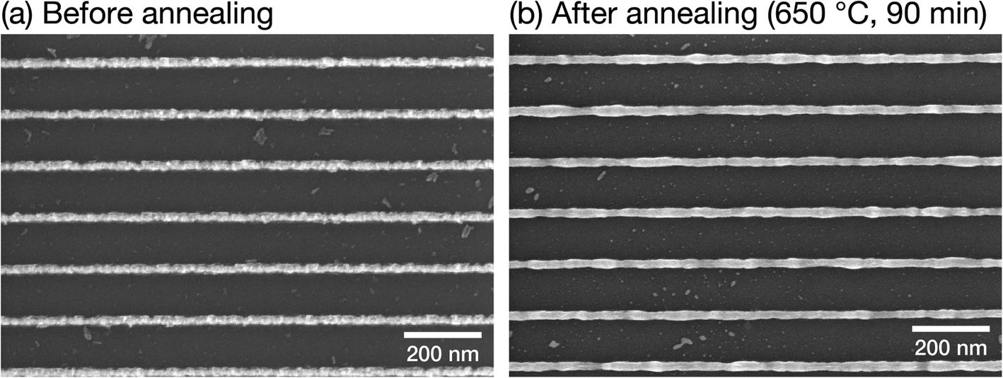 | ||
| Fig. 1 Typical top-view scanning electron microscope (SEM) images of [Co (3.6 nm)/Pt (4.8 nm)]6 multilayer nanowires on Si/SiO2 substrates (a) before and (b) after annealing at 650 °C for 90 min. The SEM images of CoPt nanowires after annealing at 650 °C for 30 and 60 min are shown in Fig. S1.† | ||
The two-dimensional (2D) GI-XRD pattern of the CoPt nanowires after annealing at 650 °C for 90 min is shown in Fig. 2. The pattern was obtained by subtracting the background signal of Si/SiO2 substrates from the pattern of the nanowires on the substrates. From the subtracted 2D GI-XRD pattern (Fig. 2), superlattice peaks of L10-CoPt 001 and 110 were clearly observed, indicating the L10-ordering of the CoPt nanowires after annealing. The peak shapes of L10-CoPt 001 and 110 were Debye–Scherrer rings (Fig. 2), which indicates that the c-axis of L10-CoPt tended to be oriented perpendicular to the curved surface of the nanowires. Moreover, the other superlattice peaks of L10-CoPt 201 and 112 and the fundamental peaks of 111, 220, and 311 were also clearly observed (Fig. 2). The nanostructure induced L10-ordering of the nanowires was also confirmed after annealing for 30 and 60 min, as evident in the superlattice peaks of L10-CoPt 001 and 110 with Debye–Scherrer ring shapes (Fig. S2†). The intensity of the L10-CoPt 001 peak of the nanowires became stronger for longer annealing times (Fig. S2†). On the other hand, the full-width at half maximum of L10-CoPt 001 became smaller for longer annealing times (Fig. S2†).
 | ||
| Fig. 2 Two-dimensional (2D) grazing incidence X-ray diffraction (GI-XRD) pattern of (Co/Pt)6 nanowires on Si/SiO2 substrates after annealing at 650 °C for 90 min. The diffraction peaks of L10-CoPt (001, 110, 111, 200, 201, 112, 220, and 311) are indicated by red arrows. The 2D GI-XRD patterns of the nanowires after annealing at 650 °C for 30 and 60 min are shown in Fig. S2.† | ||
The intensity–2θ one-dimensional (1D) GI-XRD profiles of the CoPt nanowires after annealing at 650 °C for 90 min are shown in Fig. 3. The 2θ values for L10-CoPt 001 and 110 were 16.450° and 22.722°, respectively. Therefore, the c and a values for the L10-CoPt nanowires were determined to be c = 3.6804 Å and a = 3.7799 Å, respectively, which agrees with values in the literature.32,50–52,68,70,91
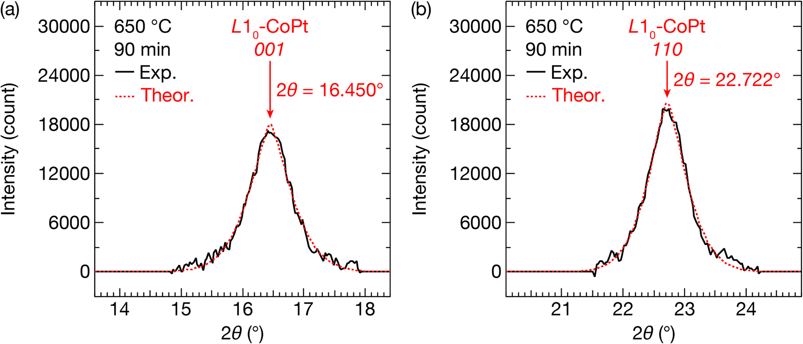 | ||
| Fig. 3 Intensity–2θ 1D GI-XRD profiles of (Co/Pt)6 nanowires on Si/SiO2 substrates after annealing 650 °C for 90 min. Each of the experimental peaks (black curve) of (a) L10-CoPt 001 and (b) L10-CoPt 110 was analyzed by a bell-shaped function after subtracting the remaining background signal. These theoretical curves are plotted as red dotted curves. | ||
The magnetic hysteresis loops (M–H curves) of the nanowires after annealing at 650 °C for 90 min are shown in Fig. 4. The Hc of the annealed nanowires in the transversal (Hc∟), longitudinal (Hc‖), and perpendicular (Hc⊥) directions were 10.6, 10.7, and 10.8 kOe, respectively, which indicates that the nanowires showed an identical Hc value for the three measured directions (Fig. 4).
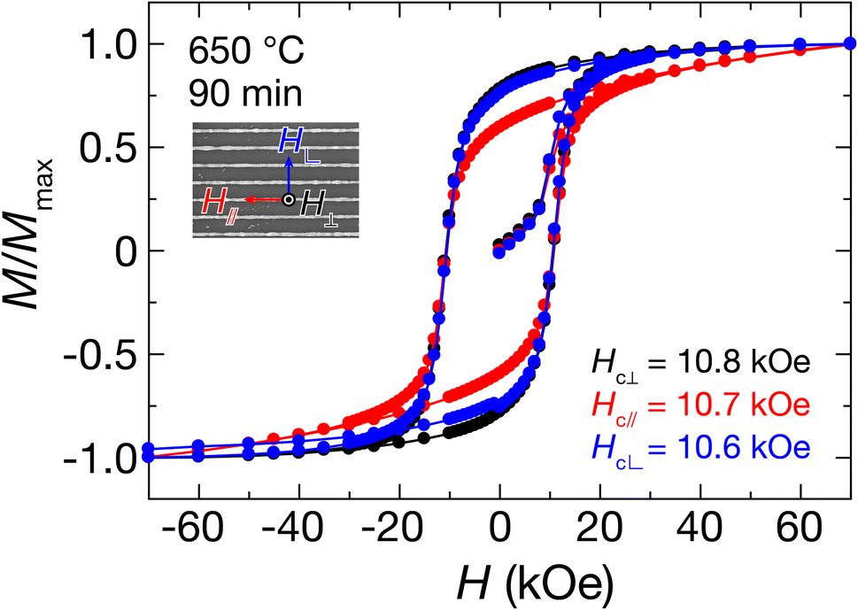 | ||
| Fig. 4 Magnetic hysteresis loops (M–H curves) of (Co/Pt)6 nanowires on Si/SiO2 substrates after annealing at 650 °C for 90 min. M–H curves were measured in a vacuum at room temperature (27 °C) by applying a magnetic field in the out-of-plane direction (perpendicular; black curves and filled circles), in-plane direction parallel to the nanowire-axis (longitudinal; red curves and filled circles), and in-plane direction perpendicular to the nanowire-axis (transversal; blue curves and filled circles). Hc⊥, Hc∥, and Hc∟ represent Hc for perpendicular, longitudinal, and transversal directions, respectively. | ||
Fig. 5 shows the cross-sectional bright field (BF)-TEM images, high-angle annular dark field (HAADF)-scanning transmission electron microscope (STEM) images, and nano-beam electron diffraction (NED) pattern of the CoPt nanowires after annealing at 650 °C for 90 min, which were observed from the nanowire-axis direction along the [110] zone axis. The nanowires exhibited elliptical cross-sectional shapes with reduced heights compared to the initial total thickness of 50.4 nm (Fig. 5a, b and d). From the NBD pattern (Fig. 5c), superlattice diffraction spots of L10-CoPt 001 and 110 (indicated by the red circles) were observed along with the fundamental spots (indicated by the yellow circles), which indicates L10-ordering of the CoPt nanowires after annealing. From the magnified HAADF-STEM images, alternating monoatomic layers of Co (appeared as dark spots and indicated by the light blue dots) and Pt (appeared as bright spots and indicated by the orange dots) were clearly observed along the [110] zone axis at the top-edge of the nanowires (Fig. 5e) and near the nanowire–substrate interface (Fig. 5f). The twin boundary was clearly observed (indicated by the red dashed line in Fig. 5f). The directions of c-axes of L10-CoPt with twin planes at the top-edge and the nanowire–substrate interface are indicated as white and green arrows in Fig. 5e and f.
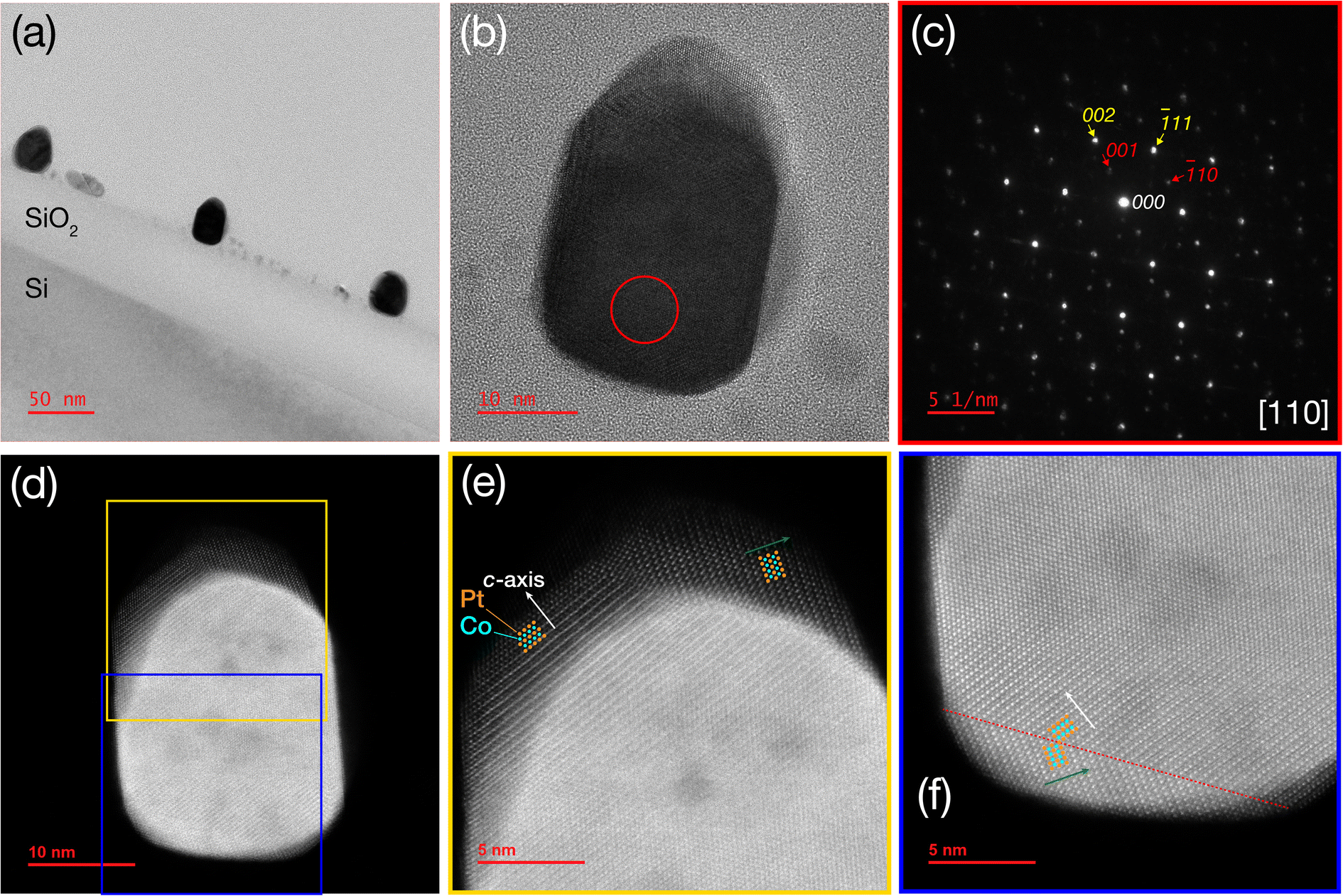 | ||
| Fig. 5 Cross-sectional (a) bright field (BF)-TEM image, (b) magnified BF-TEM image, (c) nano-beam electron diffraction (NED) pattern, taken at the red circle in part (b), (d) high-angle annular dark field (HAADF)-scanning transmission electron microscope (STEM) image, and (e and f) magnified HAADF-STEM images of part (d) [(orange square for part (e) and red square for part (f))] of (Co/Pt)6 nanowires on Si/SiO2 substrates after annealing at 650 °C for 90 min, which were observed from the nanowire-axis direction along the [110] zone axis. In part (c), the superlattice diffraction spots of L10-CoPt are indicated by the red arrows, whereas the fundamental spots are indicated by the yellow arrows. In parts (e) and (f), Co and Pt atoms are indicated by the light blue and orange dots, respectively, and the directions of c-axes of L10-CoPt are shown as white and green arrows. The twin boundary is indicated by red dashed line in part (f). | ||
The TEM images, HAADF-STEM images, and NED pattern, which were observed from parallel to the nanowire-axis along the [110] zone axis, are shown in Fig. 6. From the BF-TEM image (Fig. 6a), even though the height of L10-CoPt nanowire varied in the range of 25–40 nm, Plateau–Rayleigh instability was well suppressed and the nanowire structure maintained after annealing. The annealed nanowires consisted of a chain of multidomain grains (Fig. 6a). The NED pattern (Fig. 6c) at the center of the grain showed superlattice diffraction spots of L10-CoPt 001 and 110 (indicated by the red circles) along with the fundamental spots (indicated by the yellow circles), which indicates nanostructure-induced L10-ordering of the CoPt nanowires after annealing. Furthermore, the HAADF-STEM image (Fig. 6d) showed alternating monoatomic layers of Co (appeared as dark spots and indicated by the light blue dots) and Pt (appeared as bright spots and indicated by the orange dots), where the c-axis of L10-CoPt was tilted with respect to the substrate normal. Twins with (110) twin planes were also clearly observed; the twin boundary is indicated by the red dashed lines in Fig. 6d.
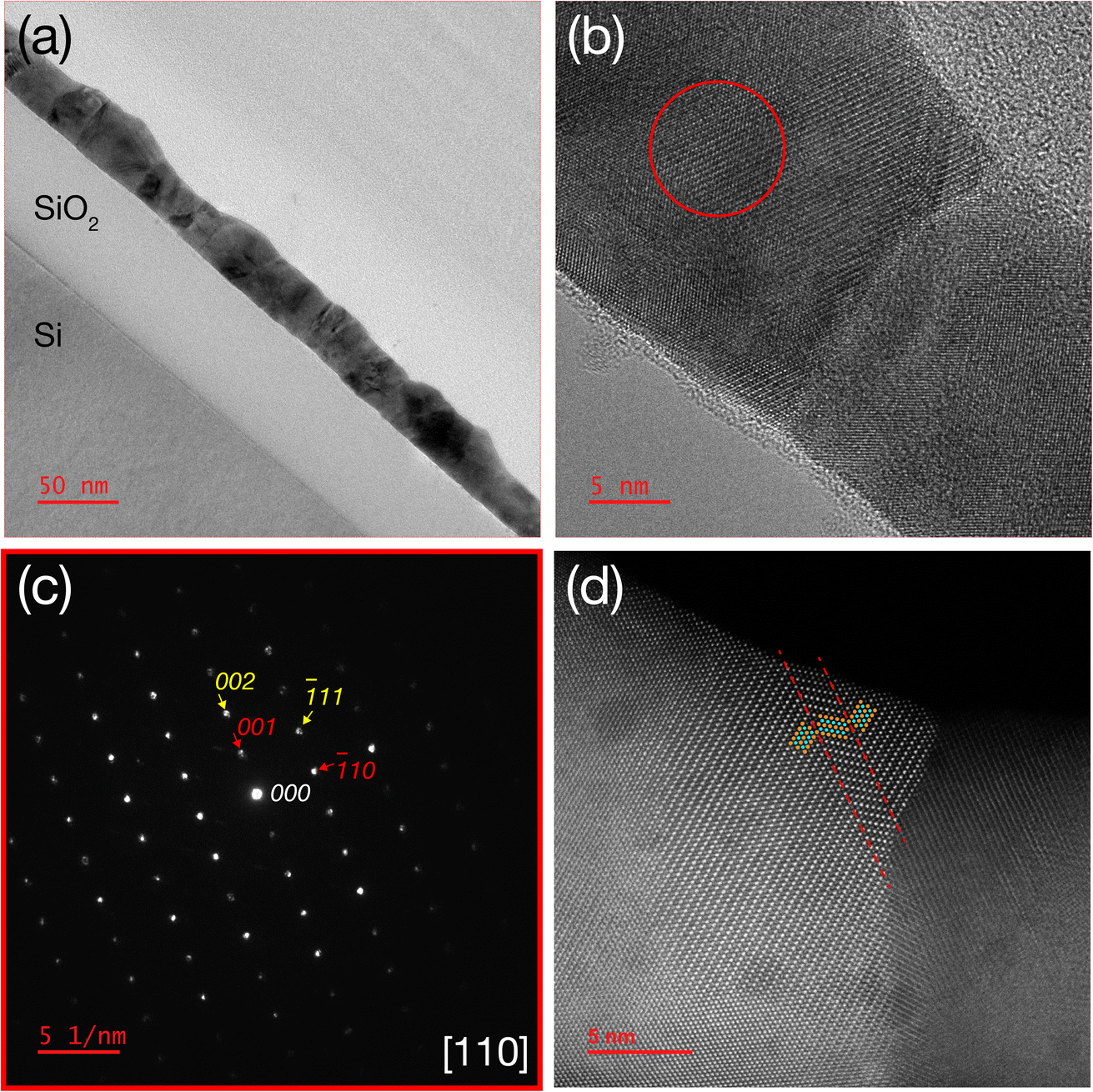 | ||
| Fig. 6 Cross-sectional (a) BF-TEM image, (b) magnified BF-TEM image, (c) NED pattern, taken at the red circle in part (b), and (d) HAADF-STEM image of (Co/Pt)6 nanowires on Si/SiO2 substrates after annealing at 650 °C for 90 min, which were observed from parallel to the nanowire-axis along the [110] zone axis. In part (c), the superlattice diffraction spots of L10-CoPt are indicated by the red arrows, whereas the fundamental spots are indicated by the yellow arrows. In part (d), Co and Pt atoms are indicated by the light blue and orange dots, respectively. The twin boundaries are indicated by red dashed lines in part (d). | ||
The experimental results obtained from SEM, GI-XRD, VSM, NED, and TEM show the nanostructure-induced L10-ordering of twinned single-crystals in CoPt ferromagnetic nanowires, with a linewidth of approximately 30 nm and a large Hc over 10 kOe on Si/SiO2 substrates by a lift-off process that combines of EBL and EB evaporation, followed by annealing.
The BF-TEM images clearly showed that the CoPt nanowires consisted of a chain of grains (Fig. 6a). From the cross-sectional HAADF-STEM images, L10-CoPt with alternating monoatomic layers of Co and Pt was observed at both the top-edge and near the nanowire–substrate interface of the nanowires from the nanowire-axis direction (Fig. 5e and f), respectively, and was also observed from parallel to the nanowire-axis (Fig. 6d). The twin planes were clearly observed in Fig. 5f and 6d. Because the NED patterns were taken at the grain slightly near the nanowire–substrate interface (Fig. 5c) and at the center of the grain (Fig. 6c), and the CoPt nanowires with a linewidth of approximately 30 nm possessed not an A1@L10 core–shell but an entirely L10-ordered structure. As the directions of c-axes of L10-CoPt at the top-edge (white and green arrows in Fig. 5e) were the same as those at the nanowire–substrate interface (white and green arrows in Fig. 5f), respectively, the grain should be composed of single-crystals with twin boundaries. Consequently, “nanostructure-induced L10-ordering” of twinned single-crystals in CoPt ferromagnetic nanowires with a 30 nm scale ultrafine linewidth on Si/SiO2 substrates were fabricated by EBL and annealing.
Here, we discuss the mechanism for nanostructure-induced L10-ordering of twinned single-crystals in CoPt ferromagnetic nanowires on Si/SiO2 substrates based on (i) the atomic surface diffusion at the top-edge of the nanowires and (ii) the extremely large internal stress near the nanowire–substrate interface, originating from the 10 nm-curvature of the nanowires. When the (Co/Pt)6 multilayer nanowires were subjected to annealing, Co and Pt atoms diffused on the nanowire surface and interdiffused inside the nanowires, leading to form A1-disordered CoPt alloy nanowires. Considering the initial total thickness (50.4 nm) and the linewidth (30 nm) of the as-fabricated (Co/Pt)6 multilayer nanowires, the initial cross-sectional aspect ratio (height-to-linewidth) of the nanowires was approximately 1.7, which is larger than unity. Thus, Co and Pt atoms at the top-edge of the nanowires diffused towards the sidewall of the nanowire surface so as to minimize the surface free energy. Owing to the extremely large internal stress at the 10 nm-curvature of the nanowires, the surface-diffused Co and Pt atoms began to form L10-CoPt nuclei possessing alternating monoatomic layers of Co and Pt, where the c-axis of L10-CoPt tended to be oriented normal direction to the curved nanowire surface, which is supported by the HAADF-STEM images (Fig. 5e and 6d). As the nanostructure-induced L10-ordering proceeded, the L10-ordering initiated at the nanowire surface progressed both laterally along the curved nanowire surface and towards the core of the nanowires. On the other hand, near the nanowire–substrate interface, extremely large internal stress is also generated perpendicular to the side of the nanowires (transverse direction with respect to the substrate normal), which is inversely proportional to the 10 nm-scale curvature radii and proportional to the surface tension, according to the Young–Laplace equation (eqn (1)). As a result, driving forces for nanostructure-induced L10-ordering should be the atomic surface diffusion and extremely large internal stress, which lead the elliptical cross-sectional shapes of the nanowires with reduced heights in the BF-TEM images (Fig. 5a and b and 6a). Owing to these driving forces of atomic surface diffusion and extremely large internal stress, the L10-CoPt nuclei grow at the surface and toward the core of the grains in nanowires. The perturbation of the linewidth of the annealed CoPt nanowires was observed from the SEM image (Fig. 1b), which also supports the proposed driving forces for nanostructure-induced L10-ordering of twinned single-crystals in CoPt ferromagnetic nanowires.
Within the L10-CoPt grains, twin planes tended to be observed in the HAADF-STEM images (Fig. 5f and 6d). As the nanostructure-induced L10-ordering proceeded, L10-ordered CoPt grains impinged on the neighboring ones, leading to produce L10-ordered single-crystal grains with twin planes. Finally, the CoPt grains were entirely L10-ordered and the nanowires consisted of a chain of L10-ordered twinned single-crystals.
As the c-axis orientation of L10-ordered CoPt single-crystal grains differed between the grains, the superlattice peaks of L10-CoPt 001 and 110 exhibited Debye–Scherrer ring shapes in the 2D GI-XRD pattern (Fig. 2), which indicates that the c-axis of L10-CoPt was randomly tilted with respect to the substrate normal.
Nanostructure-induced L10-ordered CoPt ferromagnetic nanowires showed an identical Hc value of 10 kOe for the perpendicular, longitudinal, and transversal directions in the VSM results (Fig. 4). The direction of easy-axis of magnetization of nanowire structures tends to align along the wire-axis due to shape anisotropy.92 The identical Hc value for the three measured directions of the CoPt nanowires in this study should be attributed to the different directions of easy-axis of magnetization in L10-ordered CoPt ferromagnetic twinned single-crystals.93,94
From the M–H curves in Fig. 4, a magnetic anisotropy field for the longitudinal direction (red curve) was larger than that for transversal (blue curve) and perpendicular (black curve) directions. Because the nanowires consisted of a chain of L10-ordered CoPt ferromagnetic twinned single-crystals, these grains had different directions of easy-axis of magnetization. As a result, the magnetic moment tended to be fluctuated by the neighboring grains, which leads to the larger anisotropy field for the longitudinal direction.
The nanostructure-induced L10-ordering of CoPt nanowires was confirmed at an annealing temperature of 650 °C, where the ordering temperature was lower than that for CoPt films with a large Hc over 10 kOe in our previous study (800 °C).52 The decrease in the nanostructure-induced L10-ordering temperature was attributed to the melting point depression owing to the nanoscale structures,95–106 which leads to nanostructure-induced L10-ordering of CoPt nanowires at lower ordering temperatures compared to that of the thin film structures.
The annealing temperature of 650 °C should be slightly higher than the process temperatures of Si technology. However, if the nanostructure-induced L10-ordering process will be introduced at first and followed usual Si technology processes, the nanostructure-induced L10-ordering process could be used.
As mentioned in the Introduction part, L10-ordered ferromagnetic nanowires have been typically fabricated by means of etching and electrodeposition.43,60–73 However, the fabrication method of our nanostructure-induced L10-ordered ferromagnetic nanowires is different from those of the nanowires in the literature: compared to the nanowires fabricated by etching,63 our nanowires do not require any etching process, which makes the fabrication process for spintronic devices less complicated. In addition, nanostructure-induced L10-ordering method could prepare L10-ordered ferromagnetic nanowires directly on Si/SiO2 substrates without single-crystal substrates such as MgO. The electrodeposited nanowires also require anodized aluminum oxide templates, and tends to anneal higher temperature of 700–800 °C to obtain L10-ordered phase with high Hc.64–73 Consequently, the nanostructure-induced L10-ordering method and the fabricated ferromagnetic nanowires have many advantageous towards future spintronic device application.
The ordering mechanism in nanostructured CoPt and FePt has been studied theoretically and experimentally in terms of free surface, surface segregation, surface diffusion, defect, size, and shape.107–128 For example, L10-ordering has been found to proceed more quickly at the free surfaces than at the core of the nanostructures.120,124 Surface segregation of Pt has been found to regulate the stoichiometry of the inner layers below the top surface, leading to affect the atomic ordering of the core of the nanostructures.112,121 However, most of these studies have focused on the nanoparticles rather than nanowires on solid-state substrates. Thus, our experimental demonstration and proposed mechanism for nanostructure-induced L10-ordering of CoPt ferromagnetic nanowires on Si/SiO2 substrates at the 10 nm-curvature of the nanowires would give an alternative insight into the nanoscale ordering behaviors.
Consequently, we demonstrated the nanostructure-induced L10-ordering method for fabricating twinned single-crystals in CoPt ferromagnetic nanowires with a linewidth of approximately 30 nm on Si/SiO2 substrates by a lift-off process combining EBL and EB evaporation, followed by annealing, which exhibited a large Hc over 10 kOe. The realization of the CoPt ferromagnetic nanowires through nanostructure-induced L10-ordering would provide an alternative method for manufacturing nanoscale spintronic devices on Si/SiO2 substrates. The nanostructure-induced L10-ordering would also offer another L10-ordering route of nanoscale ferromagnetic alloys. The concept of nanostructure-induced L10-ordering could also be applied to other L10-ordered ferromagnetic materials, such as FePt,30,32 FePd,129 CoPd,130 and precious-metal-free FeNi131 and FeCo.132–134 Furthermore, our approach could be applied to other types of materials, leading to emergence of material properties different form their bulk ones, which is driven by the nanostructure itself. This will potentially open up a research field on “nanostructure-induced materials science and engineering”.
3. Conclusions
We demonstrated nanostructure-induced L10-ordering method for fabricating twinned single-crystals in CoPt ferromagnetic nanowires with a 30 nm scale ultrafine linewidth on Si/SiO2 substrates. The ultrasmall 10 nm scale curvature of the nanowires induced L10-ordering, wherein the driving forces were the atomic interdiffusion, surface diffusion, and extremely large internal stress during annealing. (Co/Pt)6 multilayer nanowires were fabricated on Si/SiO2 substrates by a lift-off process combining EBL and EB evaporation, followed by annealing at 650 °C for 90 min under a hydrogen atmosphere. The nanostructure-induced L10-ordering of CoPt ferromagnetic nanowires was confirmed by the experimental results obtained from SEM, GI-XRD, VSM, and TEM. The nanostructure-induced L10-ordered CoPt ferromagnetic nanowires showed a linewidth of approximately 30 nm, exhibiting an identical large Hc of 10 kOe for the perpendicular, longitudinal, and transversal directions. The identical Hc value for the three measured directions of the CoPt nanowires corresponded to the different directions of easy-axis of magnetization in L10-ordered CoPt ferromagnetic twinned single-crystals, as evident in the superlattice peaks of L10-CoPt 001 and 110 with Debye–Scherrer ring shapes. The cross-sectional STEM images observed from the nanowire-axis direction and parallel to the nanowire-axis and the NED patterns revealed L10-ordered CoPt single-crystals with twin planes. Furthermore, we discussed the mechanism for nanostructure-induced L10-ordering of CoPt ferromagnetic nanowires on Si/SiO2 substrates based on (i) the atomic surface diffusion at the top-edge of the nanowires and (ii) the extremely large internal stress near the nanowire–substrate interface, originating from the 10 nm-curvature of the nanowires. Our proof-of-concept demonstration of nanostructure-induced L10-ordering of twinned single-crystals in CoPt ferromagnetic nanowires on Si/SiO2 substrates would be significant for realizing silicon-technology-based CMOS-compatible non-volatile spintronic nanodevices in the future.4. Experimental section
4.1. Fabrication
CoPt ferromagnetic nanowires were fabricated by a lift-off process combining EBL and EB evaporation. An EB resist (ZEP520A, Zeon) diluted with anisole (ZEP-A, Zeon) was coated on cleaned Si(100) (525 μm)/SiO2 (50 nm) substrates by a spin coater, followed by pre-baking on a hot plate. The nanowire structures with an interval of ∼100 nm were patterned on the resist-coated substrates by an EBL apparatus (ELS-7500EX, Elionix) with dimensions of approximately 5 mm × 3 mm. Then, [Co (3.6 nm)/Pt (4.8 nm)]6 multilayer was deposited on the developed samples by EB evaporation. The deposited samples were then lifted-off. The fabricated (Co/Pt)6 nanowires were subsequently annealed at 650 °C for 30–90 min under a flowing Ar/H2 (3%) mixed gas atmosphere using an RTA apparatus (MILA-5000UHV, Advance Riko).4.2. Characterization
The surface morphologies of the nanowires were observed using an SEM (SU8000 and Regulus8230, Hitachi High-Tech). The crystal structures of the nanowires were characterized by GI-XRD method using the synchrotron radiation at the BL-8B line of the Photon Factory, High Energy Accelerator Research Organization (KEK), Japan.50–52 The measurements were performed using an X-ray diffractometer (R-Axis, Rigaku). A monochromic synchrotron X-ray beam at a wavelength of 1.05303 Å was irradiated onto the sample with grazing incidence angles. During the exposure, the sample was oscillated with 1.2°–3.2° range. The 2D GI-XRD patterns were collected by a curved imaging plate. To eliminate the background signal from the substrates, 2D GI-XRD patterns for the substrates were also measured with the same measurement geometry as that for the nanowires. To quantitatively evaluate the diffraction peaks derived from L10-CoPt, the intensity–2θ 1D GI-XRD profiles of the nanowires were obtained from the 2D GI-XRD patterns using instrument software (Display, Rigaku). Each of the experimental superlattice peaks of L10-CoPt was analyzed with a bell-shaped function after subtracting the remaining background signal.52 The lattice parameters (c and a) for L10-CoPt were obtained from the superlattice peaks of L10-CoPt 001 and 110, respectively. The diffraction peaks were assigned using the powder diffraction file (PDF) card (CoPt: 03-065-8969) and ref. 135. A superconducting quantum interference device VSM (MPMS3, Quantum Design) was used to measure M–H curves of the nanowires. Three M–H curves were measured by applying a maximum external magnetic field of 70 kOe in the following directions: out-of-plane direction (perpendicular), in-plane direction parallel to the nanowire-axis (longitudinal), and in-plane direction perpendicular to the nanowire-axis (transversal). The M–H curves were measured in a vacuum at room temperature (27 °C). After the characterization by SEM, GI-XRD, and VSM, TEM samples were prepared by a focused ion beam. Cross-sectional BF-TEM images, HAADF-STEM images, and NED patterns of the nanowires were observed and analyzed by a TEM (JEM-ARM200F “NEOARM”, JEOL), which were taken from both the nanowire-axis direction and parallel to the nanowire-axis along the [110] zone axis.Conflicts of interest
There are no conflicts to declare.Acknowledgements
We thank Michiyo Miyakawa for the technical support with the SEM measurements. This study was partially supported by the MEXT Element Strategy Initiative to Form Core Research Centers (Grant No. JPMXP0112101001). The synchrotron XRD experiment was performed with the approval of the Photon Factory Program Advisory Committee (Proposal No. 2016S2004, 2019V003, 2019G534, and 2021G635). R. T. acknowledges JSPS DC2 fellowship (Grant No. 21J13665).References
- S. S. P. Parkin, M. Hayashi and L. Thomas, Science, 2008, 320, 190–194 CrossRef CAS PubMed.
- S. Parkin and S.-H. Yang, Nat. Nanotechnol., 2015, 10, 195–198 CrossRef CAS PubMed.
- J.-E. Wegrowe, D. Kelly, Y. Jaccard, P. Guittienne and J.-P. Ansermet, Europhys. Lett., 1999, 45, 626–632 CrossRef.
- N. Vernier, D. A. Allwood, D. Atkinson, M. D. Cooke and R. P. Cowburn, Europhys. Lett., 2004, 65, 526–532 CrossRef CAS.
- T. Koyama, D. Chiba, K. Ueda, K. Kondou, H. Tanigawa, S. Fukami, T. Suzuki, N. Ohshima, N. Ishiwata, Y. Nakatani, K. Kobayashi and T. Ono, Nat. Mater., 2011, 10, 194–197 CrossRef CAS PubMed.
- S. Fukami, T. Suzuki, Y. Nakatani, N. Ishiwata, M. Yamanouchi, S. Ikeda, N. Kasai and H. Ohno, Appl. Phys. Lett., 2011, 98, 082504 CrossRef.
- T. Thurn-Albrecht, J. Schotter, G. A. Kästle, N. Emley, T. Shibauchi, L. Krusin-Elbaum, K. Guarini, C. T. Black, M. T. Tuominen and T. P. Russell, Science, 2000, 290, 2126–2129 CrossRef CAS PubMed.
- S. Z. Chu, S. Inoue, K. Wada and K. Kurashima, Electrochim. Acta, 2005, 51, 820–826 CrossRef CAS.
- X. Kou, X. Fan, R. K. Dumas, Q. Lu, Y. Zhang, H. Zhu, X. Zhang, K. Liu and J. Q. Xiao, Adv. Mater., 2011, 23, 1393–1397 CrossRef CAS PubMed.
- L. Piraux, J. M. George, J. F. Despres, C. Leroy, E. Ferain, R. Legras, K. Ounadjela and A. Fert, Appl. Phys. Lett., 1994, 65, 2484–2486 CrossRef CAS.
- A. Blondel, J. P. Meier, B. Doudin and J.-P. Ansermet, Appl. Phys. Lett., 1994, 65, 3019–3021 CrossRef CAS.
- K. Liu, K. Nagodawithana, P. C. Searson and C. L. Chien, Phys. Rev. B, 1995, 51, 7381–7384 CrossRef CAS PubMed.
- A. Fert and L. Piraux, J. Magn. Magn. Mater., 1999, 200, 338–358 CrossRef CAS.
- Z.-M. Liao, Y.-D. Li, J. Xu, J.-M. Zhang, K. Xia and D.-P. Yu, Nano Lett., 2006, 6, 1087–1091 CrossRef CAS PubMed.
- L. Piraux, K. Renard, R. Guillemet, S. Mátéfi-Tempfli, M. Mátéfi-Tempfli, V. A. Antohe, S. Fusil, K. Bouzehouane and V. Cros, Nano Lett., 2007, 7, 2563–2567 CrossRef CAS PubMed.
- K. T. Chan, C. Doran, E. G. Shipton and E. E. Fullerton, IEEE Trans. Magn., 2010, 46, 2209–2211 CAS.
- G. Muscas, P. E. Jönsson, I. G. Serrano, Ö. Vallin and M. V. Kamalakar, Nanoscale, 2021, 13, 6043–6052 RSC.
- Z. Duan, A. Smith, L. Yang, B. Youngblood, J. Lindner, V. E. Demidov, S. O. Demokritov and I. N. Krivorotov, Nat. Commun., 2014, 5, 5616 CrossRef CAS PubMed.
- C. Safranski, E. Montoya and I. N. Krivorotov, Nat. Nanotechnol., 2019, 14, 27–30 CrossRef CAS PubMed.
- Z. K. Wang, M. H. Kuok, S. C. Ng, D. J. Lockwood, M. G. Cottam, K. Nielsch, R. B. Wehrspohn and U. Gösele, Phys. Rev. Lett., 2002, 98, 027201 CrossRef PubMed.
- C. Liu, J. Chen, T. Liu, F. Heimbach, H. Yu, Y. Xiao, J. Hu, M. Liu, H. Chang, T. Stueckier, S. Tu, Y. Zhang, Y. Zhang, P. Gao, Z. Liao, D. Yu, K. Xia, N. Lei, W. Zhao and M. Wu, Nat. Commun., 2018, 9, 738 CrossRef PubMed.
- Y. Yamane, J. Ieda and S. Maekawa, Appl. Phys. Lett., 2012, 100, 162401 CrossRef.
- M. Hayashi, J. Ieda, Y. Yamane, J. Ohe, Y. K. Takahashi, S. Mitani and S. Maekawa, Phys. Rev. Lett., 2012, 108, 147202 CrossRef PubMed.
- A. Mukhtar, K. Wu, X. Cao and L. Gu, Nanotechnology, 2020, 31, 433001 CrossRef CAS PubMed.
- M. Tanase, E. J. Felton, D. S. Gray, A. Hultgren, C. S. Chen and D. H. Reich, Lab Chip, 2005, 5, 598–605 RSC.
- D. Weller and A. Moser, IEEE Trans. Magn., 1999, 35, 4423–4439 CrossRef CAS.
- D. Weller, A. Moser, L. Folks, M. E. Best, W. Lee, M. F. Toney, M. Schwickert, J.-U. Thiele and M. F. Doerner, IEEE Trans. Magn., 2000, 36, 10–15 CrossRef CAS.
- S. H. Liou, Y. Liu, S. S. Malhotra, M. Yu and D. J. Sellmyer, J. Appl. Phys., 1996, 79, 5060–5062 CrossRef CAS.
- S. H. Liou, S. Huang, E. Klimek, R. D. Kirby and Y. D. Yao, J. Appl. Phys., 1999, 85, 4334–4336 CrossRef CAS.
- R. A. Ristau, K. Barmak, L. H. Lewis, K. R. Coffey and J. K. Howard, J. Appl. Phys., 1999, 86, 4527–4533 CrossRef CAS.
- P. Andreazza, V. Pierron-Bohnes, F. Tournus, C. Andreazza-Vignolle and V. Dupuis, Surf. Sci. Rep., 2015, 70, 188–258 CrossRef CAS.
- K. Barmak, J. Kim, L. H. Lewis, K. R. Coffey, M. F. Toney, A. J. Kellock and J.-U. Thiele, J. Appl. Phys., 2005, 98, 033904 CrossRef.
- R. K. Rakshit, S. K. Bose, R. Sharma, R. C. Budhani, T. Vijaykumar, S. J. Neena and G. U. Kulkarni, J. Appl. Phys., 2008, 103, 023915 CrossRef.
- H. Zeng, M. L. Yan, N. Powers and D. J. Sellmyer, Appl. Phys. Lett., 2002, 80, 2350–2352 CrossRef CAS.
- S. C. Chen, S. P. Chen and P. C. Kuo, Thin Solid Films, 2009, 517, 5176–5180 CrossRef CAS.
- T. Narisawa, T. Hasegawa, S. Ishio and H. Yamane, J. Appl. Phys., 2011, 109, 033918 CrossRef.
- S. N. Hsiao, S. H. Liu, S. K. Chen, T. S. Chin and H. Y. Lee, Appl. Phys. Lett., 2012, 100, 261909 CrossRef.
- L.-W. Wang, W.-C. Shih, Y.-C. Wu and C.-H. Lai, Appl. Phys. Lett., 2012, 101, 252403 CrossRef.
- M. Mizuguchi, T. Sakurada, T. Y. Tashiro, K. Sato, T. J. Konno and K. Takanashi, APL Mater., 2013, 1, 032117 CrossRef.
- T. Tashiro, M. Mizuguchi, T. Kojima, T. Koganezawa, M. Kotsugi, T. Ohtsuki, K. Sato, T. Konno and K. Takanashi, J. Alloys Compd., 2018, 750, 164–170 CrossRef CAS.
- M. L. Yan, N. Powers and D. J. Sellmyer, J. Appl. Phys., 2003, 93, 8292–8294 CrossRef CAS.
- J.-Y. Chiou, H. W. Chang, C.-C. Chi, C.-H. Hsiao and C. Ouyang, ACS Appl. Nano Mater., 2019, 2, 5663–5673 CrossRef CAS.
- J. W. Lau and J. M. Shaw, J. Phys. D: Appl. Phys., 2011, 44, 303001 CrossRef.
- Y. Y. Choi, T. Teranishi and Y. Majima, Appl. Phys. Express, 2019, 12, 025002 CrossRef.
- Y. Y. Choi, A. Kwon and Y. Majima, Appl. Phys. Express, 2019, 12, 125003 CrossRef CAS.
- S. J. Lee, J. Kim, T. Tsuda, R. Takano, R. Shintani, K. Nozaki and Y. Majima, Appl. Phys. Express, 2019, 12, 125007 CrossRef CAS.
- M. Yang, R. Toyama, P. T. Tue and Y. Majima, Appl. Phys. Express, 2020, 13, 015006 CrossRef CAS.
- P. T. Tue, T. Tosa and Y. Majima, Sens. Actuators, B, 2021, 343, 130098 CrossRef.
- P.-C. Yeh, G. Ohkatsu, R. Toyama, P. T. Tue, K. K. Ostrikov, Y. Majima and W.-H. Chiang, Nanotechnology, 2021, 32, 50LT01 CrossRef CAS PubMed.
- R. Toyama, S. Kawachi, S. Iimura, J. Yamaura, Y. Murakami, H. Hosono and Y. Majima, Mater. Res. Express, 2020, 7, 066101 CrossRef CAS.
- R. Toyama, S. Kawachi, J. Yamaura, Y. Murakami, H. Hosono and Y. Majima, Jpn. J. Appl. Phys., 2020, 59, 075504 CrossRef CAS.
- R. Toyama, S. Kawachi, J. Yamaura, Y. Murakami, H. Hosono and Y. Majima, Jpn. J. Appl. Phys., 2022, 61, 065002 CrossRef.
- A. Makarov, T. Windbacher, V. Sverdlov and S. Selberherr, Semicond. Sci. Technol., 2016, 31, 113006 CrossRef.
- J. Ender, S. Fiorentini, R. L. D. Orio, W. Goes, V. Sverdlov and S. Selberherr, IEEE J. Electron Devices Soc., 2021, 9, 456–463 CAS.
- K. Yakushiji, S. Mitani, F. Ernult, K. Takanashi and H. Fujimori, Phys. Rep., 2007, 451, 1–35 CrossRef CAS.
- P. Seneor, A. Bernand-Mantel and F. Petroff, J. Phys.: Condens. Matter, 2007, 19, 165222 CrossRef.
- J. Barnaś and I. Weymann, J. Phys.: Condens. Matter, 2008, 20, 423202 CrossRef.
- K. J. Dempsey, D. Ciudad and C. H. Marrows, Philos. Trans. R. Soc., A, 2011, 369, 3150–3174 CrossRef CAS PubMed.
- A. Hirohata and K. Takanashi, J. Phys. D: Appl. Phys., 2014, 47, 193001 CrossRef.
- M. S. Wei and S. Y. Chou, J. Appl. Phys., 1994, 76, 6679–6681 CrossRef CAS.
- B. Leven, U. Nowak and G. Dumpich, Europhys. Lett., 2005, 70, 803–809 CrossRef CAS.
- A. Fernández-Pacheco, J. M. De Teresa, R. Córdoba and M. R. Ibarra, J. Phys. D: Appl. Phys., 2009, 42, 055005 CrossRef.
- V. D. Nguyen, L. Vila, A. Marty, J. C. Pillet, L. Notin, C. Beigné, S. Pizzini and J. P. Attané, Appl. Phys. Lett., 2012, 100, 252403 CrossRef.
- Y. H. Huang, H. Okumura, G. C. Hadjipanayis and D. Weller, J. Appl. Phys., 2002, 91, 6869–6871 CrossRef CAS.
- N. Yasui, A. Imada and T. Den, Appl. Phys. Lett., 2003, 83, 3347–3349 CrossRef CAS.
- J. Mallet, K. Yu-Zhang, S. Mátéfi-Tempfli, M. Mátéfi-Tempfli and L. Piraux, J. Phys. D: Appl. Phys., 2005, 38, 909–914 CrossRef CAS.
- F. M. F. Rhen, E. Backen and J. M. D. Coey, J. Appl. Phys., 2005, 97, 113908 CrossRef.
- Y. Dahmane, L. Cagnon, J. Voiron, S. Pairis, M. Bacia, L. Ortega, N. Benbrahim and A. Kadri, J. Phys. D: Appl. Phys., 2006, 39, 4523–4528 CrossRef CAS.
- A. I. Gapin, X. R. Ye, J. F. Aubuchon, L. H. Chen, Y. J. Tang and S. Jin, J. Appl. Phys., 2006, 99, 08G902 CrossRef.
- L. Cagnon, Y. Dahmane, J. Voiron, S. Pairis, M. Bacia, L. Ortega, N. Benbrahim and A. Kadri, J. Magn. Magn. Mater., 2007, 310, 2428–2430 CrossRef CAS.
- A. I. Gapin, X.-R. Ye, L.-H. Chen, D. Hong and S. Jin, IEEE Trans. Magn., 2007, 43, 2151–2153 CAS.
- L.-F. Liu, S.-S. Xie and W.-Y. Zhou, J. Phys. D: Appl. Phys., 2009, 42, 205002 CrossRef.
- F. N. Byrne, L. M. A. Monzon, P. Stamenov, M. Venkatesan and J. M. D. Coey, Appl. Phys. Lett., 2011, 98, 252507 CrossRef.
- J. S. Rowlinson and B. Widom, Molecular Theory of Capillarity, Clarendon Press, Oxford University Press, Oxford, 1982 Search PubMed.
- J. W. van Honschoten, N. Brunets and N. R. Tas, Chem. Soc. Rev., 2010, 39, 1096–1114 RSC.
- H. Liu and G. Cao, Sci. Rep., 2016, 6, 23936 CrossRef CAS PubMed.
- M. E. Toimil-Molares, A. G. Balogh, T. W. Cornelius, R. Neumann and C. Trautmann, Appl. Phys. Lett., 2004, 85, 5337–5339 CrossRef CAS.
- S. Karim, M. E. Toimil-Molares, A. G. Balogh, W. Ensinger, T. W. Cornelius, E. U. Khan and R. Neumann, Nanotechnology, 2006, 17, 5954–5959 CrossRef CAS.
- J. Petersen and S. G. Mayr, J. Appl. Phys., 2008, 103, 023520 CrossRef.
- H. Li, J. M. Biser, J. T. Perkins, S. Dutta, R. P. Vinci and H. M. Chan, J. Appl. Phys., 2008, 103, 024315 CrossRef.
- Z. F. Zhou, Y. Pan, Y. C. Zhou and L. Yang, Appl. Surf. Sci., 2011, 257, 9991–9995 CrossRef CAS.
- M. Rauber, F. Muench, M. E. Toimil-Molares and W. Ensinger, Nanotechnology, 2012, 23, 475710 CrossRef CAS PubMed.
- R. W. Day, M. N. Mankin, R. Gao, Y.-S. No, S.-K. Kim, D. C. Bell, H.-G. Park and C. M. Lieber, Nat. Nanotechnol., 2015, 10, 345–352 CrossRef CAS PubMed.
- S. Vigonski, V. Jansson, S. Vlassov, B. Polyakov, E. Baibuz, S. Oras, A. Aabloo, F. Djurabekova and V. Zadin, Nanotechnology, 2018, 29, 015704 CrossRef PubMed.
- J. Plateau, Transl. Annual Reports of the Smithsonian Institution, Vol. 1863, 1873 Search PubMed.
- L. Rayleigh, Proc. Lond. Math. Soc., 1878, 10, 4–13 CrossRef.
- L. Rayleigh, Proc. R. Soc. London, 1879, 29, 71–97 CrossRef.
- J. Eggers, Rev. Mod. Phys., 1997, 69, 865–929 CrossRef CAS.
- F. A. Nichols and W. W. Mullins, J. Appl. Phys., 1965, 36, 1826–1835 CrossRef.
- F. A. Nichols, J. Mater. Sci., 1976, 11, 1077–1082 CrossRef.
- Y. Wang, X. Zhang, Y. Liu, Y. Jiang, Y. Zhang, J. Wang, Y. Liu, H. Liu, Y. Sun, G. S. D. Beach and J. Yang, J. Phys. D: Appl. Phys., 2012, 45, 485001 CrossRef.
- D. J. Sellmyer, M. Zheng and R. Skomski, J. Phys.: Condens. Matter, 2001, 13, R433–R460 CrossRef CAS.
- A.-C. Sun, F.-T. Yuan, J.-H. Hsu and H. Y. Lee, Scr. Mater., 2009, 61, 713–716 CrossRef CAS.
- F.-T. Yuan, A.-C. Sun, C. F. Huang and J.-H. Hsu, Nanotechnology, 2014, 25, 165601 CrossRef PubMed.
- C. R. M. Wronski, Br. J. Appl. Phys., 1967, 18, 1731–1737 CrossRef CAS.
- Ph. Buffat and J.-P. Borel, Phys. Rev. A, 1976, 13, 2287–2298 CrossRef CAS.
- T. Ben David, Y. Lereah, G. Deutscher, R. Kofman and P. Cheyssac, Philos. Mag. A, 1995, 71, 1135–1143 Search PubMed.
- O. Gulseren, F. Ercolessi and E. Tosatti, Phys. Rev. B, 1995, 51, 7377–7380 CrossRef CAS PubMed.
- S. L. Lai, J. Y. Guo, V. Petrova, G. Ramanath and L. H. Allen, Phys. Rev. Lett., 1996, 77, 99–102 CrossRef CAS PubMed.
- M. Zhang, M. Y. Efremov, F. Schiettekatte, E. A. Olson, A. T. Kwan, S. L. Lai, T. Wisleder, J. E. Greene and L. H. Allen, Phys. Rev. B, 2000, 62, 10548–10557 CrossRef CAS.
- L. Miao, V. R. Bhethanabotla and B. Joseph, Phys. Rev. B, 2005, 72, 134109 CrossRef.
- W. H. Qi, Physica B, 2005, 368, 46–50 CrossRef CAS.
- G. Abudukelimu, G. Guisbiers and M. Wautelet, J. Mater. Res., 2006, 21, 2829–2834 CrossRef CAS.
- H. S. Shin, J. Yu and J. Y. Song, Appl. Phys. Lett., 2007, 91, 173106 CrossRef.
- W. Luo, W. Hu and S. Xiao, J. Chem. Phys., 2008, 128, 074710 CrossRef PubMed.
- A. van Teijlingen, S. A. Davis and S. R. Hall, Nanoscale Adv., 2020, 2, 2347–2351 RSC.
- M. Polak and L. Rubinovich, Surf. Sci. Rep., 2000, 38, 127–194 CrossRef CAS.
- T. J. Klemmer, C. Liu, N. Shukla, X. W. Wu, D. Weller, M. Tanase, D. E. Laughlin and W. A. Soffa, J. Magn. Magn. Mater., 2003, 266, 79–87 CrossRef CAS.
- Y. K. Takahashi, T. Koyama, M. Ohnuma, T. Ohkubo and K. Hono, J. Appl. Phys., 2004, 95, 2690–2696 CrossRef CAS.
- M. Kozłowski, R. Kozubski, V. Pierron-Bohnes and W. Pfeiler, Comput. Mater. Sci., 2005, 33, 287–295 CrossRef.
- B. Yang, M. Asta, O. N. Mryasov, T. J. Klemmer and R. W. Chantrell, Scr. Mater., 2005, 53, 417–422 CrossRef CAS.
- M. Müller and K. Albe, Phys. Rev. B, 2005, 72, 094203 CrossRef.
- B. Yang, M. Asta, O. N. Mryasov, T. J. Klemmer and R. W. Chantrell, Acta Mater., 2006, 54, 4201–4211 CrossRef CAS.
- G. Rossi, R. Ferrando and C. Mottet, Faraday Discuss., 2008, 138, 193–210 RSC.
- J. Penuelas, C. Andreazza-Vignolle, P. Andreazza, A. Ouerghi and N. Bouet, Surf. Sci., 2008, 602, 545–551 CrossRef CAS.
- D. Alloyeau, C. Ricolleau, C. Mottet, T. Oikawa, C. Langlois, Y. Le Bouar, N. Braidy and A. Loiseau, Nat. Mater., 2009, 8, 940–946 CrossRef CAS PubMed.
- H. M. Chen, C. F. Hsin, P. Y. Chen, R.-S. Liu, S.-F. Hu, C.-Y. Huang, J.-F. Lee and L.-Y. Jang, J. Am. Chem. Soc., 2009, 131, 15794–15801 CrossRef CAS PubMed.
- R. V. Chepulskii, W. H. Butler, A. van de Walle and S. Curtarolo, Scr. Mater., 2010, 62, 179–182 CrossRef CAS.
- M. E. Gruner, J. Phys.: Conf. Ser., 2010, 200, 072039 CrossRef.
- M. Müller and K. Albe, Beilstein J. Nanotechnol., 2011, 2, 40–46 CrossRef PubMed.
- R. V. Chepulskii and W. H. Butler, Phys. Rev. B, 2012, 86, 155401 CrossRef.
- S. Yamakawa, R. Asahi and T. Koyama, Mater. Trans., 2013, 54, 1242–1249 CrossRef CAS.
- A. Lopes, G. Tréglia, C. Mottet and B. Legrand, Phys. Rev. B, 2015, 91, 035407 CrossRef.
- S. Brodacka, M. Kozlowski, R. Kozubski, Ch. Goyhenex and G. E. Murch, Phys. Chem. Chem. Phys., 2015, 17, 28394–28406 RSC.
- S. Dai, Y. You, S. Zhang, W. Cai, M. Xu, L. Xie, R. Wu, G. W. Graham and X. Pan, Nat. Commun., 2017, 8, 204 CrossRef PubMed.
- H. Sepehri-Amin, H. Iwama, G. Hrkac, K. T. Butler, T. Shima and K. Hono, Scr. Mater., 2017, 135, 88–91 CrossRef CAS.
- F. Li, Y. Zong, Y. Ma, M. Wang, W. Shang, P. Tao, C. Song, T. Deng, H. Zhu and J. Wu, ACS Nano, 2021, 15, 5284–5293 CrossRef CAS PubMed.
- A. Front and C. Mottet, J. Phys. Chem. C, 2021, 125, 16358–16365 CrossRef CAS.
- V. Gehanno, A. Marty, B. Gilles and Y. Samson, Phys. Rev. B, 1997, 55, 12552–12555 CrossRef CAS.
- Y. Matsuo, J. Phys. Soc. Jpn., 1972, 32, 972–978 CrossRef CAS.
- M. Kotsugi, C. Mitsumata, H. Maruyama, T. Wakita, T. Taniuchi, K. Ono, M. Suzuki, N. Kawamura, N. Ishimatsu, M. Oshima, Y. Watanabe and M. Taniguchi, Appl. Phys. Express, 2010, 3, 013001 CrossRef.
- T. Burkert, L. Nordström, O. Eriksson and O. Heinonen, Phys. Rev. Lett., 2004, 93, 027203 CrossRef PubMed.
- T. Hasegawa, S. Kanatani, M. Kazaana, K. Takahashi, K. Kumagai, M. Hirao and S. Ishio, Sci. Rep., 2017, 7, 13215 CrossRef PubMed.
- H. Ito, M. Saito, T. Miyamachi, F. Komori, T. Koganezawa, M. Mizuguchi and M. Kotsugi, AIP Adv., 2019, 9, 045307 CrossRef.
- W. B. Pearson, A Handbook of Lattice Spacings and Structures of Metals and Alloys, Pergamon Press, Oxford, 1958 Search PubMed.
Footnote |
| † Electronic supplementary information (ESI) available: SEM images of CoPt nanowires after annealing at 650 °C for 30 and 60 min; 2D GI-XRD patters of CoPt nanowires after annealing at 650 °C for 30 and 60 min. See https://doi.org/10.1039/d2na00626j |
| This journal is © The Royal Society of Chemistry 2022 |