
 Open Access Article
 This Open Access Article is licensed under a Creative Commons Attribution-Non Commercial 3.0 Unported Licence
Strain engineering of graphene on rigid substrates†
Yang
Zhang
a,
Yanhan
Jin
a,
Jinglan
Liu
a,
Qiancheng
Ren
a,
Zhengyang
Chen
b,
Yi
Zhao
b and
Pei
Zhao
 *ac
*ac
aCenter for X-Mechanics and Institute of Applied Mechanics, Zhejiang University, Hangzhou 310027, P. R. China. E-mail: peizhao@zju.edu.cn
bCollege of Information Science and Electronic Engineering, Zhejiang University, Hangzhou 310027, P. R. China
cState Key Laboratory of Fluid Power and Mechatronic Systems, Zhejiang University, Hangzhou, 310027, P. R. China
First published on 12th October 2022
Abstract
Graphene with a large tensile strain is a promising candidate for the new “straintronics'’ applications. The current approaches of strain engineering on graphene are mainly realized by flexible or hollow substrates. In this work, a novel method for strained graphene on a rigid substrate assisted by PDMS stretching and interface adjustments is proposed. The Raman spectra show that the maximum strain of graphene on the SiO2/Si substrate is ∼1.5%, and multiple characterizations demonstrate its high cleanness, flatness, integrity, and reliable electrical performance. The successful strain engineering is attributed to the protection of a layer of formvar resin and the interfacial capillary force of the buffering liquid. We believe this technique can advance strain-related fundamental studies and applications of two-dimensional materials.
Introduction
As a two-dimensional (2D) material formed by sp2-hybridized carbon atoms, graphene has demonstrated superior properties such as high electrical carrier mobility, thermal conductivity, and mechanical strength, which have inspired scientific studies in the past two decades.1–3 Among these properties, the outstanding tensile elastic strain of ∼20% has intrigued the scientific community and opened a new field termed “straintronics'’ for graphene.4,5 Under strain, its structure (e.g. bond length, angle, and relative positions of atoms) changes, which triggers novel physical phenomena such as opening the energy bandgap and creating a pseudomagnetic field6–8 and advances potential applications in touch screens, electronic papers, foldable organic light emitting diodes (OLED), etc.9–11Current approaches for strain engineering in graphene are mainly realized using a special substrate in combination with an applied force that maintains the generated strain. For instance, graphene clamped on a hole can be strained biaxially using an atomic force microscopy (AFM) tip or creating a pressure difference on the two sides of graphene,12,13 and the uniaxial strain can be induced by bending or stretching a flexible substrate.14–16 Through these approaches, many fundamental physical properties of graphene have been discovered by studying its optical phonons via Raman spectroscopy.17,18 However, for use in the state-of-the-art framework of field-effect transistors (FETs), they are usually fabricated on the surface of silicon or its oxide, and thus the strained graphene mentioned above is not compatible with the objectives of graphene strain engineering for better electrical performances. Therefore, it is of high significance to develop strain engineering and maintenance techniques for graphene on rigid substrates, especially on the surface of silicon oxide, but thus far no relevant explorations have been reported.
In this work, we develop a facile and robust technique for the strain engineering of monolayer graphene on a rigid substrate of SiO2/Si via a wet-transfer method. This technique includes three steps: graphene staining on a flexible substrate, graphene printing onto the target rigid substrate, and removal of the polymer protective layer from the graphene surface. Multiple characterizations demonstrate that the strained graphene on the SiO2/Si substrate not only has a stable strain state with a relatively high value of 1.5% but also possesses high cleanness and flatness with few wrinkles. Moreover, the fabricated FETs demonstrate reliable electrical performances, although an opened energy bandgap is not observed. We believe this strain engineering technique of atomic-layer-thick materials can pave the way for the development of “straintronics” and related fields of not only graphene but also other 2D materials.
Experimental section
Graphene synthesis
As reported in our previous work,19,20 high-quality graphene with a large single-crystal size was synthesized by the atmospheric-pressure CVD method. First, a 25 μm thick commercially available Cu foil (#46365, Alfa Aesar China Chemical Co., Ltd) was heated at 230 °C in air by a hot plate to increase the content of oxygen. Then, the oxidized Cu foil was loaded into a quartz chamber, following the flow of a mixed gas of 24 sccm diluted CH4 (0.05 vol% in Ar), 12 sccm H2 and 300 sccm Ar, as the temperature slowly increased to 1060 °C. After growth for 30 minutes at 1060 °C, the Cu foil was naturally cooled to room temperature under the protection of 300 sccm Ar and taken out to prepare for the subsequent process.Stretching of graphene on PDMS
To reinforce the contact between the graphene and the stretching substrate, a thin layer (∼0.5 mm) of formvar (1 wt% in chloroform) was first dip-coated on top of the graphene/Cu stack which was then printed on a PDMS (0.62 mm thick Sylgard 184 elastomer kit, Dow Corning, USA) substrate. After dissolving the Cu in 1 M FeCl3 aqueous solution, the graphene/formvar/PDMS stack was rinsed in deionized (DI) water three times and dried with a N2 gun. The uniaxial stretching of graphene was then carried out by a home-made tensile testing machine (Fig. S1†) with a strain rate of 0.0175%/s; the stretching direction can be easily distinguished by the hexagonal shape of a single-crystal graphene whose edges are parallel to the zigzag directions.Graphene transfer onto SiO2/Si substrate
First, a droplet of water was dropped on the SiO2/Si substrate and then the stretched PDMS/formvar/graphene stack was pressed onto it, followed by using reverse forceps to clamp the whole structure to give uniform and long-lasting pressure. About 12 hours later, the PDMS was easily separated from the whole structure after the reverse forceps was removed, leaving graphene covered by a formvar layer on the substrate surface. Finally, the formvar layer was removed with 50 °C chloroform three times and the graphene/SiO2/Si was dried by a N2 gun.Characterizations
The strained graphene on the SiO2/Si substrate was sequentially characterized by OM (Olympus BXFM-ILHS, Olympus Co., Ltd), SEM (5 kV, S-3400 I, Hitachi Co., Ltd), AFM (Dimension3100, Veeco Co., Ltd), and Raman spectroscopy with a 532 nm-excitation laser (LabRAM HR Evolution, Horiba Co., Ltd). To avoid laser-induced heating, all the laser powers used in our experiment were fixed at ∼2.5 mW. The FET measurements were conducted by a semiconductor parameter analysing system (4155C, Agilent Technologies Co., Ltd) under ambient conditions.Results and discussion
Fig. 1 shows the schematic of the graphene strain engineering on SiO2 (300 nm)/Si substrate. A flexible substrate made of polydimethylsiloxane (PDMS) was selected as the stretching medium and a layer of formvar resin was used to reinforce the attachment between the graphene and the PDMS. As reported in our previous work,19 the formvar resin not only forms a conformal interfacial contact at the graphene/PDMS interface by a liquid–solid phase transition, but also avoids the buckling of graphene along the transverse direction of applied force due to its Poisson's ratio match with graphene. These factors have enabled a large uniaxial strain of 3.3% in graphene when the flexible substrate is stretched by a tensile machine. The formvar layer behaves as a protective layer for graphene during the next steps. With the help of a buffering droplet on the target substrate, the graphene/formvar/PDMS stack was pressed onto the SiO2/Si substrate with the graphene side facing down and in contact with the substrate surface. The ideal buffering liquid is deionized (DI) water, which submerges graphene from the edges; its capillary forces help enhance the interface between graphene and the SiO2/Si substrate. The more detailed roles played by the formvar layer and the buffering liquid will be discussed later. After the PDMS layer was peeled off, the formvar/graphene stack was released on the SiO2/Si substrate. As demonstrated in Fig. S2,† the strain of graphene in this stack remains at about 1.5%. Finally, the formvar layer was removed with a 50 °C chloroform solution, leaving only strained graphene on the SiO2/Si substrate. More details of this procedure are described in the Experimental section.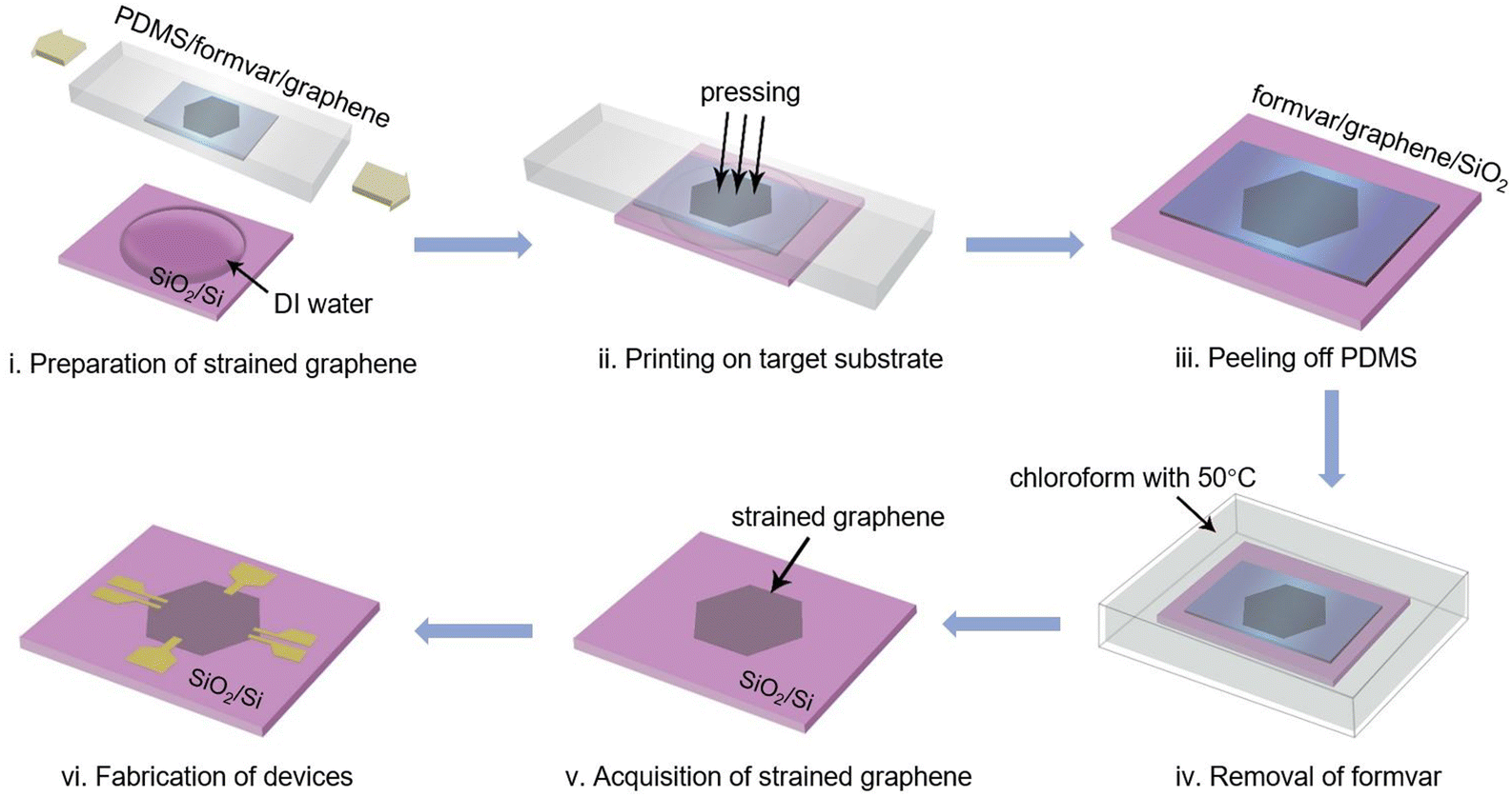 | ||
| Fig. 1 Schematic of the strain engineering of graphene on a rigid substrate of SiO2/Si, including the preparation of strained graphene using a flexible substrate, transfer printing of graphene onto the target substrate, peeling off the flexible substrate, removal of the protective layer, and post-processing steps. | ||
To characterize the quality of the strained graphene on the SiO2/Si substrate, multiple techniques were employed, as shown in Fig. 2. The graphene was synthesized as a single crystal using the chemical vapor deposition (CVD) method.20 The optical microscopy (OM) image in Fig. 2a shows that the strained graphene has high cleanness and flatness without any visible contaminations or wrinkles on its surface. The distinct hexagonal edges indicated by the black dotted lines demonstrate the high integrity of the graphene. The crack in the graphene is probably introduced by the peeling off of the PDMS layer considering that cracks can release the strain in graphene unless the graphene has already been in touch with the rigid substrate and its strain has already been fixed.21 The scanning electron microscopy (SEM) image in Fig. 2b proves that there were no obvious polymer residues on the graphene surface. Fig. 2c shows the atomic force microscopy (AFM) image of graphene within a 10 × 10 μm2 area and its height profile indicates that the maximum height variation in the graphene surface is about 2 nm, which is only about 16% of that for graphene transferred by polymethyl methacrylate (PMMA) (Fig. S3†). All the above results demonstrate that the strained graphene on the SiO2/Si substrate has high cleanness, flatness, and integrity, which are important for both fundamental research and the applications of graphene strain engineering.
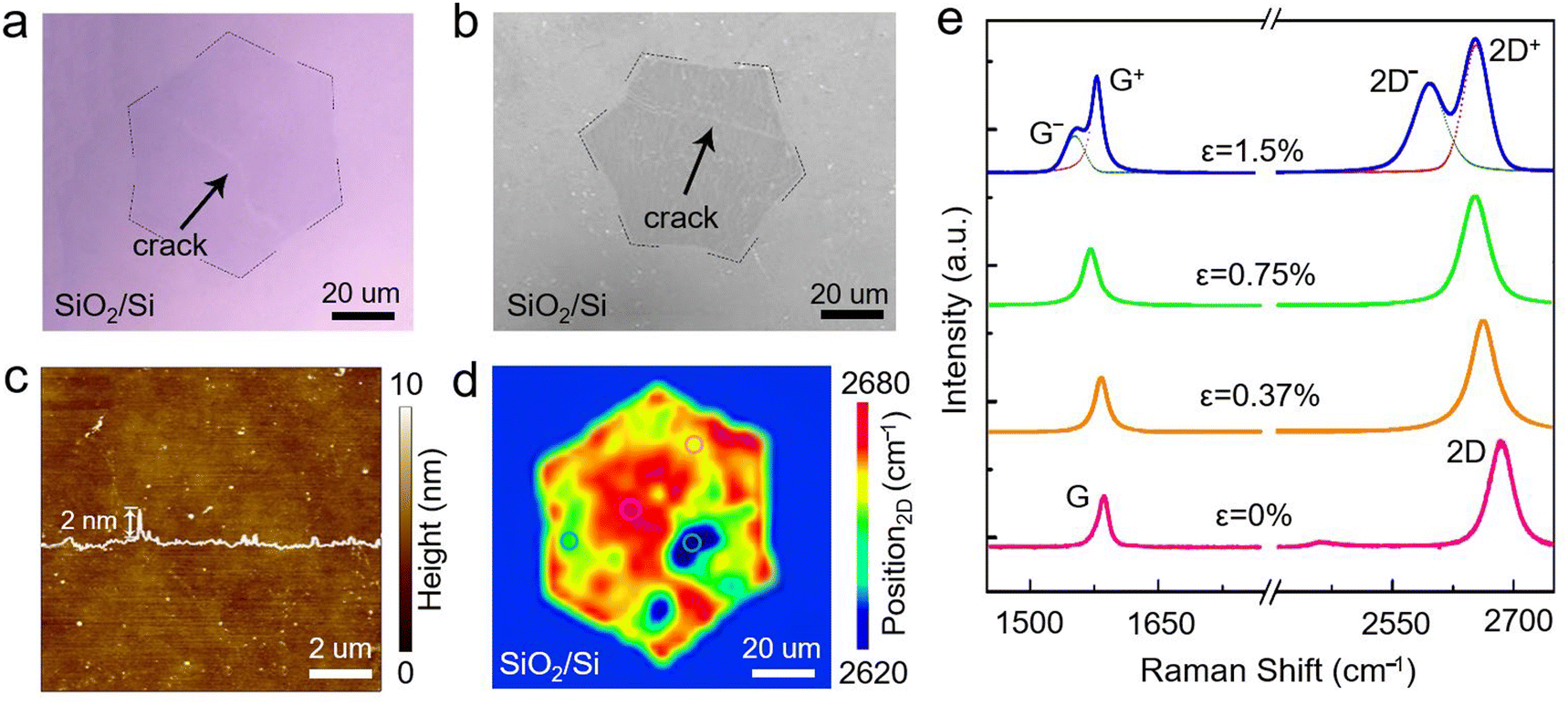 | ||
| Fig. 2 Characterizations of the strained graphene on SiO2/Si substrate. (a–c) OM, SEM and AFM images, respectively, of the strained graphene. The white line in 2c shows the height profile of the strained graphene. (d) Raman map of the 2D peak positions of the strained graphene. (e) Representative Raman spectra of graphene in circled regions in 2d. | ||
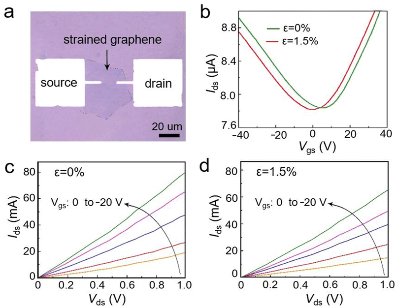 | ||
| Fig. 3 Electrical behaviours of strained graphene on SiO2/Si substrate. (a) OM image of fabricated graphene FET. Characteristic (b) transfer curves and (c and d) output curves of FETs fabricated with graphene with 0% and 1.5% strains, respectively. | ||
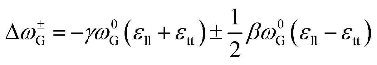
In order to evaluate the electronic and phonon structure changes as well as the quality of the strained graphene on the SiO2/Si substrate, non-destructive Raman spectroscopy was used. Fig. 2d shows the scanning Raman map of the 2D peak positions for strained graphene and the representative Raman spectra indicated by the coloured circles are shown in Fig. 2e. The scanning map was executed in a 100 × 100 μm2 area with a spatial resolution of 1 μm. To further characterize the quality of the strained graphene on the SiO2 substrate, we performed the scanned Raman spectra with an x-axis scale as shown in Fig. S4.† The results show that the intensity of the D peak (at about 1350 cm−1) representing defects is relatively low in the area away from the crack, confirming the high quality of the transferred graphene. As can been seen from the scanning Raman map, the graphene in the red region has a G peak (at about 1580 cm−1) and 2D peak (at about 2800 cm−1) that are close to the positions of transferred CVD graphene without any strain.22 However, for graphene in the regions indicated by other colours, the Raman peaks are shifted to lower wavenumbers. Particularly, for graphene in the blue region, its G and 2D peaks have each split into two subpeaks denoted by G−, G+, 2D− and 2D+, which results from the inconsistency of strain in the graphene along and perpendicular to the tensile direction.23 The G peak of graphene arises from the doubly degenerate E2g phonon mode at the Brillouin-zone centre and its split is caused by the loss of the six-fold and three-fold rotational symmetries of graphene under a uniaxial strain;16,23 the 2D peak redshifts under the synergy of the Dirac cone shifting and the anisotropic phonon softening at the same time.15,24 Note that the slightly larger strain values at the graphene edge are caused by a smoothing error from the Raman software, as shown in Fig. S5.† While Raman peak splitting for graphene strained by flexible substrates is commonly seen,25,26 this is the first time this splitting phenomenon has been observed on a rigid substrate.
The shift and splitting of the Raman peaks suggest that tensile uniaxial strains were successfully generated in graphene on the SiO2/Si substrate via the above procedures according to the well-established relation between graphene strain and its Raman peak:16
 | (1) |
We then characterized the electrical behaviors of strained graphene on SiO2/Si substrate by fabricating the back-gate graphene FETs as shown in Fig. 3a. For comparison, devices using unstretched graphene transferred by the same procedure without strain was also prepared, in both a 60 nm-thick nickel layer was evaporated on two sides of graphene as the source/drain electrodes. The transfer characteristic curves are shown in Fig. 3b, with Ids plotted as a function of Vgs at a fixed Vds. Both devices exhibit typical bipolar characteristic curves, indicating that the external electric field has made the type of carriers converted.25 However, with a maximum uniaxial strain of 1.4% in graphene, its energy bandgap has still not been opened. This is consistent with the prediction in other literatures that the strain threshold in graphene to open the energy bandgap is considerably large.26 In addition, the VDirac of FET fabricated by strained graphene is slightly left-shifted compared to that fabricated by graphene without strain, which in agreement with the result of strained graphene on flexible substrates.27,28
By decreasing Vgs from 0 to −20 V in a 5 V step, we further analyzed the output characteristic of graphene FETs with and without strain. As shown in Fig. 3c and d , the straight lines indicate good ohmic contact between electrodes and graphene. At the same Vds, the Ids measured from strained graphene FET is smaller than that of graphene without strain, implying that strain engineering causes a higher electrical resistance to graphene. This can be attributed to the symmetry break of graphene lattices under a uniaxial strain, which leads to a deformation of the electronic band structure and a change of the carrier concentration.25 Additionally, the low Ids at this condition proved that these devices have a small leakage current (Fig. S8†), which also demonstrates that the strained graphene on SiO2/Si substrate acquired by this method has a reliable electrical performance.
Finally, we discuss the key factors involved in this technique as shown in Fig. 4a. During the stretching process, the tensile graphene has undergone the asymmetric changes of lattices as mentioned above, which may dramatically reduce its high intrinsic fracture strength.29 When graphene was directly printed to the target substrate from the flexible stretching substrate, the effect of stress unloading can cause serious cracks to graphene under this asymmetric change. Therefore, a successful transfer printing requires a sufficient supporting strength to graphene to prevent the stress unloading.
As shown in the previous literature, formvar resin as a protective layer can supply graphene with an effective support during the transfer process.30 As shown by the comparative experimental result without formvar in Fig. 4b, the obtained graphene on the SiO2/Si substrate is destroyed disastrously. Fig. 4c shows the transfer printing result without a buffering liquid on target substrate. Obviously, only a small part of original graphene was left on the SiO2/Si substrate. It suggests that the buffering liquid dropped on the target substrate has a downwards capillary force to pull graphene/formvar stack to the target substrate, similar to our and other previous reported literatures.31,32 Therefore, it is reasonable to infer that the physical properties of the buffering liquid will strongly affect the preservation of graphene strain during the transfer printing process.
As can been seen from Fig. 4d, compared with heptane and ethanol as buffer liquids, DI water provides the graphene with the largest and most uniform values of strain. Several trials were performed and the results are summarized in Fig. 4e. The histogram shows that the maximum strain of graphene using DI water is about 1.5%, while those using ethanol and heptane are only approximately 0.5% and 0.25%, respectively, indicating that the use of DI water as the buffering liquid is robust and encouraging. We attribute this to the fact that the DI water, with a large contact angle on the graphene surface, can effectively fill the gap between the graphene and the adjacent interfaces of formvar and SiO2/Si substrate, as illustrated in Fig. 4a.35
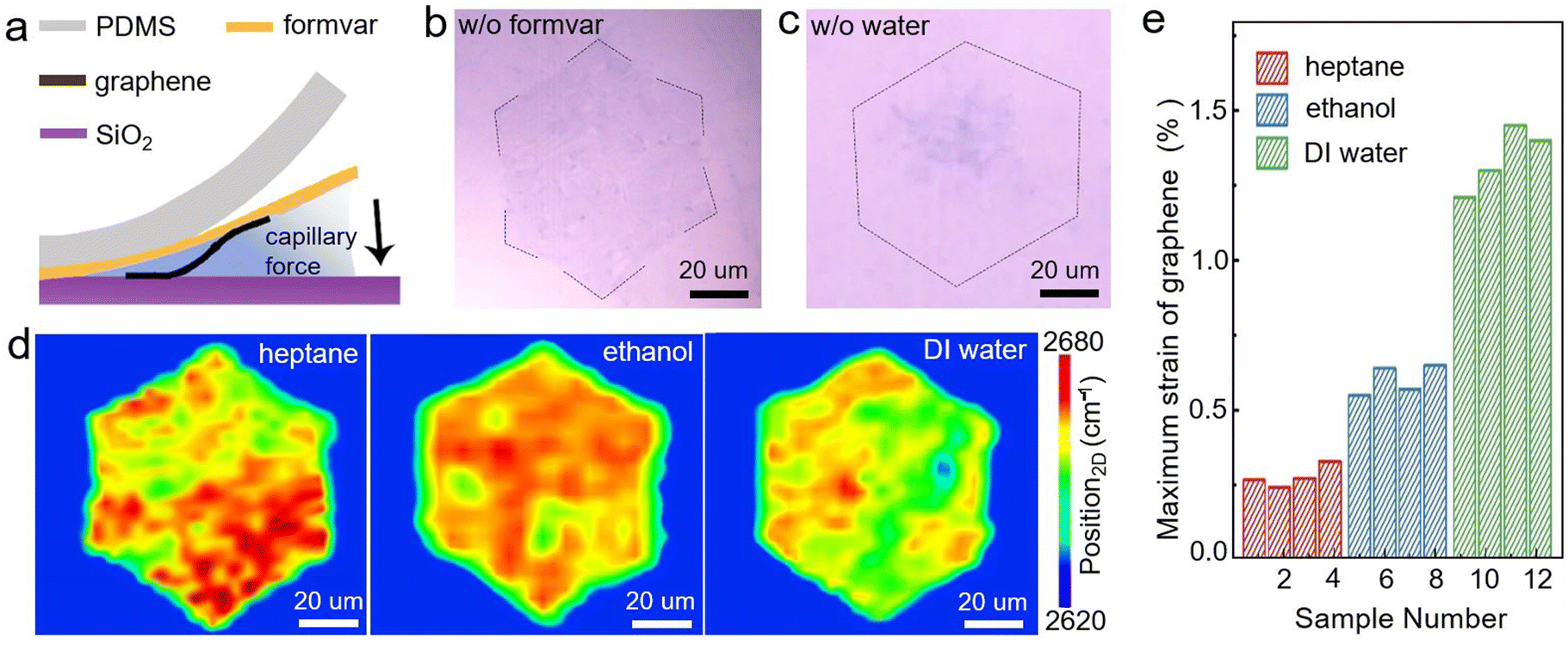 | ||
| Fig. 4 Key factors involved in this technique. (a) Illustration of the transfer printing method of strained graphene. (b and c) Transfer printing results of strained graphene without formvar and water, respectively. (d) Raman maps of 2D peak position and (e) maximum strain of strained graphene obtained by different buffering liquids. | ||
Additionally, the reason that graphene does not relax after being transferred onto the SiO2/Si substrate is the ultra-strong adhesion between graphene and the substrate, as well as the ‘downwards capillary force’ supplied by the buffering liquid. As demonstrated by previous works, the adhesion energy between graphene and the SiO2 surface is as strong as 0.45 ± 0.02 J m−2, which is reasonable for maintaining a 1.5% strain in graphene, considering that 2.5% and 3% strain values can be maintained by PDMS and epoxy with adhesion energies of only 0.4 and 0.42 J m−2, respectively.13,24,34,36,37 Furthermore, the buffering liquid on the SiO2/Si substrate supplies a downwards capillary force to further increase the adhesion energy between graphene and the SiO2/Si substrate, as demonstrated by the results in Fig. 4c and in previously published work.33,34,38 Theoretically, this can be extended to other 2D materials such as hBN and MoS2 and is also compatible with the strain engineering of 2D heterojunctions.
Conclusions
In conclusion, we have developed a novel and facile technique for graphene strain engineering on a rigid substrate. The maximum strain realized in graphene is about 1.5% and the strained graphene has high cleanness and integrity without apparent ripples. The FETs fabricated with the strained graphene demonstrate reliable electrical performances without an opened energy bandgap. The success of such strain engineering is attributed to the protection of the reinforcement layer of formvar resin and the capillary force of the buffering liquid DI water. We believe that this technique is also compatible with other 2D materials and can promote more development of strain engineering technologies on rigid substrates.Author contributions
Y. Z. and Y. J. initiated the research and conducted the experiments. J. L. and Q. R. prepared the samples. Z. C. and Y. Z. carried out characterizations of FET. P. Z. guided and supervised the whole project. All authors commented on the manuscript.Conflicts of interest
There are no conflicts to declare.Acknowledgements
This work was financially supported by the National Natural Science Foundation of China (11872330), Zhejiang Provincial Natural Science Foundation (R22A028805), and the Fundamental Research Funds for the Central Universities (226-2022-00172).References
- K. I. Bolotin, K. J. Sikes, Z. Jiang, M. Klima, G. Fudenberg, J. Hone, P. Kim and H. L. Stormer, Solid State Commun., 2008, 146, 351–355 CrossRef.
- A. A. Balandin, S. Ghosh, W. Z. Bao, I. Calizo, D. Teweldebrhan, F. Miao and C. N. Lau, Nano Lett., 2008, 8, 902–907 CrossRef PubMed.
- C. Lee, X. Wei, J. W. Kysar and J. Hone, Science, 2008, 321, 385–388 CrossRef PubMed.
- D. Zhan, J. Yan, L. Lai, Z. Ni, L. Liu and Z. Shen, Adv. Mater., 2012, 24, 4055–4069 CrossRef PubMed.
- G. G. Naumis and P. Roman-Taboada, Phys. Rev. B: Condens. Matter Mater. Phys., 2014, 89, 241404 CrossRef.
- Z. H. Ni, T. Yu, Y. H. Lu, Y. Y. Wang, Y. P. Feng and Z. X. Shen, ACS Nano, 2008, 2, 2301–2305 CrossRef.
- D. H. Kang, H. Sun, M. Luo, K. Lu, M. Chen, Y. Kim, Y. Jung, X. Gao, S. J. Parluhutan, J. Ge, S. W. Koh, D. Giovanni, T. C. Sum, Q. J. Wang, H. Li and D. Nam, Nat. Commun., 2021, 12, 5087 CrossRef.
- V. M. Pereira, A. H. Castro Neto and N. M. R. Peres, Phys. Rev. B, 2009, 80 Search PubMed.
- K. S. Novoselov, V. I. Fal'ko, L. Colombo, P. R. Gellert, M. G. Schwab and K. Kim, Nature, 2012, 490, 192–200 CrossRef CAS PubMed.
- K. S. Kim, Y. Zhao, H. Jang, S. Y. Lee, J. M. Kim, K. S. Kim, J. H. Ahn, P. Kim, J. Y. Choi and B. H. Hong, Nature, 2009, 457, 706–710 CrossRef CAS.
- Y. Shao, M. F. El-Kady, L. J. Wang, Q. Zhang, Y. Li, H. Wang, M. F. Mousavi and R. B. Kaner, Chem. Soc. Rev., 2015, 44, 3639–3665 RSC.
- P. Nemes-Incze, G. Kukucska, J. Koltai, J. Kurti, C. Hwang, L. Tapaszto and L. P. Biro, Sci. Rep., 2017, 7, 3035 CrossRef.
- S. P. Koenig, N. G. Boddeti, M. L. Dunn and J. S. Bunch, Nat. Nanotechnol., 2011, 6, 543–546 CrossRef CAS.
- C. Androulidakis, G. Tsoukleri, N. Koutroumanis, G. Gkikas, P. Pappas, J. Parthenios, K. Papagelis and C. Galiotis, Carbon, 2015, 81, 322–328 CrossRef CAS.
- D. Yoon, Y. W. Son and H. Cheong, Phys. Rev. Lett., 2011, 106, 155502 CrossRef.
- T. M. G. Mohiuddin, A. Lombardo, R. R. Nair, A. Bonetti, G. Savini, R. Jalil, N. Bonini, D. M. Basko, C. Galiotis, N. Marzari, K. S. Novoselov, A. K. Geim and A. C. Ferrari, Phys. Rev. B, 2009, 79, 205433 CrossRef.
- C. Neumann, S. Reichardt, P. Venezuela, M. Drogeler, L. Banszerus, M. Schmitz, K. Watanabe, T. Taniguchi, F. Mauri, B. Beschoten, S. V. Rotkin and C. Stampfer, Nat. Commun., 2015, 6, 8429 CrossRef CAS.
- J. Zabel, R. R. Nair, A. Ott, T. Georgiou, A. K. Geim, K. S. Novoselov and C. Casiraghi, Nano Lett., 2012, 12, 617–621 CrossRef CAS.
- Y. Jin, Q. Ren, J. Liu, Y. Zhang, H. Zheng and P. Zhao, Exp. Mech., 2022, 62, 761–767 CrossRef CAS.
- Y. Wang, Y. Cheng, Y. Wang, S. Zhang, X. Zhang, S. Yin, M. Wang, Y. Xia, Q. Li, P. Zhao and H. Wang, RSC Adv., 2018, 8, 8800–8804 RSC.
- P. R. Budarapu, B. Javvaji, V. K. Sutrakar, D. Roy Mahapatra, G. Zi and T. Rabczuk, J. Appl. Phys., 2015, 118 Search PubMed.
- W. S. Leong, H. Z. Wang, J. J. Yeo, F. J. Martin-Martinez, A. Zubair, P. C. Shen, Y. W. Mao, T. Palacios, M. J. Buehler, J. Y. Hong and J. Kong, Nat. Commun., 2019, 10, 1–8 CrossRef.
- M. Y. Huang, H. G. Yan, C. Y. Chen, D. H. Song, T. F. Heinz and J. Hone, Proc. Natl. Acad. Sci. U.S.A., 2009, 106, 7304–7308 CrossRef CAS PubMed.
- M. Huang, H. Yan, T. F. Heinz and J. Hone, Nano Lett., 2010, 10, 4074–4079 CrossRef CAS.
- L. Gong, I. A. Kinloch, R. J. Young, I. Riaz, R. Jalil and K. S. Novoselov, Adv. Mater., 2010, 22, 2694–2697 CrossRef CAS PubMed.
- T. Jiang, R. Huang and Y. Zhu, Adv. Funct. Mater., 2014, 24, 396–402 CrossRef CAS.
- J. Dong, S. Liu, Y. Fu and Q. Wang, Phys. Lett. A, 2017, 381, 292–297 CrossRef CAS.
- S.-M. Choi, S.-H. Jhi and Y.-W. Son, Phys. Rev. B, 2010, 81 Search PubMed.
- G. Hu, J. Wu, C. Ma, Z. Liang, W. Liu, M. Liu, J. Z. Wu and C.-L. Jia, Mater. Horiz., 2019, 6, 302–310 RSC.
- I. Gablech, J. Brodský, P. Vyroubal, J. Piastek, M. Bartošík and J. Pekárek, J. Mater. Sci., 2022, 57, 1923–1935 CrossRef.
- P. Zhang, L. Ma, F. Fan, Z. Zeng, C. Peng, P. E. Loya, Z. Liu, Y. Gong, J. Zhang, X. Zhang, P. M. Ajayan, T. Zhu and J. Lou, Nat. Commun., 2014, 5, 3782 CrossRef CAS PubMed.
- E. Auchter, J. Marquez, S. L. Yarbro and E. Dervishi, AIP Adv., 2017, 7, 125306 CrossRef.
- Y. Zhang, X. Zhang, Q. Ren, J. Liu, Z. Chen, M. Ma, L. Fan, Y. Zhao and P. Zhao, ACS Appl. Mater. Interfaces, 2022, 14, 14513–14519 CrossRef.
- Y. Hou, X. Ren, J. Fan, G. Wang, Z. Dai, C. Jin, W. Wang, Y. Zhu, S. Zhang, L. Liu and Z. Zhang, ACS Appl. Mater. Interfaces, 2020, 12, 40958–40967 CrossRef.
- F. Taherian, V. Marcon, N. F. A. van der Vegt and F. Leroy, Langmuir, 2013, 29, 1457–1465 CrossRef.
- C. C. Xu, T. H. Yang, Y. L. Kang, Q. Y. Li, T. Xue, K. M. Liechti, R. Huang and W. Qiu, Adv. Mater. Interfac., 2019, 6, 10 Search PubMed.
- T. Yoon, W. C. Shin, T. Y. Kim, J. H. Mun, T.-S. Kim and B. J. Cho, Nano Lett., 2012, 12, 1448–1452 CrossRef CAS.
- X. Ma, Q. Liu, D. Xu, Y. Zhu, S. Kim, Y. Cui, L. Zhong and M. Liu, Nano Lett., 2017, 17, 6961–6967 CrossRef CAS.
Footnote |
| † Electronic supplementary information (ESI) available. See DOI: https://doi.org/10.1039/d2na00580h |
| This journal is © The Royal Society of Chemistry 2022 |