
 Open Access Article
 This Open Access Article is licensed under a Creative Commons Attribution-Non Commercial 3.0 Unported Licence
Uniform self-rectifying resistive random-access memory based on an MXene-TiO2 Schottky junction†
Chao
Zang‡
ab,
Bo
Li‡
ab,
Yun
Sun
*ab,
Shun
Feng
ac,
Xin-Zhe
Wang
ab,
Xiaohui
Wang
 *ab and
Dong-Ming
Sun
*ab
*ab and
Dong-Ming
Sun
*ab
aShenyang National Laboratory for Materials Science, Institute of Metal Research, Chinese Academy of Sciences, 72 Wenhua Road, Shenyang, 110016, China. E-mail: yunsun@imr.ac.cn; wang@imr.ac.cn; dmsun@imr.ac.cn
bSchool of Materials Science and Engineering, University of Science and Technology of China, 72 Wenhua Road, Shenyang, 110016, China
cSchool of Physical Science and Technology, ShanghaiTech University, 393 Huaxiazhong Road, Shanghai, 200031, China
First published on 11th October 2022
Abstract
For filamentary resistive random-access memory (RRAM) devices, the switching behavior between different resistance states usually occurs abruptly, while the random formation of conductive filaments usually results in large fluctuations in resistance states, leading to poor uniformity. Schottky barrier modulation enables resistive switching through charge trapping/de-trapping at the top-electrode/oxide interface, which is effective for improving the uniformity of RRAM devices. Here, we report a uniform RRAM device based on a MXene-TiO2 Schottky junction. The defect traps within the MXene formed during its fabricating process can trap and release the charges at the MXene–TiO2 interface to modulate the Schottky barrier for the resistive switching behavior. Our devices exhibit excellent current on-off ratio uniformity, device-to-device reproducibility, long-term retention, and endurance reliability. Due to the different carrier-blocking abilities of the MXene–TiO2 and TiO2–Si interface barriers, a self-rectifying behavior can be obtained with a rectifying ratio of 103, which offers great potential for large-scale RRAM applications based on MXene materials.
Introduction
Metal oxide junctions are one of the most fundamental building blocks for practical electronic devices.1–3A Schottky barrier is formed at the metal–oxide interface due to the difference between metal work function and oxide electron affinity.4 Recently, resistive random-access memory (RRAM) devices based on metal oxide junctions have been increasingly recognized as a mainstream technology to meet the requirements of the rapid development of non-volatile data storage,5–11 logic operation12 and neural computing13–16 due to their simple configuration, and high reproducibility.11,17,18However, due to the stochastic nature of the filamentary resistive switching mechanism, the inevitable variability should be a primary obstacle for RRAMs.19,20 Theoretically, conductive filaments across the junction can be formed/ruptured by the redox process,21 migration of oxygen vacancies,11,22 or diffusion of atoms/ions of active metal electrodes,23 depending on the various metal oxide junctions.19,24–26 Nevertheless, switching between different resistance states is usually abrupt, and the random formation of conductive filaments usually makes large fluctuations of both resistance state and operating voltage, which greatly weakens the reliability of memory devices, and will either falsely program/erase the storage cell or make the storage states unrecognizable, imposing challenges to the peripheral sensing and programming circuits.19 Therefore, seeking a resistive switching mechanism that could eliminate the involvement of the prominent local conductive filamentary is impending for the development of uniform RRAM devices.
Another acknowledged resistive switching mechanism is the field-induced modulation of the Schottky barrier profile, which usually occurs on the entire interface between the electrode and oxide to improve the uniformity. It is well accepted that the interface state seriously affects the formation of the Schottky barrier, and the field-induced modification of the interface state contributes to the memory effect.27 The charge carriers injected from the electrodes may be trapped by charge traps in a storage medium to form a space charge, which can either modulate the barriers to injection of the charge carriers from the electrodes or affect the transport process of charge carriers through the storage medium, thereby leading to the resistive switching behavior.25 Furthermore, by inducing a Schottky contact or asymmetric barrier into a charge trapping/detrapping system, a charge-trap-associated self-rectifying RRAM can be obtained to deal with the sneak path problem that leads to the misreading, false program and additional power consumption in a high-density, massively parallel crossbar array.28–31 Therefore, designing a Schottky junction with abundant charge traps within the metal-oxide interface should be feasible to fabricate uniform self-rectifying RRAM devices.
MXenes are a new class of transition metal carbides or nitrides, which are widely used in electronic devices as electrode materials due to their excellent metallic conductivity and good hydrophilicity.32,33 It is worth noting that during the preparation of MXenes, when a certain A atomic layer is removed from the MAX phase precursor by hydrofluoric acid etching, some adjacent atoms will inevitably fall off, leading to the disordered anion–cation vacancies or vacancy clusters, which greatly increase the trap density of MXenes inherently.34–36 Recently, as the wafer-scale MXene film patterning with high resolution has been realized,37 it opens up new avenues for designing highly-active and long-life electrode candidates for fabricating uniform RRAMs based on the interface-trap modulation model.
Here, we report a uniform RRAM device with the MXene-TiO2 Schottky junction, while MXene and TiO2 are used as the top-electrode and resistive layer, respectively. The resistive switching behavior comes from the MXene-TiO2 junction, where the barrier profile is electrically modulated. The charge carriers injected from the MXene top-electrode can be trapped by charge traps within the MXene-TiO2 interface to modulate the barriers. As a result, our device exhibits the uniformity of current on–off ratio with a standard deviation less than 0.25, device-to-device reproducibility, long-term retention of 104 s, and reliable endurance. Moreover, by introducing the bottom electrode with silicon, a self-rectifying behavior can be obtained with a rectifying ratio of 103 due to the different carrier-blocking abilities of the MXene-TiO2 and TiO2–Si interface barrier.
Results and discussions
Device design and characterization
Fig. 1a shows the schematic of a RRAM comprised of a MXene top-electrode, TiO2 resistive layer and p+-Si bottom-electrode. The fabricated device features an effective electrode junction area of 10 μm × 10 μm, which is denoted by white dash lines in Fig. 1b. Fig. 1c shows an AFM image of the morphology of the deposited uniform MXene film with 25 nm as the top-electrodes according to the height profile (ESI Fig. S1†).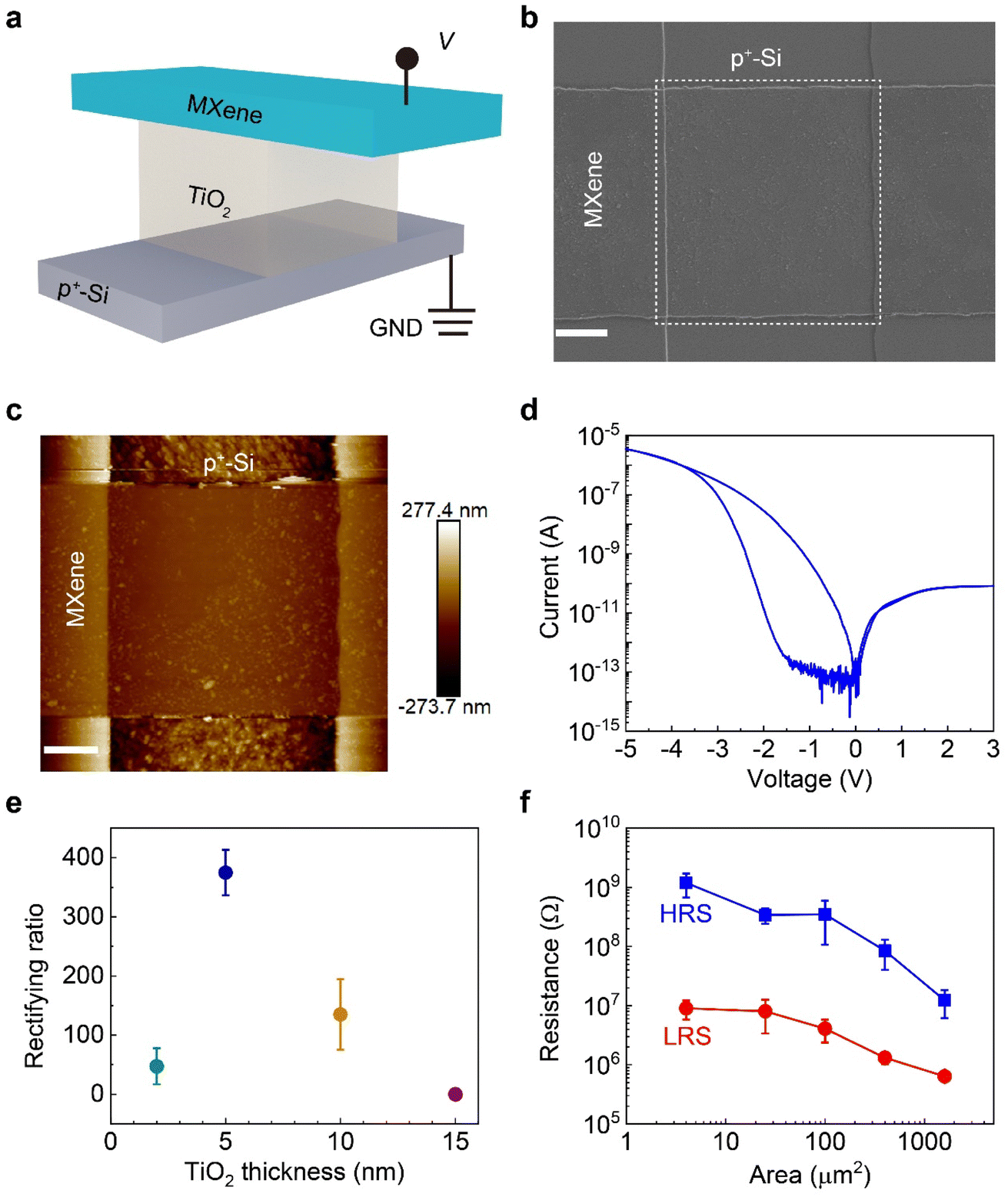 | ||
| Fig. 1 Device design and characterization. (a) Schematic of a MXene-TiO2-Si RRAM. (b) SEM image of the crossbar structure with a resistive area of 10 μm × 10 μm denoted by white dash lines. Scale bar, 3 μm. (c) AFM image of the morphology of a 25 nm-thick MXene film. Scale bar, 2 μm. (d) Typical I–V characteristic of a MXene-TiO2-Si RRAM indicates the self-rectifying switching behavior. (e) Rectifying ratio of the RRAMs as a function of various TiO2 thicknesses, calculated from the I–V characteristics of 5 devices for each TiO2 thickness. (f) Relationship of the resistive area and the performance of MXene-TiO2-Si self-rectifying RRAMs, extracted from the I–V characteristics of 10 devices for each resistive area. | ||
A typically measured current–voltage (I–V) characteristic of the device shows that the self-rectifying behaviors are realized successfully with a rectifying ratio of approximately 103 (Fig. 1d). During the SET process, when the SET voltage (VSET) is approximately −2 V, the conduction of the resistive layer changes from a high-resistance state (HRS) to a low-resistance state (LRS), thereby switching the device to the ON state. During the RESET process, a RESET voltage (VRESET) of 2 V is applied to “erase” the device and causing it to return to the OFF state, with the conduction of the resistive layer changing from the LRS to the HRS, where the current is evidently suppressed. The rectifying ratio is calculated by the currents at −2 V and 2 V (ESI Fig. S2†). It is also appropriate to set the read voltage of ±2 V due to the stable read disturbance for HRS and LRS with a current on–off ratio of approximately 102 (ESI Fig. S3†).
To determine the appropriate device structure, a comparison of RRAM switching behaviors with different thicknesses of TiO2 as the resistive layer has been carried out, as shown in Fig. 1e, indicating that the optimum thickness of the TiO2 resistive layer is 5 nm. As a matter of fact, at the ON state, a thinner TiO2 film can result in the tunneling of charge carriers under the bias voltage, while a thicker TiO2 film can be considered as a good dielectric to impede the conduction between the top and bottom electrodes completely without any resistive switching behaviors (ESI Fig. S4†). An appropriate thickness is helpful for the construction of devices with a better rectifying ratio.38,39 In our study, as the TiO2 thickness increases, the Schottky barrier height and contact resistance can be reduced; however, the thicker TiO2 has a larger series resistance leading to the degradation of device performance at the contact.40 As a result, 5 nm-TiO2 should be just appropriate for obtaining the largest rectifying ratio by balancing the effects on the Schottky barrier height and series resistance simultaneously.
Fig. 1f shows the relationship between the resistive area and the performance of RRAMs extracted from the I–V characteristics of 10 devices each with different geometries (ESI Fig. S5†). Note that both the resistance of HRS and LRS decrease with the increased resistive area. Such an area-sensitive characteristic of the resistance states confirms the field-induced modulation of the Schottky barrier profile occurred on the entire MXene–TiO2 interface.4 In addition, the current of our devices with the smallest resistive area is more than 2 nA, which is big enough to read. In the practical chip design, even the current of fA level can be collected by adding auxiliary circuits, such as operational amplifiers.41–43
To verify the Schottky junction between MXene and TiO2, we directly connect two probes with MXene and TiO2, respectively (Fig. 2a). As a result, there is no rectifying behavior obtained in the case of either MXene or TiO2 connected with two probes. We directly measure the I–V characteristic of the TiO2–Si junction with a typical diode behavior (ESI Fig. S6†). When the MXene–TiO2 junction is tested, one probe is connected with the MXene and the other is connected with TiO2. Consequently, an obvious rectifying behavior is obtained, and we deduced that a Schottky junction is formed between MXene and TiO2 as a metal–semiconductor contact. Furthermore, several RRAMs using different metal materials as the top-electrodes have been fabricated to explore the importance of MXene, including Al, Ti and Au. As a result, no matter what kind of the metal top electrode is, no resistive switching behavior is observed for these RRAM devices (Fig. 2b) due to the lack of sufficient traps within the metal–TiO2 interface.44,45 Therefore, we clarify that the intrinsic traps of MXenes play an essential role in the switching of the resistance flow process.46–49
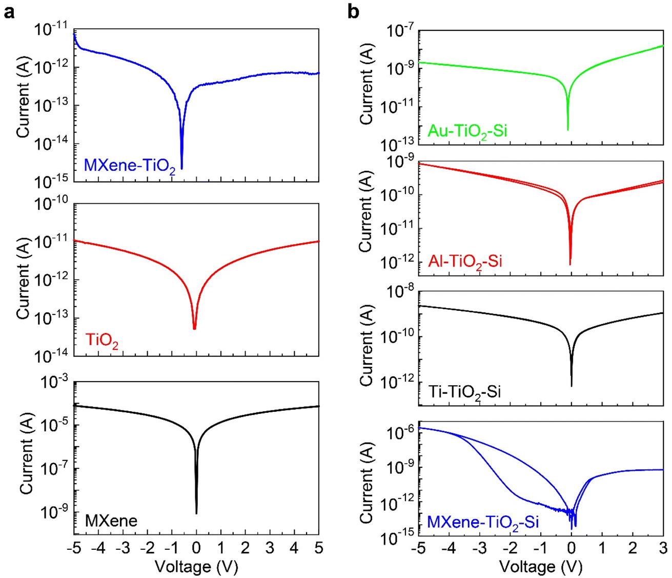 | ||
| Fig. 2 a) I–V characteristics of the MXene–TiO2 junctions, TiO2 and MXene films. (b) Performance comparison of the RRAMs with various top-electrodes including Au, Al and Ti and MXene. The resistive area and the performance of MXene-TiO2-Si self-rectifying RRAMs, extracted from the I–V characteristics of 10 devices for each resistive area. | ||
Switching retention and endurance are critical to evaluate the reliability of RRAM devices. As shown in Fig. 3a, the retention characteristics of the MXene-TiO2-Si RRAM show that the HRS is not significantly degraded after 104 s, but the LRS increases slightly. This is because the modulation of the Schottky barrier at the HRS is stable and easily realized. However, for the LRS, it suggests that some electrons may be injected from the MXene electrode and occupied the charge traps entering the interface. As a result, some positive charge traps are neutralized and the Schottky barrier within the interface is recovered leading to a slight increase in resistance. Moreover, the endurance characteristics show a stable operation of 100 cycles (Fig. 3b). Actually, our RRAM device could be also maintained beyond 100 cycles depending on how to set the pulsed voltage stress (ESI Fig. S7†). In addition, to predict the lifetime of our RRAM devices, we have investigated the retention and endurance characteristics at different temperatures (ESI Fig. S8†). It is explicit that the stable retention and recognizable on/off behaviors are still maintained. According to the Arrhenius equation, the activation value Ea of our device is calculated as 1.78 eV, and the extrapolated retention time of our device at room temperature could be approximately 108 s (ESI Fig. S9†), which is estimated by temperature-dependence of the retention time following the Arrhenius equation. In fact, there is little degradation of LRS at a higher temperature. This is because the stability of LRS is related to the activation energy of the material, and the greater the activation energy, the poorer the thermal stability of LRS.50 In addition, compared with some thermal-stability RRAM devices,51,52 the Ea of our RRAM device is a little larger leading to the degradation of LRS at a higher temperature. All these results can prove the high reliability of the MXene-TiO2-Si RRAM devices for long-term data storage.49
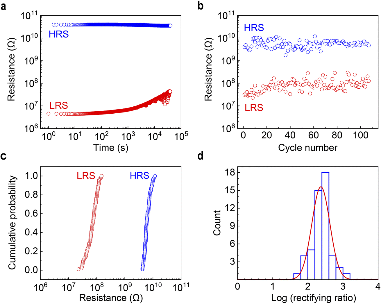 | ||
| Fig. 3 Evaluation of the electrical performance. (a) Retention and (b) endurance characteristics of the MXene-TiO2-Si RRAM obtained at ±2 V and the room temperature. (c) Device-to-device cumulative probability of 100 individual MXene-TiO2-Si RRAMs based on the resistance of HRS and LRS. (d) Statistical distribution of rectifying ratio of 50 MXene-TiO2-Si RRAMs with a standard deviation of 0.25. | ||
Fig. 3c shows the cumulative probability of 100 individual MXene-TiO2-Si RRAMs based on the resistance of HRS and LRS with a device-to-device variation less than one order of magnitude indicating the good uniformity. Fig. 3d illustrates the statistical distribution of rectifying ratio extracted from 50 individual RRAMs (ESI Fig. S10†). Due to the logarithmic operation, the mean rectifying ratio is actually 4 × 10² with a standard deviation of approximately 0.25. Moreover, we also provide the I–V characteristics of a RRAM with 80 switching cycles ((ESI Fig. S11†) and plot the statistical variation of rectifying ratio from cycle-to-cycle. As a result, the rectifying ratio only distributed from 102 to 103, indicating the excellent cycle-to-cycle uniformity (ESI Fig. S12†). The narrow distribution of switching voltages and resistance states illustrates the robust programming/erasing of the memory or making the storage states recognizable. Similarly, even though the bottom electrode is replaced by n-Si, the self-rectifying behavior and retention characteristics of the MXene-TiO2-n-Si are also achieved, indicating the excellent reliability and stability of MXene–TiO2 Schottky junction for fabricating the uniform self-rectifying RRAM devices (ESI Fig. S13†). All of these critical metrics can compare favourably with the reported TiO2-based RRAMs23,26,49,53–56 (ESI Table S1†).
Mechanism
The proposed mechanism of MXene-TiO2-Si RRAM about the resistive switching and self-rectifying behaviors is elucidated. Theoretically, in the interface-type charge trapping/de-trapping mechanism, there are charge traps at the interface of the Schottky junction, and the trapping and de-trapping of charges can modulate the height of the Schottky barrier to induce the resistance transition.19–23,53 In addition, the occupied state of the charge traps is affected by the carriers injected from the electrodes.17 A reverse bias voltage relative to the Schottky barrier causes the trapped charges and increases the interface resistance, while a forward bias voltage makes the interface traps to release the trapped charges, thereby decreasing the interface resistance.25–27As shown in Fig. 4a, when a relatively large negative bias is applied to the Schottky interface, electrons are extracted from the defect, resulting in the accumulation of positive charge traps at the interface, which changes the distribution of the potential at the interface. In order to maintain the suppression of the Fermi level position between MXene and TiO2, the height of the Schottky barrier at the interface is reduced leading to the decrease of the interface contact resistance, while the device is transformed into LRS; however, when a large positive bias is applied, a large number of electrons are injected into the interface and fill the charge traps, thereby neutralizing these positive charge traps and restoring the interface Schottky barrier, while the device transitions back to HRS.56–59
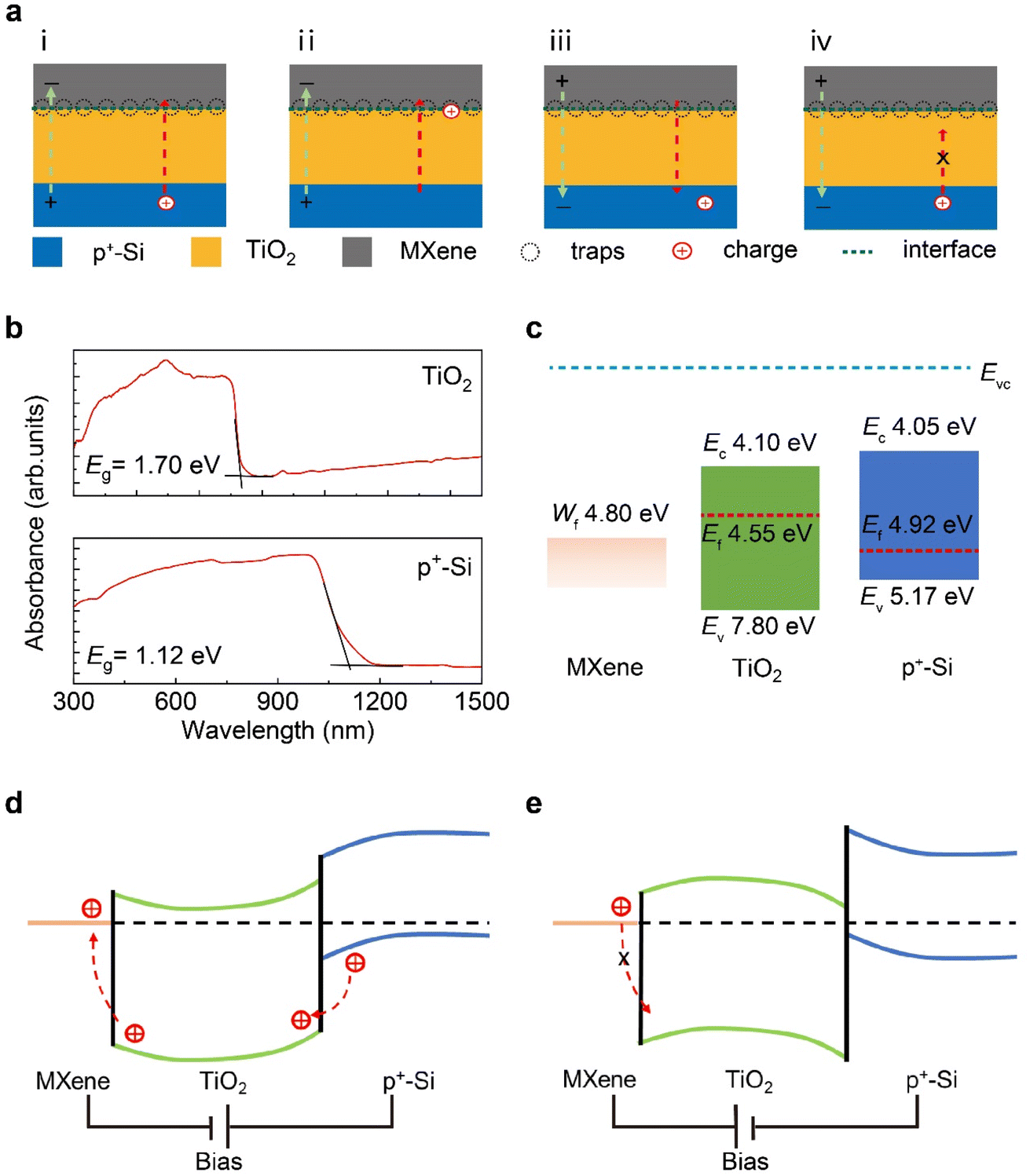 | ||
| Fig. 4 Mechanism. (a) Resistive switching of the MXene-TiO2-Si RRAM device (i. V = VSET, ii. Trap, iii. Detrap, iv. V = VRESET). (b) Absorbance spectrum of TiO2 and p+-Si. Eg is the bandgap. The red line is an auxiliary line for extracting Eg. (c) Energy band diagram of MXene, TiO2 and p+-Si. Band diagram of the MXene-TiO2-Si heterojunction under (d) negative and (e) positive bias. | ||
Fig. 4b shows the absorbance spectra, which demonstrate the bandgaps of TiO2 and p+-Si are 1.70 eV and 1.12 eV, respectively. Therefore, the self-rectification of the device is approved based on the basic energy band structure of each material (Fig. 4c), which is drawn through their work function and other parameters (ESI Fig. S14†).
When the device is negatively biased (Fig. 4d), it is easier for carriers to cross the Schottky barrier between MXene and TiO2, allowing more current to flow through the device in the ON state. Conversely, when the device is positively biased (Fig. 4e), it is difficult for carriers to pass through the Schottky barrier between MXene and TiO2 due to the different carrier-blocking abilities of the MXene–TiO2 and TiO2–Si interface barrier, resulting in the device self-rectifying behavior.60
In the case of n-Si, when n-Si contacts with MXene to form a Schottky junction, the holes as primary carriers cause the opposite built-in electric field inside this junction compared with p-Si. Therefore, under the same bias voltage, the voltage has the opposite effect on the device switching behavior.
Conclusions
We report a new design method to fabricate uniform self-rectifying RRAM devices with a rectifying ratio of approximately 103 based on the MXene–TiO2 Schottky junction. The defect traps within MXene formed spontaneously during its preparation process play an essential role in the modulation of the Schottky barrier by charge trapping/de-trapping as a storage medium at the entire MXene–TiO2 interface. Our devices exhibit the excellent uniformity, device-to-device reproducibility, long-term retention, and reliability, which paves a new path for the fabrication of large-scale memory devices based on MXene materials.Material preparation
The MXene used for the top electrodes comes from a colloidal Ti3C2Tx solution. First, Ti3AlC2 powder (2 g) synthesized using a high-temperature solid–liquid reaction was slowly added to an HCl solution (40 mL, 9 M) with LiF (2 g), preparing a Ti3C2Tx suspension. Then, Ti3C2Tx slurry was obtained by vacuum filtration and cleaned by deionized (DI) water until pH reaches 5, while the Ti3C2Tx suspension was poured onto a porous filter membrane after the solution stops bubbling. At last, a colloidal Ti3C2Tx solution was obtained after sonication of the Ti3C2Tx slurry diluted with DI water for 30 min.Other chemicals used include remover PG (MicroChem), CD-26 developer (MicroChem), acetone, isopropanol and ethanol. All chemicals were directly used without any further purification.
Fabrication of RRAM device
In a typical preparation, a heavily doped p+-Si substrate with 100 nm SiO2 (Silicon Quest International, Inc.) was firstly cleaned with acetone and isopropanol for 5 min each, followed by purging with nitrogen gas. The cleaned substrate was then patterned by standard photolithography and etched by reactive ion etching (15 sccm Ar, 20 sccm CHF3, 20 sccm CF4) to remove the redundant SiO2 to expose p+-Si, and it was used as the bottom electrode. To improve the cleanliness of the substrate, the oxygen plasma treatment was further applied for 10 min at 200 W and O2 of 180 sccm. Subsequently, a 5 nm-thick TiO2 was deposited on the bottom electrodes by atomic layer deposition (ALD) at 250 °C (precursor: tetraisopropyl titanate, TTIP and H2O). According to the constant height profile and X-ray photoelectron spectroscopy of the structure of the bottom Si electrode before and after ALD, it is explicit that there is no redundant SiO2 at all within the TiO2–Si interface (ESI Fig. 15†). After that, MXene (Ti3C2Tx, 10 mg mL−1) was spin-coated at 2000 rpm for 1 min to prepare the uniform MXene thin-films for the top-electrodes. The patterned Al (60 nm) was then prepared on the MXene as the metal mask, and the redundant MXene outside the electrode area was removed by reactive ion etching at 4 Pa, 5 W and 20 sccm CF4 for 2.5 min. Finally, the Al metal mask was removed by immersing it into CD-26 developer for 2 min at room temperature, cleaned with DI water for 1 min, and then purged with nitrogen gas (ESI Fig. S16†).Characterization of material and device
The fabricated devices were characterized using an optical microscope (Nikon ECLIPSE LV100ND), a scanning electron microscope (SEM, FEI Nova NanoSEM430, acceleration voltage of 1 kV), and an atomic force microscope (AFM, Bruker Dimension Icon). A semiconductor analyzer (Agilent B1500A), a probe station (Cascade M150) and an input signal generator (Tektronix AFG 3022C) were used to measure the electrical performance under ambient conditions, including retention and endurance characteristics. An ultraviolet-visible-near infrared spectrometer (UV-VIS-NIR Spectrometer, UV3600 Plus) was used to measure the absorbance spectrum. A Kelvin probe force microscope (KPFM, MultiMode 8, Bruker, Inc.) was used to measure the work function.Author contributions
Y. S. and D. M. S conceived and designed the experiments. C. Z., Y. S. and B. L. performed the device fabrication, electrical characterization and the bandgap evaluation for the device mechanism. F. S. performed the SEM characterization of the device structure. X. Z. W performed the AFM characterization of MXene morphology. C. Z. performed the ALD of TiO2 for the resistive layer. X. H. W. prepared the MXene solution. Y. S. and D. M. S. co-wrote the paper. All authors discussed the results and commented on the manuscript.Conflicts of interest
There are no conflicts to declare.Acknowledgements
This work was supported by the National Key Research and Development Program of China (2021YFA1200801), the National Natural Science Foundation of China (62125406, 62074150, 52188101), the Strategic Priority Research Program of the Chinese Academy of Sciences (XDB30000000), the Key Research Program of Frontier Sciences of the Chinese Academy of Sciences (ZDBS-LY-JSC027).Notes and references
- S. M. Sze, Phys. Today, 1970, 23, 75 CrossRef.
- A. Zangwill and J. W. Gadzuk, Phys. Today, 1988, 100, 1463–1464 Search PubMed.
- K. G. Rana, V. Khikhlovskyi and T. Banerjee, Appl. Phys. Lett., 2012, 100, 213502 CrossRef.
- Z. B. Yan and J. M. Liu, Sci. Rep., 2013, 3, 2482 CrossRef CAS PubMed.
- Z. Yan, Y. Guo, G. Zhang and J. M. Liu, Adv. Mater., 2011, 23, 1351–1355 CrossRef CAS PubMed.
- D. S. Jeong, R. Thomas, R. S. Katiyar, J. F. Scott, A. Petraru and C. Seong, Rep. Prog. Phys., 2012, 75, 076502 CrossRef.
- Y. Hikita, M. Kawamura, C. Bell and H. Y. Hwang, Appl. Phys. Lett., 2011, 98, 192103 CrossRef.
- E. Lee, M. Gwon, D. K. Kim and H. Kim, Appl. Phys. Lett., 2011, 98, 132905 CrossRef.
- J. Sun, C. H. Jia, G. Q. Li and W. F. Zhang, Appl. Phys. Lett., 2012, 101, 133506 CrossRef.
- Z. Wen, C. Li C, D. Wu, A. Li and N. Ming, Nat. Mater., 2013, 12, 617–621 CrossRef CAS PubMed.
- J. J. Yang, M. D. Pickett, X. Li, D. A. A. Ohlberg, D. R. Stewart and R. S. Williams, Nat. Nanotechnol., 2008, 3, 429–433 CrossRef CAS.
- C. Liu, H. Chen, X. Hou, H. Zhang and P. Zhou, Nat. Nanotechnol., 2019, 14, 662 CrossRef CAS.
- Z. Wang, S. Ambrogio, S. Balatti and I. Daniele, Front. Neurosci., 2015, 8, 438 Search PubMed.
- F. Zhou, Z. Zhou, J. Chen, T. H. Choy and Y. Chai, Nat. Nanotechnol., 2019, 14, 776–782 CrossRef CAS PubMed.
- Z. Wang, T. Zeng, Y. Ren, Y. Lin and D. Ielmini, Nat. Commun., 2020, 11, 1150 CrossRef PubMed.
- W. Banerjee, Q. Liu, H. Lv, S. Long and M. Liu, Nanoscale, 2017, 9, 14442–14450 RSC.
- R. Waser and M. Aono, Nat. Mater., 2007, 6, 833 CrossRef CAS.
- Z. Wang, H. Wu, G. W. Burr, C. S. Hwang, K. L. Wang, Q. Xia and J. J. Yang, Nat. Rev. Mater., 2020, 5, 173–195 CrossRef CAS.
- Z. Zhang, Z. Wang, T. Shi, C. Bi and P. Zhou, InfoMat, 2020, 2, 261–290 CrossRef CAS.
- W. Banerjee, Electronics, 2020, 9, 1029 CrossRef CAS.
- R. Waser, R. Dittmann, G. Staikov and K. Szot, Adv. Mater., 2009, 21, 2632–2663 CrossRef CAS.
- X. Cao, X. M. Li, X. D. Gao, Y. W. Zhang, X. J. Liu, Q. Wang and L. D. Chen, Appl. Phys. A: Mater. Sci. Process. , 2009, 97, 883–887 CrossRef CAS.
- W. Banerjee, X. Xu, H. Lv, Q. Liu, S. Long and M. Liu, ACS Omega, 2017, 2, 6888–6895 CrossRef CAS PubMed.
- L. Qi, J. Sun, H. Lv, S. Long, K. Yin, N. Wan, Y. Li, L. Sun and M. Liu, Adv. Mater., 2012, 24, 1844–1849 CrossRef.
- F. Pan, S. Gao, C. Chen, C. Song and F. Zeng, Mater. Sci. Eng. R Rep., 2014, 4, 1–59 CrossRef.
- W. Banerjee and H. Hwang, Adv. Electron. Mater., 2020, 6, 2000488 CrossRef.
- X. G. Chen, X. B. Ma, Y. B. Yang, L. P. Chen, G. C. Xiong, G. J. Lian, Y. C. Yang and J. B. Yang, Appl. Phys. Lett., 2011, 98, 122102 CrossRef.
- C. Li, L. Han, H. Jiang, M. Jang, P. Lin, Q. Wu, M. Barnell, J. J. Yang, H. Xin and Q. Xia, Nat. Commun., 2017, 8, 15666 CrossRef CAS.
- L. Shi, G. Zheng, B. Tian, B. Dkhil and C. Duan, Nanoscale, 2020, 2, 1811–1827 RSC.
- J. H. Yoon, S. Yoo, S. J. Song, K. J. Yoon, D. E. Kwon, Y. J. Kwon, T. H. Park, H. J. Kim, X. L. Shao, Y. Kim and C. S. Hwang, ACS Appl. Mater. Interfaces, 2016, 8, 18215–18221 CrossRef CAS PubMed.
- J. H. Yoon, D. E. Kwon, Y. Kim, Y. J. Kwon, K. J. Yoon, T. H. Park, X. L. Shao and C. S. Hwang, Nanoscale, 2017, 9, 11920–11928 RSC.
- B. Lyu, M. Kim, H. Jing, J. Kang and J. H. Cho, ACS Nano, 2019, 13, 11392–11400 CrossRef CAS.
- Z. Lin, H. Shao, K. Xu, P. L. Taberna and P. Simon, TrAC, Trends Anal. Chem., 2020, 2, 654–664 CrossRef CAS.
- Y. Cui, Z. Cao, Y. Zhang, H. Chen, J. Gu, Z. Du, Y. Shi, B. Li and S. Yang, Small, 2021, 6, 2100017 CrossRef.
- T. Sun, G. Zhang, D. Xu, X. Lian, H. Li, W. Chen and C. Su, Mater. Today Energy, 2019, 12, 215–238 CrossRef.
- Y. Tang, C. Yang, X. Xu, Y. Kang, J. Henzie, W. Que and Y. Yamauchi, Adv. Energy Mater., 2022, 12, 2103867 CrossRef CAS.
- B. Li, Q. B. Zhu, C. Cui, Z. H. Wang, S. Feng, Y. Sun, H. Zhu, X. Su, Y. Zhao, H. Zhang, J. Yao, S. Qiu, Q. Li, X. Wang, X. Wang, H. Cheng and D. Sun, Adv. Mater., 2022, 34, 2201298 CrossRef CAS PubMed.
- A. K. Bilgili, R. Çağatay, M. K. Öztürk and M. Özer, Silicon, 2022, 14, 3013 CrossRef CAS.
- J. Kwon, J. Y. Lee, Y. J. Yu, C. H. Lee, X. Cui, J. Hone and G. H. Lee, Nanoscale, 2017, 9, 6151 RSC.
- G. S. Kim, S. W. Kim, S. H. Kim, J. Park, Y. Seo, B. J. Cho, C. Shin, J. H. Shim and H. Y. Yu, ACS Appl. Mater. Interfaces, 2016, 8, 35419 CrossRef CAS.
- J. Lu and J. Holleman, IEEE CICC, 2012, 1–4 CrossRef.
- P. Neužil, C. D. M. Campos, C. C. Wong, J. B. W. Soon, J. Reboud and A. Manz, Lab Chip, 2014, 14, 2168 RSC.
- C. Mohan, L. A. Camuñas-Mesa, M. José, E. Vianello, T. Serrano-Gotarredona and B. Linares-Barranco, IEEE Access, 2021, 9, 38043 Search PubMed.
- H. Cho and S. Kim, Nanomaterials, 2020, 10, 1821 CrossRef CAS PubMed.
- W. Y. Park, G. H. Kim, J. Y. Seok, K. M. Kim, S. J. Song, M. H. Lee and C. S. Hwang, Nanotechnology, 2010, 21, 195201 CrossRef.
- B. Choudhury, M. Dey and A. Choudhury, Appl. Nanosci., 2014, 4, 499–506 CrossRef CAS.
- Z. Wu, X. Zhang, T. Shi, Y. Wang, R. Wang, J. Lu, J. Wei, P. Zhang and Q. Liu, IEEE EDTM, 2021, 1–3 Search PubMed.
- Q. Luo, X. Zhang, Y. Hu, T. Gong, X. Xu, P. Yuan, H. Ma, D. Dong, H. Lv, S. Long, Q. Liu and M. Liu, IEEE Electron Device Lett., 2018, 39, 664–667 CAS.
- W. Banerjee, N. Lu, Y. Yang, L. Li, H. Lv, Q. Liu, S. Long and M. Liu, IEEE Trans. Electron Devices, 2018, 65, 957–962 CAS.
- S. C. Lai, H. T. Lue, T. H. Hsu, C. J. Wu, L. Y. Liang, P. Y. Du, C. J. Chiu and C. Y. Lu, IEEE 8th IMW, 2016, 1–4 Search PubMed.
- T. Jääskeläinen, O. Kärkkäinen, J. Jokkala, K. Litonius, S. Heinonen, S. Auriola, M. Lehtonen, K. Hanhineva, H. Laivuori, E. Kajantie, J. Kere, K. Kivinen and A. Pouta, Sci. Rep., 2018, 8, 1 Search PubMed.
- K. Humood, S. Saylan, B. Mohannad and M. A. Jaoude, J. Electron. Mater., 2021, 50, 4397–4406 CrossRef CAS.
- J. J. Huang, C. W. Kuo, W. C. Chang and T. H. Hou, Appl. Phys. Lett., 2010, 96, 262901 CrossRef.
- Y. C. Shin, J. Song, K. M. Kim, B. J. Choi, H. J. Lee, G. H. Kim, T. Eom and C. H. Hwang, Appl. Phys. Lett., 2008, 92, 162904 CrossRef.
- W. Lee, J. Park, S. Kim, J. Woo, J. Shin, G. Choi, S. Park, D. Lee, E. Cha, B. H. Lee and H. Hwamg, ACS Nano, 2012, 6, 8166–8172 CrossRef CAS.
- J. K. Lee, S. Jung, J. Park, S. W. Chung, J. S. Roh, S. J. Hong, I. H. Cho, H. I. Kwon, C. H. Park and B. G. Park, Appl. Phys. Lett., 2012, 101, 103506 CrossRef.
- J. H. Ryu and S. Kim, Chaos, Solit. Fractals, 2020, 140, 110236 CrossRef.
- S. Kim, J. Chen, Y. C. Chen, M. H. Kim, H. Kim, M. W. Kwon, S. Hwang, M. Ismail, Y. Li, X. Miao, Y. Chang and B. Park, Nanoscale, 2019, 11, 237–245 RSC.
- Y. D. Lin, P. S. Chen, H. Y. Lee, Y. S. Chen, S. Z. Rahaman, K. H. Tsai, C. Hsu, W. Chen, P. Wang, Y. King and C. J. Lin, Nanoscale Res. Lett., 2017, 12, 1–6 CrossRef.
- L. Wang, J. Yang, Y. Zhu, M. Yi, L. Xie, R. Ju, Z. Wang, L. Liu, T. Li, C. Zhang, Y. Chen, Y. Wu and W. Huang, Adv. Electron. Mater., 2017, 3, 1700063 CrossRef.
Footnotes |
| † Electronic supplementary information (ESI) available. See DOI: https://doi.org/10.1039/d2na00281g |
| ‡ These authors were equal major contributors to this work. |
| This journal is © The Royal Society of Chemistry 2022 |