DOI:
10.1039/D2NA00442A
(Paper)
Nanoscale Adv., 2022,
4, 4739-4747
Room-temperature magnetoresistance in Ni78Fe22/C8-BTBT/Ni78Fe22 nanojunctions fabricated from magnetic thin-film edges using a novel technique†
Received
7th July 2022
, Accepted 4th October 2022
First published on 12th October 2022
Abstract
Molecular spintronic devices are gaining popularity because the organic semiconductors with long spin relaxation times are expected to have long spin diffusion lengths. A typical molecular spintronic device consists of organic molecules sandwiched between two magnetic layers, which exhibits magnetoresistance (MR) effect. Nanosized devices are also expected to have a high spin polarization, leading to a large MR effect owing to effective orbital hybridization. However, most studies on nanosized molecular spintronic devices have investigated the MR effect at low temperatures because of the difficulty in observing the MR effect at room temperature. Here we focus on high-mobility molecules expected to show long spin diffusion lengths, which lead to the observation of the MR effect in nanoscale junctions at room temperature. In this study, we fabricate magnetic nanojunctions consisting of high-mobility molecules, 2,7-dioctyl[1]benzothieno[3,2-b][1]benzothiophene (C8-BTBT), sandwiched between two Ni78Fe22 thin films with crossed edges. Transmission electron microscopy (TEM) images reveal that C8-BTBT molecular layers with smooth and clear interfaces can be deposited on the Ni78Fe22 thin-film edges. Consequently, we observe a clear positive MR effect, that is, RP < RAP, where RP and RAP are the resistances in the parallel (P) and antiparallel (AP) configurations, respectively, of two magnetic electrodes in the Ni78Fe22/C8-BTBT/Ni78Fe22 nanojunctions at room temperature. The obtained results indicate that the spin signal through the C8-BTBT molecules can be successfully observed. The study presented herein provides a novel nanofabrication technique and opens up new opportunities for research in high-mobility molecular nano-spintronics.
1. Introduction
Molecular spintronics is an emerging field of research that combines spintronics and organic materials. A notable aspect of molecular spintronics is the ability to achieve long spin coherent length in organic materials mainly composed of light elements, such as C, H, and O, owing to the long spin relaxation times originating from the weak spin–orbit coupling associated with such materials. Typical molecular spintronic devices are organic spin valves (OSVs) which consist of organic molecules sandwiched between two magnetic layers.1–14 These types of devices show a large magnetoresistance (MR) effect. The resistance of such devices changes according to the configuration of the magnetization vectors in both magnetic layers adjacent to the molecular layer. The MR ratio is defined as MR = (RAP − RP)/RP, where RP and RAP are the resistances in the parallel (P) and antiparallel (AP) configurations, respectively, of the two magnetic electrodes. An MR ratio of 40% was attained at 11 K in Co/tris-(8-hydroxy-quinoline)aluminum (Alq3)/La0.67Sr0.33MnO3 (LSMO) devices.1 Two other studies have reported MR ratios of 15.6% at 2 K in poly(3-hexylthiophene) (P3HT)-based devices7 and 7.5% at 10 K in fullerene (C60)-based devices.3 Furthermore, because of their nanosized junction area, Co/Alq3/LSMO devices were shown to have an MR ratio as high as 300% at 2 K.15 The large MR effect in nanoscale junctions was attributed to effective orbital hybridization, which originates from the spin-hybridization-induced polarized states (SHIPS)15 at the metal–molecule interface. In another study, a Ni/single 1,4-3-phenyl-dithiolate (1,4-tricene-dithiolate)/Ni junction has been shown to exhibit an MR ratio of 600%, which was predicted by calculating the current–voltage (I–V) characteristics in both P and AP configurations using a combination of density functional theory (DFT) and non-equilibrium Green’s function (NEGF) method, considering a local approximation to the exchange correlation potential.16 However, most of the studies on nanoscale devices are limited to low-temperature experiments.15,17
Previously, we demonstrated the fabrication of Ni nanojunctions with an area of 17 × 17 nm2; each junction consisted of two Ni thin films directly in contact with edges crossing each other.18 To fabricate these nanojunctions, polyethylene naphthalate (PEN) organic films were used as substrates for the Ni thin films. However, the use of PEN films limits process flexibility owing to their low glass transition temperature (Tg = 120 °C). In particular, this prohibits the use of thermal treatments that require temperatures higher than 120 °C for surface/interface engineering and crystal structure optimization. In addition, PEN films cannot be practically used because a typical manufacturing process, such as CMOS-LSI, includes a thermal treatment stage. To overcome this problem, we had proposed a fabrication method that uses low-softening point (LSP) glass substrates. In this method, a metal thin film was deposited onto an LSP glass, after which another LSP glass was pressed onto the deposited metal thin film using a thermal-pressing technique. Because Tg of the utilized LSP glass substrate is greater than 450 °C, the fabricated electrode can be heated to temperatures as high as 450 °C. Thus, the formation of Co thin-film electrodes with smooth Co edges, sandwiched between the LSP glasses, has been successfully demonstrated using the proposed method.19 This technique can also be applied to NiFe alloys, which are excellent materials characterized by long-term stability and high oxidation resistance in air.20–22 They also exhibit superior mechanical properties, such as workability and plasticity. Therefore, NiFe alloys can be used to manufacture thin-film electrodes of the proposed nanojunctions.
We focus on 2,7-dioctyl[1]benzothieno[3,2-b][1]benzothiophene (C8-BTBT) as the organic material, which is sandwiched between the thin-film edges. The high mobility of C8-BTBT molecules makes the material attractive for the fabrication of organic thin-film transistors (OTFTs).23–26 The reported maximum mobility of a C8-BTBT film is 43 cm2 V−1 s−1.23 The carrier mobility is one of the important factors that determines the spin-transport properties of organic molecules in a device. The reported high mobilities are mainly measured in field effect transistor (FET) with the current flow parallel to the growth plane of molecules. By contrast, the current flows in the vertical direction to the growth plane of molecules in typical OSVs, including our proposed devices. The previous study reported that the vertical mobility to the oriented direction is only 0.3 times lower than the parallel one in the molecules with π-conjugated electrons.27 This study indicates that there is no significant difference between the parallel and vertical mobilities. Although high-mobility molecules could have large spin coherent lengths, low-mobility molecules, such as Alq3 and bathocuproine (BCP) (∼10−5 to 10−6 cm2 V−1 s−1),28–30 are usually used in spintronic devices.1,2,4,8,11,12,15,17 By contrast, recent studies have reported that high-mobility molecules, such as P(NDI2OD-T2) (∼0.2–0.85 cm2 V−1 s−1)31 and PTDCNTVT-320 (∼0.8–1.46 cm2 V−1 s−1),32 can be used in OSVs.6,9,14 Thus, C8-BTBT could be potentially applicable to high-performance molecular spintronic devices. Such excellent devices will be scaled down for future integration, where one recorded bit may even reach the nanometer scale.
In this study, we propose a fabrication technique for metal/molecule/metal nanojunctions consisting of C8-BTBT molecules sandwiched between two Ni78Fe22 thin films with crossed edges (Fig. 1). Using the proposed technique, we fabricate Ni78Fe22/C8-BTBT/Ni78Fe22 nanojunctions, and we investigate their spin-transport properties. On analyzing the results, a clear positive MR effect is observed in the Ni78Fe22/C8-BTBT/Ni78Fe22 nanojunctions at room temperature. Hence, our study provides a novel nanofabrication technique which can open up new opportunities for research in high-mobility molecular nano-spintronics.
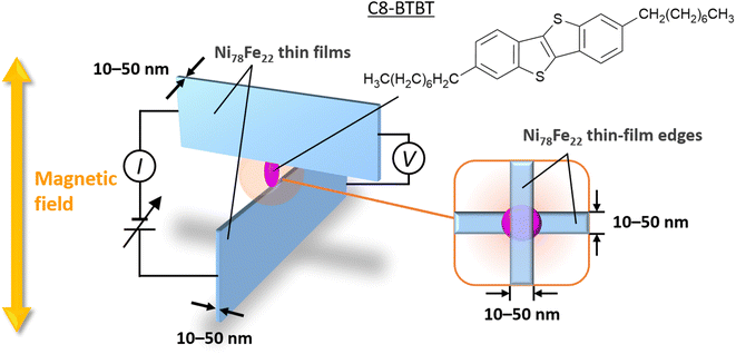 |
| | Fig. 1 Schematic of Ni78Fe22/C8-BTBT/Ni78Fe22 nanojunctions utilizing thin-film edges. The nanojunction consists of C8-BTBT molecules sandwiched between two Ni78Fe22 thin films with crossed edges. The junction area is determined by the film thickness, that is, 10–50 nm thick films could produce 10 × 10 to 50 × 50 nm2 nanojunctions. | |
2. Experimental section
2.1 Fabrication
The procedure followed for the fabrication of the nanojunctions is illustrated in Fig. 2. First, LSP glass substrates of size 10 × 10 × 2 mm3 were prepared and chamfered on both sides (Fig. 2(a)). The glass composition was SiO2–B2O3–Al2O3–Na2O–CaO, and the glass deformation temperature was 503 °C. Ni78Fe22 thin films with thicknesses of 10–50 nm were then deposited onto the glass substrates by sputtering (Fig. 2(b)). A base pressure in the range of 3.0–9.0 × 10⁻⁵ Pa was maintained prior to sputtering. The growth rate of the Ni78Fe22 thin films was 3 nm min−1 at a sputtering power of 60 W (1.0 kV and 60 mA) under Ar pressure of 3.0–5.0 × 10⁻² Pa. Au thin films with a thickness of 14 nm were sputtered onto the chamfered edges of the deposited Ni78Fe22 thin films (Fig. 2(c)). Subsequently, glass substrates of the same composition were stacked on the fabricated Ni78Fe22 thin films by thermal pressing in a N2 atmosphere at a temperature of 513 °C and pressure of 0.25–1.0 MPa (Fig. 2(d)). The obtained samples were cut in half using a high-speed cutting machine (Mecatome T202, Meiwafosis Co., Ltd.; Fig. 2(e)), and their cross-sectional surfaces were first subjected to a two-step mechanical polishing (MP) treatment using Al2O3-based emeries and diamond paste, then a two-step chemical mechanical polishing (CMP) procedure using Al2O3 and SiO2 slurries (Fig. 2(f); the detailed polishing conditions are described in ESI†). Next, C8-BTBT powder was dissolved in 1,2-dichlorobenzene (DCB) to form a 10 mg mL−1 solution, and C8-BTBT thin films were deposited on the polished glass/Ni78Fe22/glass substrate by the off-center spin-coating (OCSC) method23 (Fig. 2(g); the OCSC method is illustrated in detail in Fig. S1†). Finally, another polished glass/Ni78Fe22/glass sample was carefully stacked on the C8-BTBT films by pressing under a pressure of 0.05 MPa. The fabricated nanojunction is illustrated in Fig. 2(h). The reproducibility of the fabrication method is described in ESI.†
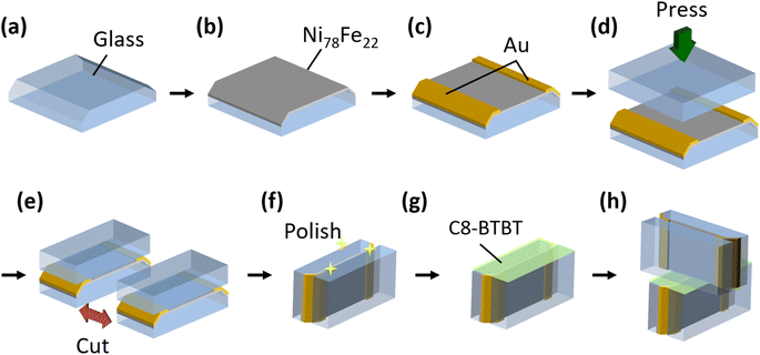 |
| | Fig. 2 Illustration of the fabrication procedure of a Ni78Fe22/C8-BTBT/Ni78Fe22 nanojunction: (a) formation of the LSP glass substrate with chamfered edges. (b) Sputtering of Ni78Fe22 thin films. (c) Sputtering of Au films onto the chamfered edges of the Ni78Fe22 thin films. (d) Thermal pressing of the glass substrate. (e) Cutting the sample. (f) Polishing the cross section of the glass/Ni78Fe22/glass structure. (g) Fabricating C8-BTBT films on the polished glass/Ni78Fe22/glass substrate. (h) Sandwiching C8-BTBT films between the two Ni78Fe22 thin-film edges. | |
2.2 Measurement
The interfacial features of the polished glass/Ni78Fe22/glass samples were examined using transmission electron microscopy (TEM; TECNAI Osiris, FEI) and energy-dispersive X-ray spectroscopy (EDS). Cross-sectional TEM specimens were prepared using the focused ion beam (FIB) technique. The thickness of the Ni78Fe22 thin films was measured using TEM. The surface morphologies and roughness of the polished glass/Ni78Fe22/glass substrates with and without C8-BTBT were analyzed using atomic force microscopy (AFM; Nanocute, SII Nano Technology Inc.). The chemical compositions and structures of C8-BTBT molecules were identified using Fourier transform infrared (FT-IR; FT/IR-4X, JASCO Corporation) spectroscopy. The electrical properties of the Ni78Fe22 thin-film edges, with and without C8-BTBT, were evaluated using a conductive AFM (c-AFM) system equipped with a Rh-coated cantilever (Si-DF3-R). Magnetization curves of the Ni78Fe22 thin films were measured using magneto-optic Kerr effect spectroscopy (MOKE; BH-PI920-HU, NEOARK). The MR curves of the fabricated nanojunctions were evaluated using a four-probe method under a magnetic field of up to ±190 Oe at room temperature.
3. Results and discussion
3.1 Structural and electrical characterization of Ni78Fe22 thin films
Fig. 3(a) shows the cross-sectional TEM image obtained for the 42 nm thick Ni78Fe22 film sandwiched between the two LSP glasses. Films with smooth and clear interfaces can be observed to have successfully formed. Precise formation of a 42 nm thick Ni78Fe22 thin film is important because this thickness directly determines the junction area; that is, 42 nm thick films can produce nanojunctions with an area of 42 × 42 nm2. Fig. 3(b) shows high-angle annular dark field (HAADF)-EDS mapping images of the same sample. The films exhibit smooth and clear interfaces without any diffusion of Ni or Fe atoms into the bulk glass. In some earlier studies, metal atoms were found to diffuse into the LSP materials after deposition.33–37 By contrast, in this study, metal diffusion into the bulk of the LSP materials did not occur at the Ni78Fe22/glass interface. The results indicate that glass/Ni78Fe22/glass can be successfully fabricated by thermal pressing. Fig. 3(c) shows an AFM image of the polished cross-sectional surfaces of the glass/Ni78Fe22 (42 nm)/glass substrate. The roughness of the polished surface measured over the same scanning area of 10 × 20 μm2, shown in Fig. 3(c), does not exceed 0.77 nm. The observed Ni78Fe22 thin-film edge exhibits a convex shape with a height of approximately 5.5 nm, which ensures good contact between the Ni78Fe22 edges and the sandwiched material (C8-BTBT in this study) in the nanojunctions. The heights of the projected edges can be controlled during the second step of the CMP process using SiO2 slurries. Fig. 3(d) shows a c-AFM image of the same specimen, indicating uniform electrical conduction along the Ni78Fe22 edges. Fig. 3(e) shows the I–V characteristics obtained at an arbitrary position on the Ni78Fe22 edges under optimized polishing conditions. The I–V curve is ohmic, suggesting that the Ni78Fe22 edge is not oxidized. In our previous study, contrast enhancement of the Co edge was observed in the scanning electron microscope (SEM) images of glass/Co (14 nm)/glass specimens, which was attributed to the high conductivity of Co.19 However, we did not observe uniform electrical conduction and ohmic behavior during c-AFM studies of Co samples, suggesting the formation of a thin Co oxide layer on the Co edge surface. Therefore, the obtained results in this study indicate that Ni78Fe22 can offer better long-term stability and oxidation resistance than Co. The AFM and c-AFM results reveal that the Ni78Fe22 thin films sandwiched between the LSP glasses can be used as electrodes in the proposed nanojunctions.
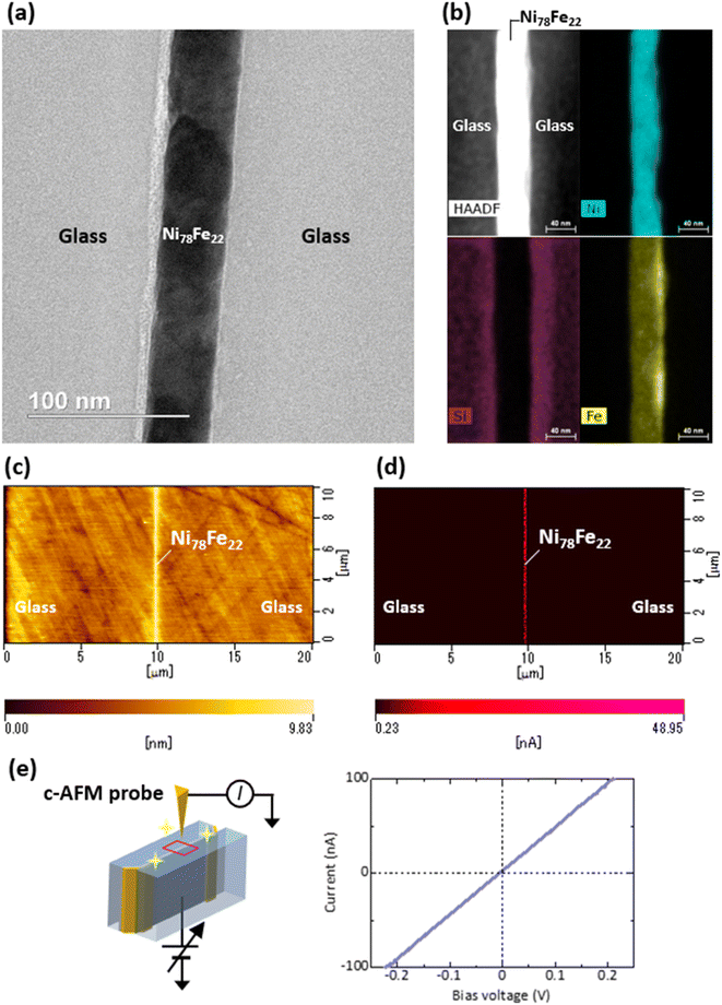 |
| | Fig. 3 (a) Cross-sectional TEM image and (b) HAADF-EDS mapping images obtained for the 42 nm thick Ni78Fe22 film sandwiched between the two LSP glasses. (c) AFM and (d) c-AFM images of the polished surface of the glass/Ni78Fe22 (42 nm)/glass substrates. (e) I–V characteristic of the Ni78Fe22 edge obtained under optimized polishing conditions. Ohmic behavior suggests that the Ni78Fe22 edge is not oxidized. | |
3.2 Structural and electrical characterization of C8-BTBT thin films
After the formation of the C8-BTBT films on the polished surface of the glass/Ni78Fe22 (42 nm)/glass substrates, the roughness of the surface of the C8-BTBT film is measured to be approximately 0.82 nm over a scanning area of 10 × 20 μm2 using AFM. Uniform electrical conduction along the Ni78Fe22 edges is observed in the c-AFM images. The details of AFM and c-AFM studies are described in Fig. S2.† In addition, the measured FT-IR spectra are in good agreement with the reference experimental data for C8-BTBT,38–41 indicating the formation of high-quality C8-BTBT thin films. The detailed measurement conditions and results of the FT-IR study are presented in the ESI.†Fig. 4(a) shows the cross-sectional TEM image obtained for the 2 nm thick C8-BTBT film on the polished surface of the glass/Ni78Fe22 (42 nm)/glass substrates. A film with smooth and clear interfaces is successfully fabricated on the Ni78Fe22 edges. Here, we note that there is a slight curvature in the interface between C8-BTBT films and glass/Ni78Fe22 (42 nm)/glass substrates. This curvature is caused by the structural change of LSP glasses due to the heat generated during TEM observation. The shape of the LSP glasses, which are used for sandwiching Ni78Fe22 thin films, changes with time during TEM observation. Fig. 4(b) shows the local I–V characteristics obtained by c-AFM for the C8-BTBT films on the polished Ni78Fe22 edges. The I–V curve exhibits a clear nonlinear behavior, which can be explained in terms of the space charge limited current (SCLC).42,43 According to Child’s law, the transport carriers injected from a metal layer into the trap-free organic layer can exhibit two different regimes: ohmic conductivity (I ∝ V) at low voltages and square-law behavior (I ∝ V2) at higher voltages, which corresponds to SCLC.42,43 As shown in Fig. 4(b), the obtained experimental results are in good agreement with the theoretical calculation based on Child’s law. The obtained results indicate the successful formation of C8-BTBT films on the Ni78Fe22 edge.
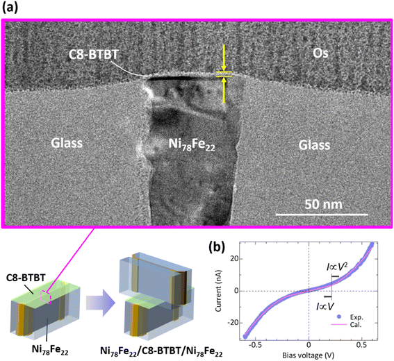 |
| | Fig. 4 (a) Cross-sectional TEM image obtained for 2 nm thick C8-BTBT films on the polished surface of the glass/Ni78Fe22 (42 nm)/glass substrates. (b) I–V characteristics of the polished Ni78Fe22 edge after the formation of C8-BTBT films. The nonlinear behavior can be explained in terms of the SCLC. | |
3.3 Magnetic properties of Ni78Fe22 thin films
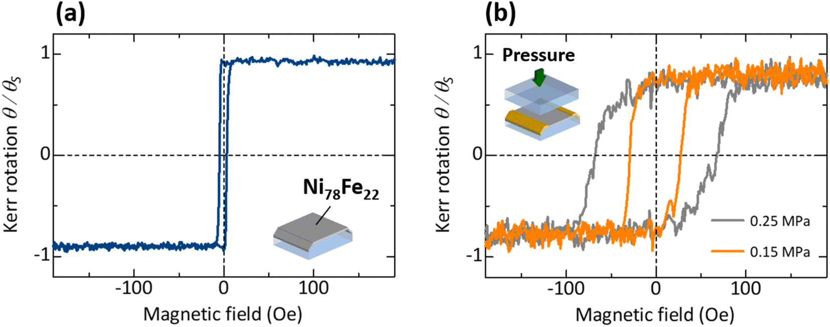
Fig. 5(a) shows the magnetization curve of the 42 nm thick Ni78Fe22 films formed on the LSP glasses. The coercivity is as low as 3 Oe, which is consistent with the typical value for Ni78Fe22 films.44 This result indicates that high-quality Ni78Fe22 thin films can be formed on LSP glasses with regard to magnetic properties. Fig. 5(b) shows the magnetization curve of the Ni78Fe22 films sandwiched between two LSP glasses. The coercivities of Ni78Fe22 thin films increase to 29 and 68 Oe by increasing the applied pressures to 0.15 and 0.25 MPa, respectively, during the thermal pressing process. According to the random anisotropy model, the enhancement in the coercivity is attributed to the increase in the crystal grain size.22 The different coercivities can produce the P and AP configurations, leading to the observation of MR effect. These results indicate that Ni78Fe22 thin films sandwiched between LSP glasses can be used as electrodes for the proposed nanojunctions.
 |
| | Fig. 5 Magnetization curves of the Ni78Fe22 (42 nm) film (a) before and (b) after thermal pressing. The coercivity increases to 29 and 68 Oe by increasing the applied pressure to 0.15 and 0.25 MPa, respectively, during the thermal pressing process. | |
3.4 Electrical properties and MR effect of nanojunctions
Using the described techniques, we fabricate (i) Ni78Fe22/Ni78Fe22 nanojunctions in which two edges of Ni78Fe22 thin films are in direct contact and (ii) Ni78Fe22/C8-BTBT/Ni78Fe22 nanojunctions in which 2 or 4 nm thick C8-BTBT molecules are sandwiched between two edges of Ni78Fe22 thin films. The 42 nm thick Ni78Fe22 films with a coercivity of 29 (68) Oe are used as the top (bottom) electrode. The I–V curves of the fabricated nanojunctions are described in ESI.† The resistance of Ni78Fe22/Ni78Fe22 is low at 82.8 Ω (Fig. S4(a)†), which corresponds to the resistance of electrode short circuit. The resistance of Ni78Fe22/C8-BTBT (2 nm)/Ni78Fe22 nanojunctions is 135.2 Ω (Fig. S4(b)†), which is larger than the resistance of Ni78Fe22/Ni78Fe22. Here, the measured resistance (135.2 Ω) is much smaller than the value estimated using Ohm’s law. In our proposed method, we can fabricate the molecular layer without any interdiffusion of Ni or Fe atoms because the top layer is not deposited on molecules by thermal evaporation or sputtering method. Therefore, Ni or Fe atoms cannot penetrate easily into molecules. This means that the low resistance is not due to the formation of conductive path through Ni or Fe atoms. In addition, during the measurement of I–V characteristics, the bias voltage is only ∼5 mV as shown in Fig. S4 and S5.† Since the metal filaments are generally caused by a high voltage from 0.5 to a few volts,45 the low resistance is not attributed to the formation of short-circuit path originating from the metal filaments. Although the reason for the low resistance is not yet clear, one possibility is the effect of quantized conductance.46–57 Another possibility is that the resistance can change depending on the experimental method, such as nanoindentation, nanoimprinting, lithography, or our newly proposed method using thin-film edges, and materials, i.e., Alq3 or C8-BTBT, in nanoscale devices. The resistance is also sensitive to the shape, such as wires, rings, rectangles, ellipses and circles. In fact, the resistance in nanoscale magnetic tunnel junctions (MTJs) can change depending on experimental methods, materials and shape.58–63 For example, the resistance in Co40Fe40B20/MgO (0.9–1.4 nm)/Co40Fe40B20 nanopillar MTJs with a diameter of 370 nm fabricated using nanosphere lithography is as large as 20–143 kΩ,60 meanwhile the resistance in FeB/MgO (1.0 nm)/FeB nanopillar MTJs with a 200 × 70 nm2 ellipsoidal area fabricated using electron-beam (EB) lithography is small at ∼200 Ω.61 Other examples include the resistance in Co60Fe20B20/Al-oxide (0.6–1.0 nm)/Co60Fe20B20 nano-ring MTJs with an outer diameter of 100 nm and ring-width of 25 nm (corresponding to an effective junction area of 76 × 76 nm2) fabricated using EB lithography is as small as 285–337 Ω,58 and also the resistance in CoFeB/MgO (0.93 nm)/FeB nano-MTJs with a diameter of 21.7 nm fabricated using EB lithography is 12 kΩ.62 Thus, the resistance ranges from ∼100 Ω to ∼MΩ in nanoscale devices. Therefore, it could be possible to show such a small resistance in our proposed nanoscale devices.
Next, we investigate the MR effect of the fabricated Ni78Fe22/Ni78Fe22 and Ni78Fe22/C8-BTBT (2 or 4 nm)/Ni78Fe22 nanojunctions. Fig. 6 shows the MR curves of the Ni78Fe22/Ni78Fe22 and Ni78Fe22/C8-BTBT (2 nm)/Ni78Fe22 nanojunctions. Both the MR curves show similar tendency. In Ni78Fe22/Ni78Fe22 nanojunctions, anisotropic magnetoresistance (AMR) effect is observed. Because the coercivities of the top and bottom Ni78Fe22 electrodes are different, the AMR curves should consist of four peaks, which can be estimated from the magnetization curve. However, only two peaks are observed. This implies that the observed MR effect cannot be understood using a simple AMR model. It can alternatively be explained as follows: the top and bottom Ni78Fe22 electrodes are magnetically coupled at the junction interface. The magnetically coupled Ni78Fe22 contact produces a different coercivity of ∼50 Oe, as estimated from Fig. 5(b). This is consistent with the MR curve shown in Fig. 6(a). Moreover, as shown in Fig. 6(b), no positive MR effect is observed in the Ni78Fe22/C8-BTBT (2 nm)/Ni78Fe22 nanojunctions. The resistance (∼135 Ω) is larger than the measured resistance (∼82 Ω) of the Ni78Fe22/Ni78Fe22 nanojunctions. This means that the electrical conductivities through the 2 nm thick C8-BTBT molecules can be successfully observed in Fig. 6(b). However, the behavior of the MR curve of the Ni78Fe22/C8-BTBT (2 nm)/Ni78Fe22 junctions is similar to that of the Ni78Fe22/Ni78Fe22 junctions. This indicates that the observed MR is due to the AMR in the interfacial Ni78Fe22 close to the C8-BTBT molecules. Here, the AP configuration of magnetization is not realized in the interfacial Ni78Fe22 because of the magnetic coupling between the two edges of the Ni78Fe22 thin films. This suggests that with thicker C8-BTBT layers suppressing the magnetic coupling, the P and AP configurations could be realized in the interfacial Ni78Fe22, leading to a positive MR effect.
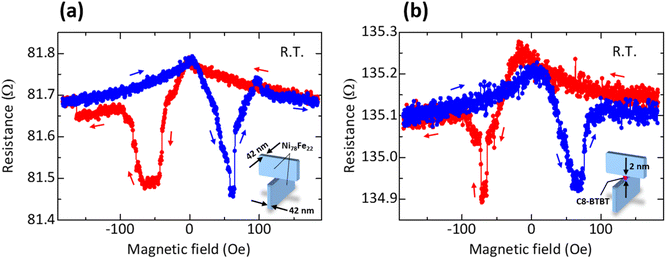 |
| | Fig. 6 MR effect in (a) Ni78Fe22/Ni78Fe22 and (b) Ni78Fe22/C8-BTBT (2 nm)/Ni78Fe22 nanojunctions with a junction area of 42 × 42 nm2 at room temperature. The blue (red) plots represent the results obtained under the forward (reverse) sweeping field. | |
Fig. 7 shows the MR curves of the Ni78Fe22/C8-BTBT (4 nm)/Ni78Fe22 nanojunction at room temperature. A positive MR effect, that is, RAP > RP, is clearly observed. The positive MR cannot be explained by AMR effect. The observation of the positive MR is also one of the evidence to rule out the possibility of electrode short circuit. These reasons are described in ESI.† Thus, the observation of the positive MR effect indicates that a spin signal through C8-BTBT molecules can be successfully observed. This also indicates that the top and bottom Ni78Fe22 electrodes are not magnetically coupled at the junction interface. The magnetic coupling between the two Ni78Fe22 edges can be suppressed by the larger molecular spacing (∼4 nm). Here, we note that the observed MR curves are slightly different from what is expected based on the magnetization curves shown in Fig. 5(b). Such incongruence between the MR curves and magnetization states has also been reported in other studies.1,7,9,14 For example, in Alq3-based MR devices, the top electrode (Co) and bottom electrode (LSMO) showed coercivities of 150 and 30 Oe, respectively, which are not in good agreement with the values 170 and 70 Oe, respectively, estimated from the observed MR effect.1 In another study, the MR effect was observed in Ni/benzene-1,4-dithiol (BDT)/Ni single molecular junctions using mechanically controllable break junction (BJ) method.55 However, it is difficult to compare the MR effect and corresponding magnetization states of electrodes in the BJ method. By contrast, we can precisely investigate both the MR effect and magnetization curves simultaneously by using our proposed method. The results of the investigation show that, because the magnetization states of the Ni78Fe22 thin-film edges adjacent to C8-BTBT molecules are different from those of the Ni78Fe22 thin films obtained by MOKE measurements (Fig. 5(b)), the MR curves show slightly different behaviors, as expected. In addition, the AMR effect can be observed during magnetic-field switching between the P and AP configurations. This also provides strong evidence for attributing the observed positive MR effect to the spin signal through the C8-BTBT molecules. A positive MR effect is also observed at different applied voltages, as shown in Fig. S7.† However, it is difficult to distinguish whether the observed spin signal originates from the tunneling or hopping mechanism. To clarify the mechanism, it is necessary to investigate the temperature dependence of resistance, which will be a future work.
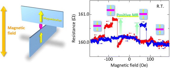 |
| | Fig. 7 MR effect in Ni78Fe22/C8-BTBT (4 nm)/Ni78Fe22 nanojunctions with a junction area of 42 × 42 nm2 at room temperature. The P and AP configurations of magnetization in the two electrodes are also shown. A positive MR effect, that is, RAP > RP, is clearly observed. | |
4. Conclusive remarks
We have successfully fabricated Ni78Fe22/C8-BTBT/Ni78Fe22 nanojunctions using the proposed technique. Consequently, a positive MR effect is observed for the Ni78Fe22/C8-BTBT/Ni78Fe22 nanojunctions at room temperature. This effect indicates that a spin signal through the C8-BTBT molecules can be successfully observed. The results presented in this study can open up new avenues of nanofabrication and the creation of a new research field, “high-mobility molecular nano-spintronics.”
Conflicts of interest
There are no conflicts to declare.
Acknowledgements
This research was supported by the Grants-in-Aid for Scientific Research (B) (No. 21H01397) and Challenging Exploratory Research Program (No. 19K22093) funded by the Japan Society for the Promotion of Science (JSPS), the Dynamic Alliance for Open Innovation Bridging Human, Environment and Materials and the Cooperative Research Program of “Network Joint Research Center for Materials and Devices” funded by the Ministry of Education, Culture, Sports, Science, and Technology (MEXT), and Research Project funded by the Center for Spintronics Research Network (CSRN) at Keio and Tohoku University. The authors would like to express their sincere appreciation to S. Kojima of the Central Service Facilities for Research of Keio University for her expert technical assistance in FIB processing and TEM observations.
References
- Z. H. Xiong, D. Wu, Z. V. Vardeny and J. Shi, Nature, 2004, 427, 821–824 CrossRef CAS PubMed.
- D. Sun, L. Yin, C. Sun, H. Guo, Z. Gai, X.-G. Zhang, T. Z. Ward, Z. Cheng and J. Shen, Phys. Rev. Lett., 2010, 104, 236602 CrossRef PubMed.
- T. D. Nguyen, F. Wang, X.-G. Li, E. Ehrenfreund and Z. V. Vardeny, Phys. Rev. B: Condens. Matter Mater. Phys., 2013, 87, 075205 CrossRef.
- X. Sun, M. Gobbi, A. Bedoya-Pinto, O. Txoperena, F. Golmar, R. Llopis, A. Chuvilin, F. Casanova and L. E. Hueso, Nat. Commun., 2013, 4, 2794 CrossRef.
- D. Sun, E. Ehrenfreund and Z. V. Vardeny, Chem. Commun., 2014, 50, 1781–1793 RSC.
- F. Li, T. Li, F. Chen and F. Zhang, Sci. Rep., 2015, 5, 9355 CrossRef PubMed.
- S. Ding, Y. Tian, Y. Li, W. Mi, H. Dong, X. Zhang, W. Hu and D. Zhu, ACS Appl. Mater. Interfaces, 2017, 9, 15644–15651 CrossRef CAS PubMed.
- L. Guo, Y. Qin, X. Gu, X. Zhu, Q. Zhou and X. Sun, Front. Chem., 2019, 7, 428 CrossRef CAS PubMed.
- Y. Zheng, Y. Feng, D. Gao, N. Zheng, D. Li, L. Jiang, X. Wang, K. Jin and G. Yu, Adv. Electron. Mater., 2019, 5, 1900318 CrossRef CAS.
- D. Li and G. Yu, Adv. Funct. Mater., 2021, 31, 2100550 CrossRef CAS.
- P. Wang, B. B. Chen and X. Wang, Synth. Met., 2021, 273, 116676 CrossRef CAS.
- I. Angervo, M. Saloaro, H. Palonen, H. Huhtinen, P. Paturi, T. Mäkelä and S. Majumdar, Appl. Surf. Sci., 2022, 589, 152854 CrossRef CAS.
- X. Yang, A. Guo, L. Guo, Y. Liu, X. Sun and Y. Guo, ACS Mater. Lett., 2022, 4, 805–814 CrossRef CAS.
- D. Li, Y. Zheng, M. Yang, C. Wei, X. Liu, N. Zheng, W. Zhang, K. Jin and G. Yu, ACS Mater. Lett., 2022, 4, 1065–1073 CrossRef CAS.
- C. Barraud, P. Seneor, R. Mattana, S. Fusil, K. Bouzehouane, C. Deranlot, P. Graziosi, L. Hueso, I. Bergenti, V. Dediu, F. Petroff and A. Fert, Nat. Phys., 2010, 6, 615–620 Search PubMed.
- A. R. Rocha, V. M. García-Suárez, S. W. Bailey, C. J. Lambert, J. Ferrer and S. Sanvito, Nat. Mater., 2005, 4, 335–339 CrossRef CAS PubMed.
- S. Pramanik, C.-G. Stefanita, S. Patibandla, S. Bandyopadhyay, K. Garre, N. Harth and M. Cahay, Nat. Nanotechnol., 2007, 2, 216–219 CrossRef CAS PubMed.
- H. Kaiju, K. Kondo, A. Ono, N. Kawaguchi, J. Won, A. Hirata, M. Ishimaru, Y. Hirotsu and A. Ishibashi, Nanotechnology, 2010, 21, 015301 CrossRef PubMed.
- H. Kaiju, H. Kasa, T. Komine, S. Mori, T. Misawa, T. Abe and J. Nishii, J. Appl. Phys., 2015, 117, 17C738 CrossRef.
- W. Brückner, S. Baunack, M. Hecker, J. Thomas, S. Groudeva-Zotova and C. M. Schneider, Mater. Sci. Eng., B, 2001, 86, 272–275 CrossRef.
- P. Tyagi, E. Friebe and C. Baker, Nano, 2015, 10, 1530002 CrossRef CAS.
- T. Misawa, S. Mori, T. Komine, M. Fujioka, J. Nishii and H. Kaiju, Appl. Surf. Sci., 2016, 390, 666–674 CrossRef CAS.
- Y. Yuan, G. Giri, A. L. Ayzner, A. P. Zoombelt, S. C. B. Mannsfeld, J. Chen, D. Nordlund, M. F. Toney, J. Huang and Z. Bao, Nat. Commun., 2014, 5, 3005 CrossRef PubMed.
- H. Ren, Q. Tang, Y. Tong and Y. Liu, Materials, 2017, 10, 918 CrossRef PubMed.
- D. He, J. Qiao, L. Zhang, J. Wang, T. Lan, J. Qian, Y. Li, Y. Shi, Y. Chai, W. Lan, L. K. Ono, Y. Qi, J.-B. Xu, W. Ji and X. Wang, Sci. Adv., 2017, 3, e1701186 CrossRef PubMed.
- T. Shen, H. Zhou, J. Xin, Q. Fan, Z. Yang, J. Wang, T. Mei, X. Wang, N. Wang and J. Li, Appl. Surf. Sci., 2019, 498, 143822 CrossRef CAS.
- T. Yasuda, L. Han and T. Tsutsui, J. Photopolym. Sci. Technol., 2009, 22, 713–717 CrossRef CAS.
- B. J. Chen, W. Y. Lai, Z. Q. Gao, C. S. Lee, S. T. Lee and W. A. Gambling, Appl. Phys. Lett., 1999, 75, 4010–4012 CrossRef CAS.
- V. A. Dediu, L. E. Hueso, I. Bergenti and C. Taliani, Nat. Mater., 2009, 8, 707–716 CrossRef CAS PubMed.
- X.-D. Liu, S.-L. Zhao, Z. Xu, F.-J. Zhang, T.-H. Zhang, W. Gong, G. Yan, C. Kong, Y.-S. Wang and X.-R. Xu, Chin. Phys. B, 2011, 20, 068801 CrossRef.
- H. Yan, Z. Chen, Y. Zheng, C. Newman, J. R. Quinn, F. Dötz, M. Kastler and A. Facchetti, Nature, 2009, 457, 679–686 CrossRef CAS PubMed.
- Z. Chen, D. Gao, J. Huang, Z. Mao, W. Zhang and G. Yu, ACS Appl. Mater. Interfaces, 2016, 8, 34725–34734 CrossRef CAS PubMed.
- J. H. Cho, D. H. Kim, Y. Jang, W. H. Lee, K. Ihm, J.-H. Han, S. Chung and K. Cho, Appl. Phys. Lett., 2006, 89, 132101 CrossRef.
- C.-Y. Nam, D. Su and C. T. Black, Adv. Funct. Mater., 2009, 19, 3552–3559 CrossRef CAS.
- M. Wang, F. Xie, W. Xie, S. Zheng, N. Ke, J. Chen, N. Zhao and J. B. Xu, Appl. Phys. Lett., 2011, 98, 183304 CrossRef.
- A. Turak, RSC Adv., 2013, 3, 6188–6225 RSC.
- Y. Xu, C. Liu, H. Sun, F. Balestra, G. Ghibaudo, W. Scheideler and Y.-Y. Noh, Org. Electron., 2014, 15, 1738–1744 CrossRef CAS.
- Y. Li, C. Liu, M. V. Lee, Y. Xu, X. Wang, Y. Shi and K. Tsukagoshi, J. Mater. Chem. C, 2013, 1, 1352–1358 RSC.
- Y. Shibata, T. Matsuzaki, T. Ishinabe and H. Fujikake, J. Cryst. Growth, 2018, 492, 98–104 CrossRef.
- J. Mai, N. Tang, W. He, Z. Zou, C. Luo, A. Zhang, Z. Fan, S. Wu, M. Zeng, J. Gao, G. Zhou, X. Lu and J.-M. Liu, Nanoscale Res. Lett., 2019, 14, 169 CrossRef PubMed.
- Z. Wang, H. Guo, J. Li, L. Wang and G. Dong, Adv. Mater. Interfaces, 2019, 6, 1801736 CrossRef.
- R. W. Smith and A. Rose, Phys. Rev., 1955, 97, 1531–1537 CrossRef.
- M. A. Lampert, Phys. Rev., 1956, 103, 1648–1656 CrossRef.
- P. Saravanan, J.-H. Hsu, C.-L. Tsai, A. K. Singh and P. Alagarsamy, IEEE Trans. Magn., 2015, 51, 2006604 Search PubMed.
- F. Zahoor, T. Z. A. Zulkifli and F. A. Khanday, Nanoscale Res. Lett., 2020, 15, 90 CrossRef PubMed.
- H. Park, J. Park, A. K. L. Lim, E. H. Anderson, A. P. Alivisatos and P. L. McEuen, Nature, 2000, 407, 57–60 CrossRef PubMed.
- J. Park, A. N. Pasupathy, J. I. Goldsmith, C. Chang, Y. Yaish, J. R. Petta, M. Rinkoski, J. P. Sethna, H. D. Abruña, P. L. McEuen and D. C. Ralph, Nature, 2002, 417, 722–725 CrossRef PubMed.
- W. Liang, M. P. Shores, M. Bockrath, J. R. Long and H. Park, Nature, 2002, 417, 725–729 CrossRef PubMed.
- F. Chen, X. Li, J. Hihath, Z. Huang and N. Tao, J. Am. Chem. Soc., 2006, 128, 15874–15881 CrossRef PubMed.
- M. Kiguchi, O. Tal, S. Wohlthat, F. Pauly, M. Krieger, D. Djukic, J. C. Cuevas and J. M. van Ruitenbeek, Phys. Rev. Lett., 2008, 101, 046801 CrossRef PubMed.
- M. Kiguchi, Appl. Phys. Lett., 2009, 95, 073301 CrossRef.
- K. Yokota, M. Taniguchi, M. Tsutsui and T. Kawai, J. Am. Chem. Soc., 2010, 132, 17364–17365 CrossRef PubMed.
- S. Schmaus, A. Bagrets, Y. Nahas, T. K. Yamada, A. Bork, M. Bowen, E. Beaurepaire, F. Evers and W. Wulfhekel, Nat. Nanotechnol., 2011, 6, 185–189 CrossRef PubMed.
- S. T. Schneebeli, M. Kamenetska, Z. Cheng, R. Skouta, R. A. Friesner, L. Venkataraman and R. Breslow, J. Am. Chem. Soc., 2011, 133, 2136–2139 CrossRef PubMed.
- R. Yamada, M. Noguchi and H. Tada, Appl. Phys. Lett., 2011, 98, 053110 CrossRef.
- S. K. Lee, R. Yamada, S. Tanaka, G. S. Chang, Y. Asai and H. Tada, ACS Nano, 2012, 6, 5078–5082 CrossRef CAS PubMed.
- T. Nakazumi, S. Kaneko, R. Matsushita and M. Kiguchi, J. Phys. Chem. C, 2012, 116, 18250–18255 CrossRef CAS.
- X. F. Han, Z. C. Wen, Y. Wang, L. Wang and H. X. Wei, AAPPS Bull., 2008, 18, 24–32 CAS.
- S. Ikeda, K. Miura, H. Yamamoto, K. Mizunuma, H. D. Gan, M. Endo, S. Kanai, J. Hayakawa, F. Matsukura and H. Ohno, Nat. Mater., 2010, 9, 721–724 CrossRef CAS PubMed.
- W. G. Wang, A. Pearse, M. Li, S. Hageman, A. X. Chen, F. Q. Zhu and C. L. Chien, Sci. Rep., 2013, 3, 1948 CrossRef CAS PubMed.
- K. Yakushiji, A. Fukushima, H. Kubota, M. Konoto and S. Yuasa, Appl. Phys. Express, 2013, 6, 113006 CrossRef.
- K. Watanabe, B. Jinnai, S. Fukami, H. Sato and H. Ohno, Nat. Commun., 2018, 9, 663 CrossRef CAS PubMed.
- L. Rehm, G. Wolf, B. Kardasz, M. Pinarbasi and A. D. Kent, Appl. Phys. Lett., 2019, 115, 182404 CrossRef.
|
| This journal is © The Royal Society of Chemistry 2022 |
Click here to see how this site uses Cookies. View our privacy policy here. 
 Open Access Article
 This Open Access Article is licensed under a Creative Commons Attribution-Non Commercial 3.0 Unported Licence
 c,
Tomoyuki
Akutagawa
c,
Tomoyuki
Akutagawa