
 Open Access Article
 This Open Access Article is licensed under a
 Creative Commons Attribution 3.0 Unported Licence
Ultrafast photoresponse of vertically oriented TMD films probed in a vertical electrode configuration on Si chips†
Topias
Järvinen‡
 *a,
Seyed-Hossein
Hosseini Shokouh‡
*a,
Sami
Sainio
ab,
Olli
Pitkänen
a and
Krisztian
Kordas
a
*a,
Seyed-Hossein
Hosseini Shokouh‡
*a,
Sami
Sainio
ab,
Olli
Pitkänen
a and
Krisztian
Kordas
a
aMicroelectronics Research Unit, Faculty of Information Technology and Electrical Engineering, University of Oulu, FI-90014 Oulu, Finland. E-mail: topias.jarvinen@oulu.fi; seyed.hosseinishokouh@oulu.fi
bSLAC National Accelerator Laboratory, Stanford University, Stanford, CA 94025, USA
First published on 5th July 2022
Abstract
Integrated photodetectors based on transition metal dichalcogenides (TMDs) face the challenge of growing their high-quality crystals directly on chips or transferring them to the desired locations of components by applying multi-step processes. Herein, we show that vertically oriented polycrystalline thin films of MoS2 and WS2 grown by sulfurization of Mo and W sputtered on highly doped Si are robust solutions to achieve on-chip photodetectors with a sensitivity of up to 1 mA W−1 and an ultrafast response time in the sub-μs regime by simply probing the device in a vertical arrangement, i.e., parallel to the basal planes of TMDs. These results are two orders of magnitude better than those measured earlier in lateral probing setups having both electrodes on top of vertically aligned polycrystalline TMD films. Accordingly, our study suggests that easy-to-grow vertically oriented polycrystalline thin film structures may be viable components in fast photodetectors as well as in imaging, sensing and telecommunication devices.
Introduction
Among 2-dimensional (2D) materials, transition metal dichalcogenides (TMDs) such as disulfides and diselenides of Mo, W, V and Ti, show great potential for optoelectronic applications due to their thickness dependent intrinsic band gap,1,2 optical absorption in the visible spectrum,3,4 polarization dependency,5–8 high in-plane carrier mobility,9,10 and good chemical and thermal stability.11,12 While relatively weak, interlayer van der Waals forces allow easy exfoliation, single layers are mechanically strong which permits the fabrication of the TMD films into robust photodevices. As large-area growth of high-quality mono or few-layered TMDs, e.g., on the wafer size, is not a mature technology yet,13,14 integrated optoelectronic devices of TMDs are mostly based on (i) small size single or few-layered flakes transferred from the growth substrate to the chip or (ii) large-area multilayers15 and bulk materials grown directly on chips.16,17In most of the cases, lateral metal–semiconductor–metal electrode configurations are applied, which are optimal if the 2D crystal has lateral orientation. However, when the semiconducting layer is a thick polycrystalline film or it is thin but vertically aligned, the lateral electrode setup compromises the device response speed,18 which is an important property in applications such as in fast photodetectors, imaging and telecommunication.19 For this reason, thin films of TMDs with vertically oriented layers in the polycrystalline structure that are probed through vertical contacts have immense potential to compete with conventional devices based on planar single or few-layered structures. In addition, in vertically oriented devices, direct edge-contact of the 2D semiconductor with the metal electrodes provides a lower contact resistance20 than on the 2D planes of planar devices, and this further improves the device response speed, which is several orders of magnitude higher than in the lateral electrode arrangement (Table 1).
| Device | TMD synthesis method | Rise/decay time | Photoresponse (A/W) | Electrode geometry and material | Ref |
|---|---|---|---|---|---|
| MoS2 and WS2 on Si | Sulfurization | 250/400 ns | 1 × 10⁻³ | Vertical, Pt | This work |
| MoS2 and WS2 on Si | Sulfurization | 90–190 μs/150–470 μs (MoS2) | 5.5 × 10⁻⁶ (MoS2) | Lateral, Pt | 21 |
| 40 μs/80–130 μs (WS2) | 5.3 × 10⁻⁶ (WS2) | ||||
| PtSe2 on GaAs | Selenization | 5.5/6.5 μs | 262 × 10−3 | Vertical, Ag (top) | 22 |
| MoS2/Cu2ZnS n–p junction on Si/SiO2 | CVD | 81/79 ms | 141 × 10−3 | Lateral, Au | 23 |
| MoS2 on Si | Sputtering | 3/40 μs | ∼300 × 10−3 | Vertical, Ag | 14 |
| Few-layered HfS2 on Si/SiO2 | CVD | 24/24 ms | — | Lateral | 24 |
| Au-nanoparticle decorated MoS2 nanoflakes on Si/SiO2 | CVD | <100/<100 ms | 24 × 10−3 | Lateral, Au | 25 |
| SnS2 nanoflakes on Si/SiO2 | CVD | 400 μs/560 μs | 354.4 | Lateral, Au/Cr | 26 |
| WS2/ZnO heterostructure on FTO/glass | Sputtering | 0.8/2.2 ms | 2.7 | Vertical, ITO | 27 |
| MoSe2 on Si | Sputtering | 270/350 ns | 93–270 × 10−3 | Vertical, graphene | 19 |
| MoS2 on Si/Ag | CVD | 56/825 ns | 908.2 × 10⁻³ | Vertical, Ag | 28 |
In this paper, the optoelectronic properties of vertically oriented and probed MoS2 and WS2 films grown on Si substrates are assessed, and compared to their counterparts having lateral electrode geometries we reported earlier.21 While the vertical setup is found to show good enhancement of photosensitivity, the response time of the devices improves significantly, by two orders of magnitude, compared to identical TMD films on Si/SiO2 chips but with lateral top contacts. Accordingly, our present study confirms that the synthesis of TMDs by sulfurization of metal thin films, and the subsequent application of sputtered semitransparent metal top electrodes offer a feasible approach to produce large-scale on-chip devices having ultrafast photodetection properties in the visible spectrum.
Experimental
Materials synthesis
Highly doped p++ Si wafers were cut into 10 × 10 mm2 square pieces using a laser (LPKF ProtoLaser U3, CMA Oulu). Mo or W films were then deposited on each wafer by sputtering (Torr International Physical Vapor Deposition (PVD) System, CMA Oulu, 2.4 × 10⁻³ torr Ar atmosphere, 155 W power, 1.2 Å s−1 deposition rate and 165 s total deposition time for Mo; 165 W power, 0.8–0.9 Å s−1 deposition rate and total deposition time of 235 s for W) with a nominal thickness of 20 nm (measured with Sigma instruments SQC-122c thin film deposition controller, CMA Oulu). The sulfurization process of the metal films follows the procedure described earlier. In short, Mo or W coated Si chips were inserted into a 2′′ tube furnace together with 1.00 g of sulfur powder (Sigma-Aldrich 215236) loaded in a ceramic boat. After evacuating with a dry rotary pump to <1 Torr pressure and purging the tube three times with N2 the temperature was raised to and kept at 800 °C for one hour, while keeping a constant 400 sccm flow of N2 during the synthesis.Materials characterization
The structure, orientation and composition of the films were analyzed using X-ray diffraction in the grazing incidence configuration (GIXRD, Co source, Rigaku SmartLab 9 kW) and Raman spectroscopy (Horiba Jobin-Yvon LabRAM HR800 with a laser wavelength of 488 nm). The GIXRD results were converted to equivalent Cu X-ray source patterns to allow for direct comparison to previous results.29 The data were plotted in OriginPro® 2020.Cross-sections of the sulfurized films were prepared using a focused ion beam (FIB, FEI Helios DualBeam) and analyzed by transmission electron microscopy (TEM, JEOL JEM-2200FS EFTEM/STEM). In addition to the TEM/STEM imaging, energy-dispersive X-ray (EDX) spectroscopy and electron diffraction were performed to assess the chemical composition and crystal orientation.
To evaluate the chemistry, oxidation and potential contamination of the films, XPS and XAS spectra were collected at the Stanford Synchrotron Radiation Light source (SSRL) magnet beamline 8−2 that is equipped with a spherical grating monochromator, operated using 40 × 40 μm2 slits, resulting in a resolution of around 200 meV. The spot size at the interaction point was around 1 × 1 mm2, and the total flux was in the order of 1010 photons per s without any visible beam damage even for extended exposure. The X-ray energy for the C 1s, N 1s, and O 1s edges was scanned from 260 to 350, 380 to 430, and 520 to 560 eV, respectively. The XAS data in the TEY were collected using a drain current (amplified by using a Keithley picoammeter), and the AEY and XPS data were collected using a cylindrical mirror analyzer, operated with a pass energy of 200 eV and 50 eV, respectively. The incoming flux was recorded using a Ni grid with an Au sputtered film (called the i0). The data collected using the i0 follows the same procedure as the TEY measurements mentioned above. To normalize the XAS data, the slope of the linear background was varied within a small range to keep both the area and edge jump constant across the dataset. Before the peak fitting, the data was energy corrected and aligned to the C 1s sp2 π* at 285.2 eV. Furthermore, the C 1s, O 1s, and N 1s regions refer to the area normalized over the π and σ regions. More details of data normalization and energy correction can be found in ref.30 The XAS and XPS data analyses are carried out using OriginPro® 2020 software. Additional topology and structural analyses were performed by means of AFM and SEM/EDX on similar TMD films in our earlier study.29
Device fabrication and photoconductivity measurements
The semitransparent top electrode on the chips was made by sputtering a thin Pt film with 8 nm thickness (Agar Auto Sputter Coater, Agar Scientific Ltd) through a laser-cut shadow mask (polycrystalline alumina wafer with 150 μm thickness having a 200 × 200 μm2 square pattern opening). The samples were then mounted onto a gold bottom electrode by applying silver paste.The photoconductivity measurement setup is derived from the one used in our previous studies;21,31 a constant bias of 3 V is applied to the sample by using a sourcemeter (Keithley 2636A SYSTEM SourceMeter®) connected in series with a 1 MΩ load resistor. Three different lasers (Coherent® OBIS™ Laser System, TEM00 mode, with wavelengths of 661 nm, 552 nm, and 401 nm and 1/e2 beam diameters of 9 mm, 7 mm, and 8 mm, respectively) are modulated by using a signal generator (33220A, Agilent Technologies, Inc.) applying square waves with a duty cycle from 5% to 50% and frequency from 10 kHz up to 1 MHz depending on the laser wavelength. The signal generator is also used to trigger the oscilloscope (Agilent InfiniiVision DSO-X 3024A with 10 MΩ probe) connected in parallel with the load resistor. The acquired oscilloscope data are then analyzed using OriginPro® 2020 software to resolve the photocurrent, sensitivity, and response times.
Results
Structure and chemistry of TMD films
The Raman spectra of the TMD films (Fig. 1(a) and (b) for MoS2 and WS2, respectively) indicate that the films are multilayered and crystalline.29,32,33 The two main peaks for MoS2 at 384 and 410 cm−1 resemble the in-plane (E12g) and out-of-plane (A1g) vibrations, respectively.34 Likewise, WS2 (E12g) and (A1g) peaks at 357 and 422 cm−1 agree with those in the literature and imply a multilayered structure.35 The longitudinal acoustic mode vibrations (LA) and harmonics (2LA and 4LA) appear for WS2 at 175, 298 and 707 cm−1, respectively.33 In addition to the peaks attributed to the TMD films, the measurements include a background noise level reference (Fig. 1(a)) as well as a pure silicon reference at 520 cm−1 (Fig. 1(b)).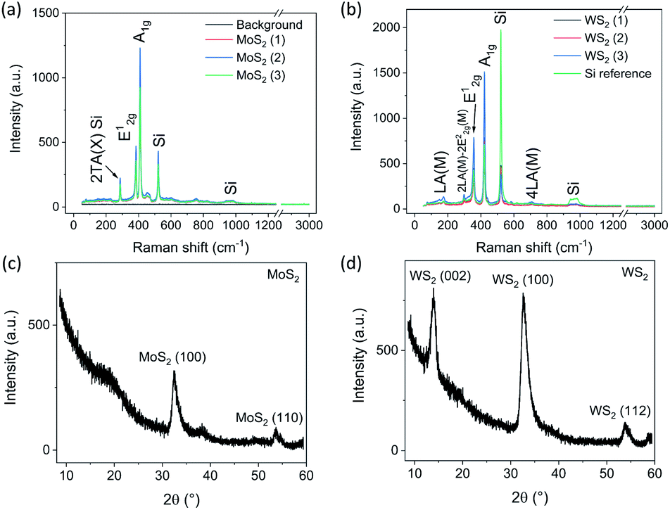 | ||
| Fig. 1 Raman spectra and XRD patterns of the TMD films. Raman spectra of the MoS2 (a) and WS2 (b) films labeled with corresponding phases. The irrelevant parts after 1200 cm−1 have been cut out. GIXRD patterns of MoS2 (c) and WS2 (d). Note that the 2θ angles of the original patterns obtained using a Co source are converted to the corresponding 2θ angles of the Cu source to enable direct comparison with the references. | ||
X-ray diffraction patterns collected in the grazing incidence configuration (Fig. 1(c) and (d) for MoS2 and WS2, respectively) show reflections of MoS2 including (100) at 32.5° (PDF 75-1539) and (110) at 53.7° (PDF 73-1508). The lack of the (002) reflection implies a good vertical orientation of the 2D layers. In contrast, in the pattern of the WS2 film, the reflection of (002) at 13.9° (although having small relative intensity, PDF 08-0237) indicates that the grains of the 2D layer stacks are somewhat distorted.21
TEM analysis of the pure metal films reveals that the actual thicknesses are around 24–26 nm, which are slightly more than the originally specified nominal values of 20 nm. The sulfurized films show slightly varying thicknesses, approximately 55–61 nm for MoS2 and 85–110 nm for WS2. The latter is overall less uniform and has partially detached porous sections. Likewise, while the vertical orientation of MoS2 is clearly visible, WS2 shows somewhat misaligned grains of the crystalline layered structures (Fig. 2(a) and (b) for MoS2 and WS2, respectively). The same feature is visible in the electron diffraction patterns (Fig. 2(c) and (d) for MoS2 and WS2, respectively), in which for MoS2 we observe clear diffraction spots of the (002) plane, whereas for WS2 a diffraction ring is superposed on the spots due to the partial misalignment of the grains. The lattice spacings of the (002) plane measured from high-magnification TEM images are 6.5 ± 0.1 Å and 6.6 ± 0.1 Å for WS2 and MoS2, respectively. The corresponding values obtained from the electron diffraction patterns are somewhat lower (both 6.3 ± 0.1 Å).
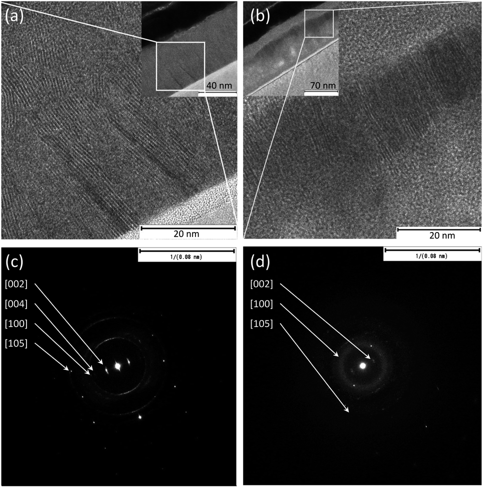 | ||
| Fig. 2 TEM images of cross-sections of (a) MoS2 and (b) WS2 grown on Si. Insets show complete films on Si substrates. Panels (c) and (d) display the corresponding electron diffraction patterns. | ||
EDX analysis of the film cross-sections gives a rough estimate of film stoichiometry (Table S1†). While the metal to sulfur ratio in MoS2 appears to be very close to the 1![[thin space (1/6-em)]](https://www.rsc.org/images/entities/char_2009.gif) :2, WS2 contains a considerable amount of oxygen, which might be due to the chemical instability of WS2 at the crystal edges. Anyhow, despite the large amount of oxygen in the lattice, XRD and Raman analyses do not exhibit any phases of tungsten oxides.29
:2, WS2 contains a considerable amount of oxygen, which might be due to the chemical instability of WS2 at the crystal edges. Anyhow, despite the large amount of oxygen in the lattice, XRD and Raman analyses do not exhibit any phases of tungsten oxides.29
Consequently, to have better insight into the chemistry of the thin films, we carried out further analyses using X-ray photoelectron and absorption edge spectroscopies (XPS and XAS, respectively). The XPS spectra of the MoS2 and WS2 samples show a carbon content which cannot be assigned to metal–carbon bonding indicating the presence of adsorbed carbon (Fig. 3(a) and (b)). In contrast, the O 1s peak reveals the oxygen–metal bonding in addition to adsorbed oxygen. For the MoS2 sample (Fig. 3(c)), the peak at 530.6 eV can be attributed to the Mo–O bond in addition to the adsorbed oxygen and hydroxyl/carboxyl groups at 531.4 and 532.4 eV, respectively.36–38 The resolved O 1s peak of WS2 (Fig. 3(d)) also indicates adsorbed oxygen (531.6 eV), hydroxyl/carboxyl groups (532.4 eV), and W–O bonds (530.7 eV).39,40
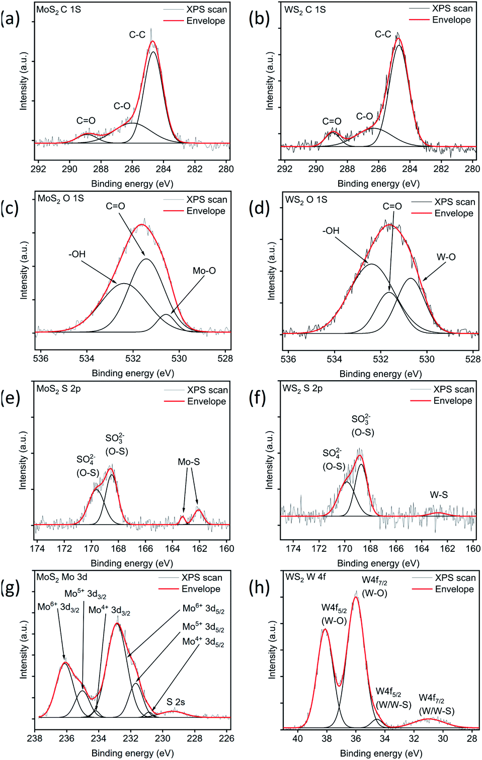 | ||
| Fig. 3 XPS analysis for carbon (a and b), oxygen (c and d), sulfur (e and f), molybdenum (g) and tungsten (h) bands. | ||
The Mo 3d and W 4f spectra also show the oxidation of metals. For instance, the Mo 3d spectrum (Fig. 3(g)) can be fitted with several peaks that correspond to the 4+, 5+ and 6 + oxidation states of molybdenum.37,41–43 Likewise, the W 4f spectrum (Fig. 3(h)) reveals the W–O bonds at 36.0 and 38.1 eV in addition to the W 4f7/2 (31.0 eV) and W 4f5/2 (34.6 eV) doublets of the W–S bond.38,39,44–47
While resolving sulfur-oxygen bonding from O 1s spectra is impossible, the S 2p spectra reveal the sulfur-oxygen bonding. For MoS2, the peaks (Fig. 3(e)) can be resolved as a doublet with components at 162.0 and 163.3 eV of S 2p3/2 and S 2p1/2 of the Mo–S bond,36,48 while the other two peaks at 168.5 and 169.6 eV imply the presence of sulfite/sulfate (SO32−/SO42−) traces.37,49 In the case of WS2, the S 2p spectrum (Fig. 3(f)) also indicates the presence of SO32− (168.7 eV) and SO42− (169.8 eV)38,49 in addition to the W–S bond (162.7 eV). The peak assignments are listed in the ESI (Table S2†).
To further evaluate the contamination and oxidation of the thin films, the C, and O K edge absorption spectra of the WS2 and MoS2 samples were collected at an incidence angle of 55° (magic angle) along with the Mo M2,3 edges at grazing and normal incidence angles of 20°, 55° and 90°. The Auger electron yield (AEY) and total electron yield (TEY) C1s spectra with a missing exciton signature at 291.65 eV, and clear σ* resonance above circa 292 eV indicate the lack of long-range order in the sp2 network (Fig. S1†).30,50 Moreover, the absence of metal-carbon bonding features, same as in the XPS data, implies the presence of carbon as a contaminant (organic compound) on the MoS2 and WS2 thin film surfaces. Especially for the MoS2 sample, Mo M-edge spectra confirm the absence of metal-carbon bonding, for there is no peak ca. 395.4 eV.51
On the other hand, the O K edge absorption spectra, containing oxygen–metal bonding features, reveal the partial surface oxidation of the MoS2 and WS2 samples. In agreement with the EDX data and O K edge absorption spectra, the Mo M-edge spectra show an oxidation state of +652 (instead of +4) for the Mo atom, further supporting the surface oxidation of the MoS2 sample. The comprehensive data analysis and peak assignment are provided in the ESI (Fig. S1–S3 and Tables S3, S4†).
Photoresponse of vertically aligned TMD films measured with vertical probing
Despite the impurities and oxidation especially in the case of WS2, both films show excellent response to illumination with laser pulses in the visible range, Fig. 4. The measured photocurrents are strongly dependent on the applied laser power at each wavelength and can be fitted well using a simple power function (y = axb). The exponents fitted from the calculated mean values (Table 2) show variance between 0.43 and 0.68, which correspond to mid-gap states in the semiconductor, scattering events and possibly even saturable absorption,53,54 and are similar to reported values for 2D TMD materials such as single-layered WS2 (0.4),55 as well as multilayered WS2 (0.24–0.38) and MoS2 (0.35–0.67).21,56 The measurements at 401 nm introduced persistent photoconductivity, which could partly be attributed to traps due to the oxidation of the film. This was addressed by reducing the duty cycle from 50% to 5% which also lowered the photocurrent compared to the 552 and 661 nm measurements performed at 50%. Due to different duty cycles, wavelength dependency of the photoresponses cannot be accurately determined.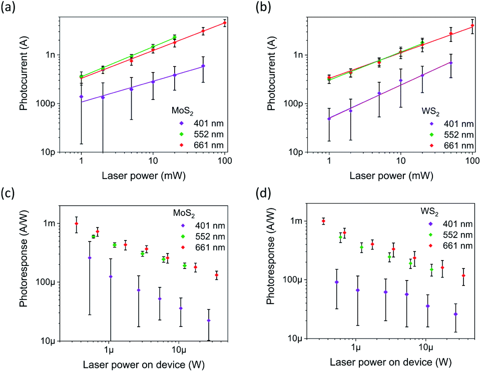 | ||
| Fig. 4 Photocurrents (a and b) and photoresponses (c and d) for MoS2 and WS2 photodevices, respectively. | ||
| Wavelength (nm) | MoS2 | WS2 |
|---|---|---|
| 401 | 0.43 | 0.68 |
| 552 | 0.62 | 0.58 |
| 661 | 0.57 | 0.53 |
In order to make an accurate assessment of the photosensitivity, the incident laser beam power on the illuminated square-shaped electrode is calculated by integrating the Gaussian beam over the electrode area, also considering the incidence angle of 70°. In addition, reflectance and absorbance of the 8 nm thick Pt top electrode are accounted for. Furthermore, as the vertical TMD structures have considerably low conductivity in the lateral direction, we assumed that photo-carriers generated outside the electrode covered film have negligible contribution to the photocurrent. The as-obtained maximum photosensitivity values are 0.99 mA W−1 for MoS2 and 1.00 mA W−1 for WS2, which are over two orders of magnitude higher than those measured with horizontal electrodes in our previous study.21 This difference can partially account for the differences in the electrode areas but even the raw photocurrent values are considerably higher.
The most remarkable difference between the electrode configurations is undisputed, when analyzing the response times. Statistics were collected from the 10 kHz signals at 10 mW for all wavelengths (Fig. 5(c)). Examples for raw waveform signals used for statistics are presented in the ESI (Fig. S4†). As the timescale resolution did not provide accurate exponential fits at the 10 kHz signal, the time constants for the rise and decay transients were calculated from the corresponding 10% and 90% values of the photocurrents providing time constants in the range of a few microseconds. However, when analyzing the waveforms at higher frequencies such as at 1 MHz (Fig. 5(a) and (b) for MoS2 and WS2, respectively), it becomes clear that the actual rise and fall times are well below microseconds for the vertical electrode configuration (approx. 250 ns and 400 ns, respectively). The 50 point averaged signals were also fitted with double exponentials to determine the time constants more precisely (Table S5†). The noise introduced by the measurement setup as well as the 50 kHz upper limit for modulating the 552 nm laser prevent a more comprehensive set of measurements at higher frequencies. The vertical electrode configuration is presented in Fig. 5(d), while response time statistics and the lateral electrode configuration collected and adapted from our previous study are shown in Fig. 5(e) and (f), respectively.21
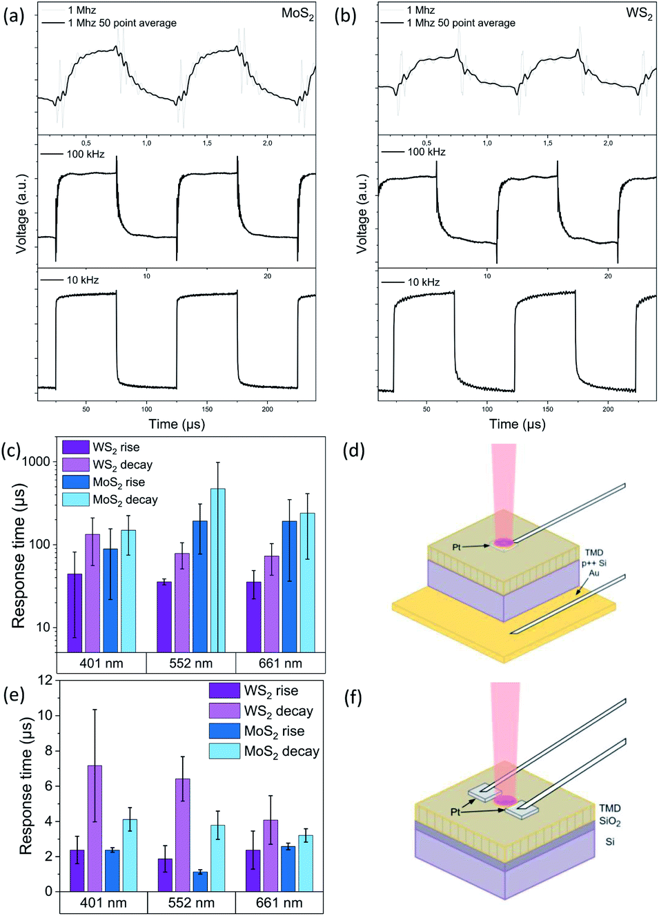 | ||
| Fig. 5 Plotted photoresponses for a vertical electrode configuration at 10 kHz, 100 kHz and 1 MHz for MoS2 (a) and WS2 (b). Response time statistics (c) and measurement setup (d) for the vertical electrode configuration (this study). Respective statistics (e) and setup (f) for lateral electrodes reported in our previous study.17 | ||
The striking difference between the photocurrents and photoresponse speeds measured between the lateral and vertical contacts on vertically aligned 2D TMD crystals stems from a number of events. The crystal anisotropy and the presence of tunneling barriers at the van der Waals interlayers result in direction dependent carrier mobility and electron–phonon interactions which favor in-plane transport.57 The presence of long-life interlayer excitons58 that form between electron and hole adjacent layers induces local polarization and may influence carrier generation and transport. Furthermore, although it is known that point defects59 in the 2D layers can enhance interlayer transport (within the grains), our films are polycrystalline, i.e., the vertically oriented crystals share boundaries complicating the picture even further. As such grain boundaries act as scattering centers, enhance the recombination of photogenerated carriers, and also introduce trap states and barriers, transport60 in the horizontal direction across vertically oriented grains is expected to be significantly limited compared to transport in the vertical direction, in qualitative agreement with our experimental data. It is worth noting that due to the polycrystalline nature of the vertically oriented grains in the films, light polarization dependency unlike in laterally oriented, anisotropic TMD films and flakes5–8 is not expected.
Conclusions
Photocurrent measurements with visible laser pulses on vertically oriented and probed MoS2 and WS2 films indicate a significant improvement in both photosensitivity and response times with reference to those measured with horizontal probe setups. The photosensitivity was found to increase by an order of magnitude, whereas the photocurrent rise and decay times decreased by two orders of magnitude to less than 1 μs because of the enabled in-plane carrier transport and thus, reduced scattering/recombination of photogenerated carriers. The response times could be further enhanced by limiting capacitive effects between the substrate and top electrode as well as minimizing the resistance at contact interfaces between the TMD film and electrodes. Accordingly, our study suggests that in photodetector applications, vertically oriented polycrystalline TMD films shall be probed across the film. Furthermore, as the size of the device is only limited by the dimensions of the semitransparent top electrode, our study suggests the possibility of fabricating sensor arrays with a high spatial resolution for advanced photodetector applications. The direct on-chip synthesis method providing large-scale films brings opportunities for scale-up production and commercial applications, provided that the film homogeneity and packaging are optimized. Furthermore, as micropatterned TMD films can be produced by a variety of lithography based methods,61–63 optimization of on-chip vertical in-plane device performance by adjusting the geometry is enabled and expected in subsequent studies.Author contributions
Conceptualization – T. Järvinen, S.-H. H. Shokouh, K. Kordas. Investigation – T. Järvinen, S.-H. H. Shokouh, O. Pitkänen, S. Sainio. Supervision – K. Kordas. Visualization – T. Järvinen, S.-H. H. Shokouh. Writing (original draft) – T. Järvinen, S.-H. H. Shokouh. Writing (review & editing) – T. Järvinen, S.-H. H. Shokouh, K. Kordas.Conflicts of interest
There are no conflicts to declare.Acknowledgements
Metal film deposition and TEM analysis were carried out with the support of the Centre for Material Analysis, University of Oulu, Finland. Use of the Stanford Synchrotron Radiation Lightsource, SLAC National Accelerator Laboratory, was supported by the U.S. Department of Energy, Office of Science, Office of Basic Energy Sciences under contract no. DE-AC02-76SF00515.Notes and references
- K. F. Mak, C. Lee, J. Hone, J. Shan and T. F. Heinz, Phys. Rev. Lett., 2010, 105, 136805 CrossRef PubMed.
- A. Splendiani, L. Sun, Y. Zhang, T. Li, J. Kim, C.-Y. Chim, G. Galli and F. Wang, Nano Lett., 2010, 10, 1271–1275 CrossRef CAS PubMed.
- M. Bernardi, M. Palummo and J. C. Grossman, Nano Lett., 2013, 13, 3664–3670 CrossRef CAS PubMed.
- Y. Li, A. Chernikov, X. Zhang, A. Rigosi, H. M. Hill, A. M. van der Zande, D. A. Chenet, E.-M. Shih, J. Hone and T. F. Heinz, Phys. Rev. B, 2014, 90, 205422 CrossRef.
- T. Fan, Z. Xie, W. Huang, Z. Li and H. Zhang, Nanotechnology, 2019, 30, 114002 CrossRef CAS PubMed.
- H. Qiao, Z. Huang, X. Ren, S. Liu, Y. Zhang, X. Qi and H. Zhang, Adv. Opt. Mater., 2020, 8, 1900765 CrossRef CAS.
- Z. Guo, R. Cao, H. Wang, X. Zhang, F. Meng, X. Chen, S. Gao, D. K. Sang, T. H. Nguyen, A. T. Duong, J. Zhao, Y.-J. Zeng, S. Cho, B. Zhao, P.-H. Tan, H. Zhang and D. Fan, Natl. Sci. Rev., 2022, 9, nwab098 CrossRef PubMed.
- Y. Zhang, P. Huang, J. Guo, R. Shi, W. Huang, Z. Shi, L. Wu, F. Zhang, L. Gao, C. Li, X. Zhang, J. Xu and H. Zhang, Adv. Mater., 2020, 32, 2001082 CrossRef CAS PubMed.
- S. Kim, A. Konar, W.-S. Hwang, J. H. Lee, J. Lee, J. Yang, C. Jung, H. Kim, J.-B. Yoo, J.-Y. Choi, Y. W. Jin, S. Y. Lee, D. Jena, W. Choi and K. Kim, Nat. Commun., 2012, 3, 1011 CrossRef PubMed.
- B. Radisavljevic, A. Radenovic, J. Brivio, V. Giacometti and A. Kis, Nat. Nanotechnol., 2011, 6, 147–150 CrossRef CAS PubMed.
- H.-P. Komsa and A. V. Krasheninnikov, J. Phys. Chem. Lett., 2012, 3, 3652–3656 CrossRef CAS PubMed.
- D.-S. Tsai, K.-K. Liu, D.-H. Lien, M.-L. Tsai, C.-F. Kang, C.-A. Lin, L.-J. Li and J.-H. He, ACS Nano, 2013, 7, 3905–3911 CrossRef CAS PubMed.
- Y. Zhan, Z. Liu, S. Najmaei, P. M. Ajayan and J. Lou, Small, 2012, 8, 966–971 CrossRef CAS PubMed.
- L. Wang, J. Jie, Z. Shao, Q. Zhang, X. Zhang, Y. Wang, Z. Sun and S.-T. Lee, Adv. Funct. Mater., 2015, 25, 2910–2919 CrossRef CAS.
- S. Das, H.-Y. Chen, A. V. Penumatcha and J. Appenzeller, Nano Lett., 2013, 13, 100–105 CrossRef CAS PubMed.
- K.-K. Liu, W. Zhang, Y.-H. Lee, Y.-C. Lin, M.-T. Chang, C.-Y. Su, C.-S. Chang, H. Li, Y. Shi, H. Zhang, C.-S. Lai and L.-J. Li, Nano Lett., 2012, 12, 1538–1544 CrossRef CAS PubMed.
- H. Samassekou, A. Alkabsh, M. Wasala, M. Eaton, A. Walber, A. Walker, O. Pitkänen, K. Kordas, S. Talapatra, T. Jayasekera and D. Mazumdar, 2D Mater., 2017, 4, 021002 CrossRef.
- O. Lopez-Sanchez, D. Lembke, M. Kayci, A. Radenovic and A. Kis, Nat. Nanotechnol., 2013, 8, 497–501 CrossRef CAS PubMed.
- J. Mao, Y. Yu, L. Wang, X. Zhang, Y. Wang, Z. Shao and J. Jie, Adv. Sci., 2016, 3, 1600018 CrossRef PubMed.
- L. Wang, I. Meric, P. Y. Huang, Q. Gao, Y. Gao, H. Tran, T. Taniguchi, K. Watanabe, L. M. Campos, D. A. Muller, J. Guo, P. Kim, J. Hone, K. L. Shepard and C. R. Dean, Science, 2013, 342, 614–617 CrossRef CAS PubMed.
- T. Järvinen, H.-P. Komsa and K. Kordas, AIP Adv., 2020, 10, 065114 CrossRef.
- L.-H. Zeng, S.-H. Lin, Z.-J. Li, Z.-X. Zhang, T.-F. Zhang, C. Xie, C.-H. Mak, Y. Chai, S. P. Lau, L.-B. Luo and Y. H. Tsang, Adv. Funct. Mater., 2018, 28, 1705970 CrossRef.
- A. V. Agrawal, K. Kaur and M. Kumar, Appl. Surf. Sci., 2020, 514, 145901 CrossRef CAS.
- B. Zheng, Y. Chen, Z. Wang, F. Qi, Z. Huang, X. Hao, P. Li, W. Zhang and Y. Li, 2D Mater., 2016, 3, 035024 CrossRef.
- B. Rahmati, I. Hajzadeh, M. Taheri, R. Karimzadeh, S. Mohajerzadeh and S. M. Mohseni, Appl. Surf. Sci., 2019, 490, 165–171 CrossRef CAS.
- X. Jia, C. Tang, R. Pan, Y. Long, C. Gu and J. Li, ACS Appl. Mater. Interfaces, 2018, 10, 18073–18081 CrossRef CAS PubMed.
- T. T. Nguyen, M. Patel, D.-K. Ban and J. Kim, J. Alloys Compd., 2018, 768, 143–149 CrossRef CAS.
- S. Qiao, R. Cong, J. Liu, B. Liang, G. Fu, W. Yu, K. Ren, S. Wang and C. Pan, J. Mater. Chem. C, 2018, 6, 3233–3239 RSC.
- T. Järvinen, G. S. Lorite, J. Peräntie, G. Toth, S. Saarakkala, V. K. Virtanen and K. Kordas, Nanotechnology, 2019, 30, 405501 CrossRef PubMed.
- S. Sainio, N. Wester, A. Aarva, C. J. Titus, D. Nordlund, E. I. Kauppinen, E. Leppänen, T. Palomäki, J. E. Koehne, O. Pitkänen, K. Kordas, M. Kim, H. Lipsanen, M. Mozetič, M. A. Caro, M. Meyyappan, J. Koskinen and T. Laurila, J. Phys. Chem. C, 2021, 125, 973–988 CrossRef CAS.
- G. A. Asres, T. Järvinen, G. S. Lorite, M. Mohl, O. Pitkänen, A. Dombovari, G. Tóth, A. L. Spetz, R. Vajtai, P. M. Ajayan, S. Lei, S. Talapatra and K. Kordas, Appl. Phys. Lett., 2018, 112, 233103 CrossRef.
- K. Gołasa, M. Grzeszczyk, R. Bożek, P. Leszczyński, A. Wysmołek, M. Potemski and A. Babiński, Solid State Commun., 2014, 197, 53–56 CrossRef.
- A. Berkdemir, H. R. Gutiérrez, A. R. Botello-Méndez, N. Perea-López, A. L. Elías, C.-I. Chia, B. Wang, V. H. Crespi, F. López-Urías, J.-C. Charlier, H. Terrones and M. Terrones, Sci. Rep., 2013, 3, 1755 CrossRef.
- S. Cwik, D. Mitoraj, O. Mendoza Reyes, D. Rogalla, D. Peeters, J. Kim, H. M. Schütz, C. Bock, R. Beranek and A. Devi, Adv. Mater. Interfaces, 2018, 5, 1800140 CrossRef.
- S.-L. Li, H. Miyazaki, H. Song, H. Kuramochi, S. Nakaharai and K. Tsukagoshi, ACS Nano, 2012, 6, 7381–7388 CrossRef PubMed.
- H. Liu, X. Chen, L. Deng, M. Ding, J. Li and X. He, J. Mater. Chem. A, 2016, 4, 17764–17772 RSC.
- H. Liu, H. Hu, J. Wang, P. Niehoff, X. He, E. Paillard, D. Eder, M. Winter and J. Li, ChemElectroChem, 2016, 3, 922–932 CrossRef CAS.
- G. A. Asres, J. J. Baldoví, A. Dombovari, T. Järvinen, G. S. Lorite, M. Mohl, A. Shchukarev, A. Pérez Paz, L. Xian, J.-P. Mikkola, A. L. Spetz, H. Jantunen, Á. Rubio and K. Kordás, Nano Res., 2018, 11, 4215–4224 CrossRef CAS.
- J. Chen, D. Yu, W. Liao, M. Zheng, L. Xiao, H. Zhu, M. Zhang, M. Du and J. Yao, ACS Appl. Mater. Interfaces, 2016, 8, 18132–18139 CrossRef CAS PubMed.
- Q. A. Drmosh, Y. A. A. Wajih, R. Al-Rammah, M. Qamar and Z. H. Yamani, Appl. Surf. Sci., 2020, 517, 146235 CrossRef CAS.
- M. Fantauzzi, A. Rigoldi, B. Elsener, D. Atzei and A. Rossi, J. Electron Spectrosc. Relat. Phenom., 2014, 193, 6–15 CrossRef CAS.
- M. Wahlqvist and A. Shchukarev, J. Electron Spectrosc. Relat. Phenom., 2007, 156–158, 310–314 CrossRef CAS.
- J. Baltrusaitis, B. Mendoza-Sanchez, V. Fernandez, R. Veenstra, N. Dukstiene, A. Roberts and N. Fairley, Appl. Surf. Sci., 2015, 326, 151–161 CrossRef CAS.
- Y. Shin, J. Kim, Y. Jang, E. Ko, N.-S. Lee, S. Yoon and M. H. Kim, Nanomaterials, 2020, 10, 1847 CrossRef CAS PubMed.
- J. Gao, B. Li, J. Tan, P. Chow, T.-M. Lu and N. Koratkar, ACS Nano, 2016, 10, 2628–2635 CrossRef CAS PubMed.
- M. O'Brien, K. Lee, R. Morrish, N. C. Berner, N. McEvoy, C. A. Wolden and G. S. Duesberg, Chem. Phys. Lett., 2014, 615, 6–10 CrossRef.
- Y. Kamiura, K. Umezawa, Y. Teraoka and A. Yoshigoe, Mater. Trans., 2016, 57, 1609–1614 CrossRef CAS.
- D. Ganta, S. Sinha and R. T. Haasch, Surf. Sci. Spectra, 2014, 21, 19–27 CrossRef CAS.
- M. Fantauzzi, B. Elsener, D. Atzei, A. Rigoldi and A. Rossi, RSC Adv., 2015, 5, 75953–75963 RSC.
- R. P. Gandhiraman, D. Nordlund, C. Javier, J. E. Koehne, B. Chen and M. Meyyappan, J. Phys. Chem. C, 2014, 118, 18706–18712 CrossRef CAS PubMed.
- J. G. Chen, B. Frühberger, J. Eng and B. E. Bent, J. Mol. Catal. A: Chem., 1998, 131, 285–299 CrossRef CAS.
- S. Chaturvedi, J. A. Rodriguez and J. L. Brito, Catal. Lett., 1998, 51, 85–93 CrossRef CAS.
- M. Mohl, A.-R. Rautio, G. A. Asres, M. Wasala, P. D. Patil, S. Talapatra and K. Kordas, Adv. Mater. Interfaces, 2020, 7, 2000002 CrossRef CAS.
- M. Massicotte, Ultrafast optoelectronics in 2D materials and their heterostructures, Universitat Politècnica de Catalunya (UPC), 2017 Search PubMed.
- C. Lan, C. Li, Y. Yin and Y. Liu, Nanoscale, 2015, 7, 5974–5980 RSC.
- S. Ghosh, A. Winchester, B. Muchharla, M. Wasala, S. Feng, A. L. Elias, M. B. M. Krishna, T. Harada, C. Chin, K. Dani, S. Kar, M. Terrones and S. Talapatra, Sci. Rep., 2015, 5, 1–8 CAS.
- V. K. Sangwan and M. C. Hersam, Annu. Rev. Phys. Chem., 2018, 69, 299–325 CrossRef CAS PubMed.
- Y. Jiang, S. Chen, W. Zheng, B. Zheng and A. Pan, Light: Sci. Appl., 2021, 10, 72 CrossRef CAS PubMed.
- Y. Liu, Z. Gao, Y. Tan and F. Chen, ACS Nano, 2018, 12, 10529–10536 CrossRef CAS PubMed.
- G. Blatter and F. Greuter, Phys. Rev. B, 1986, 33, 3952–3966 CrossRef PubMed.
- B. Munkhbat, A. B. Yankovich, D. G. Baranov, R. Verre, E. Olsson and T. O. Shegai, Nat. Commun., 2020, 11, 4604 CrossRef CAS PubMed.
- J.-H. Hwang, M. A. Islam, H. Choi, T.-J. Ko, K. L. Rodriguez, H.-S. Chung, Y. Jung and W. H. Lee, Anal. Chem., 2019, 91, 11770–11777 CrossRef CAS PubMed.
- Y. Jung, J. Shen, Y. Liu, J. M. Woods, Y. Sun and J. J. Cha, Nano Lett., 2014, 14, 6842–6849 CrossRef CAS PubMed.
Footnotes |
| † Electronic supplementary information (ESI) available: [Stoichiometry data, XPS peak assignment, in-depth AEY and TEY analysis and examples of raw waveforms used in photoresponse analysis]. See https://doi.org/10.1039/d2na00313a |
| ‡ These authors contributed equally to the manuscript. |
| This journal is © The Royal Society of Chemistry 2022 |