
 Open Access Article
 This Open Access Article is licensed under a Creative Commons Attribution-Non Commercial 3.0 Unported Licence
On-substrate fabrication of a self-activated nanostructured ZnO gas sensor
Mohammad R.
Alenezi
 *ab,
Abdullah M.
Almeshal
c and
Abdullah N. F. N. R.
Alkhaledi
cd
*ab,
Abdullah M.
Almeshal
c and
Abdullah N. F. N. R.
Alkhaledi
cd
aScience Department, College of Basic Education, PAAET, Ardiya, Kuwait. E-mail: mr.alenezi@paaet.edu.kw
bNanoelectronics Center, Advanced Technology Institute, University of Surrey, UK
cCollege of Technological Studies, PAAET, Shuwaikh, Kuwait
dCranfield University, Bedfordshire, UK
First published on 19th August 2022
Abstract
Gaining rational control over bottom-up device fabrication processes is necessary to achieve high-performance devices and overcome technical obstacles. Among these is the need for activation of metal oxide gas sensors (GSs) by an external heating source, which limits their miniaturization and integration. A well-controlled, seedless, and position-selective hydrothermal method to fabricate high-performance self-activated zinc oxide (ZnO) nano-needle (ZNN) GSs directly on a substrate was developed. The morphology and position of the grown ZnO nanostructures were controlled by tuning the substrate coating and growth reaction parameters such as the growth solution concentration and the growth time, as well as introducing capping agents to the growth solution during the growth process. Furthermore, the efficiency of the fabricated device structure was improved and subsequently enhanced its performance substantially. Compared to other fabricated nanostructured ZnO GSs, the on-substrate fabricated bridging ZNN (BZNN) GS demonstrated superior sensitivity and self-activation, which were attributed to the reduction in the sensing material dimensions and ultrahigh surface-to-volume ratio, as well as the unique device structure with direct contact between ZnO and Au electrodes. This work paves the way for low cost, large scale, low temperature, seedless and position-selective fabrication of high-performance self-activated nanostructured ZnO GSs on flexible and transparent substrates.
Introduction
Zinc oxide (ZnO) is a key material, and its nanostructures have been studied extensively owing to their possible applications for a wide range of devices including laser diodes, light-emitting diodes, piezoelectric transducers and generators, ultraviolet detectors, and gas sensors.1–8 Furthermore, ZnO has a wide range of morphologies, such as nanowires (NWs), nanodiscs (NDs), nanoleaves, nanorings, nanoflowers, nanobrushes, and many other hierarchical nanostructures.9–13 They have been produced by various techniques, which can be broadly divided into solution and gaseous phase techniques. Among the solution phase techniques is the hydrothermal synthesis, which is very attractive due to its simplicity, relatively low cost, large-scale production, and wider range of substrates that can be used.5–13 In the literature, most of the reports on hydrothermal synthesis of ZnO nanowires (ZNWs) are seed layer assisted methods.4 Nonetheless, the seed layer may have a negative impact on the final device in many applications due to the poor contact between the ZNWs and the substrate. Moreover, from the device fabrication point of view, ZNW gas sensors were fabricated by one of the two techniques. The first technique basically depends on picking and placing a single ZNW followed by depositing electrical contacts to it using electron-beam lithography. This technique is costly, complicated, and time consuming.2 The second technique consists of several steps starting with growing the ZNWs followed by isolating them and finally distributing them on substrates with pre-patterned electrodes.4 These fabrication techniques are complicated to a level limiting the use of nanostructured devices in many practical applications.GSs play a critical role in numerous areas, such as industrial process control, safety systems, disease diagnoses, and environmental monitoring.9–13 For instance, acetone gas in the human breath is considered a significant marker for non-invasive diagnosis of diabetes. For this, relatively low concentration levels of it must be detected.14 Metal oxide nanostructured GSs have many great advantages such as high sensitivity, short response time, and self-refreshability. Owing to their infinitesimal size, any chemical variations on the surface of the nanostructures can cause an intense change in their electrical conductivity because the length scales of surface interactions are comparable to their dimensions.10 The working principle of metal oxide nanostructured GSs depends on activating atmospheric oxygen on their surfaces at relatively high temperatures. Subsequently, the chemical reactions at the surface of the nanostructure between gas molecules and oxygen ions transfer charges between the surface and the bulk, changing the electrical conductivity of the nanostructure.10–18
Despite the numerous advantages of metal oxide nanostructured gas sensors, it is still challenging and dangerous to sense gases with sensors that are thermally activated. Thermally activated gas sensors would be bulky and energy consuming, requiring additional components that are difficult to incorporate such as heating elements, temperature controllers, and signal processing elements on a single electronic platform.16 Another disadvantage of this situation is the negative impact of high temperature operation on the device durability. Hence, an alternative to the thermal activation mechanism is strongly required. Some productive efforts were reported, applying photo-activation of metal oxide films by exposure to ultraviolet (UV) radiation, making gas sensing at room temperature possible.16 Also, self-heated nanostructured metal oxide GSs have been reported, but with high cost and complexity.19
Herein, we report a seedless and position-selective hydrothermal technique to fabricate high-performance self-activated bridging ZnO nano-needle (BZNN) GSs directly on a substrate. We show that controlling the morphology, structure, and position of the ZNWs, by tuning the experiment parameters, can improve the efficiency of the device structure to significantly increase its sensitivity and eliminate the need of an external heating source. Using this fabrication technique, the BZNN sensor was fabricated directly on a Si substrate, which is then compared with other ZnO nanostructured GSs with different morphologies and device structures, including a ZNW array (ZNWA) sensor, single ZNW (SZNW) sensor, ZnO nanodisc (ZND) sensor, and bridging ZNW (BZNW) sensor. BZNN sensors were also fabricated on flexible and transparent substrates but are not shown in this manuscript. All these devices are grown and fabricated in the same lab using the same chemicals and equipment and are tested and compared using the same gas chamber and gases, making these results more reliable.
Results and discussion
The SEM images of a ZNWA and a SZNW connecting two gold electrodes are depicted in Fig. 1(a) and (b), respectively. These SEM images clearly show the excellent uniformity and compact nature of the ZNWs. Fig. 1(c) presents the corresponding selected area electron diffraction (SAED) pattern of the ZNWs. It was found that the ZNWs are single crystals that grow along the [0001] direction, and their side surfaces are composed of nonpolar {10![[1 with combining macron]](https://www.rsc.org/images/entities/char_0031_0304.gif) 0} planes. Furthermore, the XRD pattern of the as-grown ZNWs is shown in Fig. 1(h), wherein the observed peaks confirm that the ZNWs are highly crystalline and can be represented by the hexagonal wurtzite-type ZnO structure (JCPDS no. 36-1451). The SEM image, the corresponding SAED pattern, STEM image, and XRD pattern of a single ZND are shown in Fig. 1(e) to 2(h), respectively. As indicated, the majority of the exposed facets in the ZND morphology are polar [0001] facets, while the XRD pattern and the STEM image indicate that the produced ZNDs are highly crystalline and can also be represented by the hexagonal wurtzite-type ZnO structure (JCPDS no. 36-1451).
0} planes. Furthermore, the XRD pattern of the as-grown ZNWs is shown in Fig. 1(h), wherein the observed peaks confirm that the ZNWs are highly crystalline and can be represented by the hexagonal wurtzite-type ZnO structure (JCPDS no. 36-1451). The SEM image, the corresponding SAED pattern, STEM image, and XRD pattern of a single ZND are shown in Fig. 1(e) to 2(h), respectively. As indicated, the majority of the exposed facets in the ZND morphology are polar [0001] facets, while the XRD pattern and the STEM image indicate that the produced ZNDs are highly crystalline and can also be represented by the hexagonal wurtzite-type ZnO structure (JCPDS no. 36-1451).
 | ||
| Fig. 1 (a) An SEM image of a ZNWA, (b) an SEM image of a single ZNW, (c) the corresponding SAED pattern of the ZNWs, (d) the TEM image of a single ZNW, and (e) the XRD pattern of ZNWs; (f) an SEM image, (g) an STEM image, (h) the corresponding SAED pattern, and (i) the XRD pattern of a single ZND. | ||
The amount of zinc nitrate in our growth recipe in this work is twice that of HMTA, greatly increasing the degree of supersaturation regarding ZnO or Zn(OH)2. This growth environment allows ZnO solids to be formed homogeneously in the solution, which can easily contaminate the substrates degrading the device performance in many applications. To suppress the homogeneous nucleation and ZnO solid formation in the growth solution, ammonium hydroxide is added to the reaction to coordinate with free Zn2+ and subsequently decrease their concentration.20–22 Afterwards, the Zn2+ ions are buffered and released gradually by the complexes lowering the supersaturation degree. Otherwise, precoated substrates with a ZnO seed layer can allow the growth of ZNWs without the initial nucleation. Nevertheless, the high concentration of ammonium hydroxide in the growth solution could decelerate the growth severely due to the low degree of supersaturation. Therefore, a growth supporting element to increase the aspect-ratio of the ZNWs is needed. PEI is a great candidate because it has the ability to attach to the nonpolar sides of the ZNWs forcing them to grow in the c direction.22 It also stops any new nuclei from forming homogeneously and only improves the length of the ZNWs growing from preexisting seeds (5–20 nm) on the substrate.23,24
As previously reported, hydrothermally grown ZnO nanostructures tend to adopt a 1D form due to the high crystal growth rate in the [0001] direction.15 In addition, from a former report, we learned that the counter-ions of zinc in the hydrothermal growth environment play a key role in shaping the final morphology of the grown nanostructure.15 In the current case of the ZNDs, the charge on the top and bottom facets consists of the positive Zn2+ ions, and so it adsorbs the counter-anions (e.g., SO42−) preferentially instead of the hydroxyl anions. Subsequently, the [Zn(OH)4]2− species required for growth are prevented from reaching the top and bottom facets, forcing the nanostructure to grow sideways instead of the expected intrinsic anisotropic growth along the (0001) direction.15
First, four nanostructured ZnO GSs with different morphology and device structures, ZNWA, SZNWs, ZNDs, and BZNWs, were fabricated using hydrothermal synthesis, and their gas sensing properties were tested and compared. The operating temperature has a key influence on the performance of ZnO GSs. Therefore, all fabricated GSs were tested at different operating temperatures to find the optimum value for acetone gas sensing. Fig. 2 depicts the responses of the four tested GSs to 200 ppm acetone as a function of the operating temperature. The GS response, Sg, is defined as Sg = (Ig − Ia)/Ia, where Ig and Ia are the GS current values in gas and pure air environments, respectively. The behaviors of all GSs were generally similar. For all of them, as the temperature increases, the sensitivity increases, up to a certain point, and afterwards, the sensitivity starts to decrease with further increases in the temperature. The optimum operating temperatures of ZNWA, SZNW, ZND and BZNW sensors were 375, 325, 375 and 275 °C, respectively. ZnO as a metal oxide requires sufficient heat to activate and sense gases. When acetone molecules for example, land on the ZnO surface, the adsorbed oxygen participates in oxidizing acetone. This reaction will generate electrons that can find its way to the conduction band of ZnO. When the sensor is operated at low temperature, its sensitivity is low, due to insufficient chemical activation.10 Ionized oxygen is chemisorbed onto the surface of ZnO in its molecular form, O2−, which is less reactive.11 At higher temperatures around the optimum, oxygen ion molecules are dissociated into oxygen ions with singly, O−, or doubly negative electric charges, O2−, by attracting an electron from the conduction band of the ZnO. These adsorbed oxygen ions on the surface deplete the ZnO and reduce its electrical conductivity, enhancing it gas sensitivity.12,13 As the temperature increases, thermal excitation of electrons and chemisorption of oxygen species will continue until oxygen species cover the whole ZnO surface, reaching the sensor optimum operating temperature. Beyond this point, any increase in temperature will have a negative impact on the sensor sensitivity as seen in Fig. 2; chemisorption of oxygen species will stop while electron thermal excitation continues and prevails. Operating at relatively very high temperatures boosts the activation substantially forcing the adsorbed gas molecules to leave the nanostructure surface quickly without exchanging charges.6
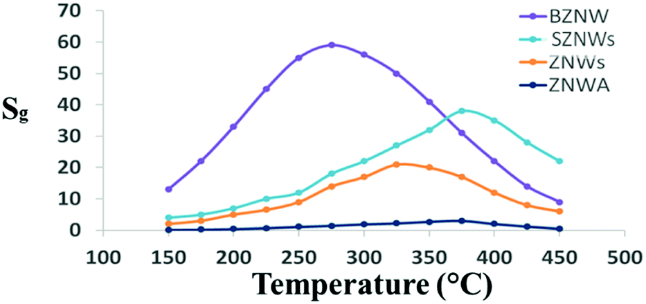 | ||
| Fig. 2 GS response vs. operating temperature curves of the four sensors at an acetone concentration of 200 ppm. | ||
Fig. 3(a) and (b) present the schematic and the sensitivity characteristics of the ZNWA GS, respectively. The sensor response to 200 ppm of acetone gas at 375 °C is about 2.7. The sensor took around 42 s to respond and reach 90% of its maximum value and 56 s to recover to 10% of its original state. The ZNWA GS structure is based on two gold electrodes connected by the seed layer under the ZNWA. This ZnO seed layer is a polycrystalline thin film with ZnO nanoparticles ranging between (300–400 nm) in size. The device response (the ratio of Ig to Ia) is stable, but the sensitivity is low with relatively long response and recovery times. The stability we are referring to here is the ability of the ZNWA GS to generate this value every cycle. The increasing offset after each sensing period of the ZNWA GS could be a result of trapped gas residuals on its surface. The only solution we could think of at this stage is to give it more time to allow the current to come back to its starting level (Ia), and this process may take a very long time. Furthermore, there is a disadvantage in the fabrication procedure; the seed-layer required to be annealed at a relatively high temperature (400 °C), which prevents the use of flexible substrates.
 | ||
| Fig. 3 (a) A schematic diagram and (b) the gas sensing characteristics of the ZNWA sensor to 200 ppm of acetone operated at 375 °°C. | ||
The SZNW GS was also tested at its optimum operating temperature. A schematic diagram and gas sensing characteristics of the SZNWs GS are shown in Fig. 4(a) and (b), respectively. The sensitivity of this device to acetone has been significantly improved relative to the previous ZNWA sensor. The device response to 200 ppm concentration of acetone is about 26 as shown in Fig. 4(b). The response time and recovery-time are 6 and 8 s, respectively. The improvement in the performance of the SZNW sensor over the ZNWA sensor was anticipated because of the reduced size of the active sensing part in the SZNW GS and the increased surface to volume ratio.18
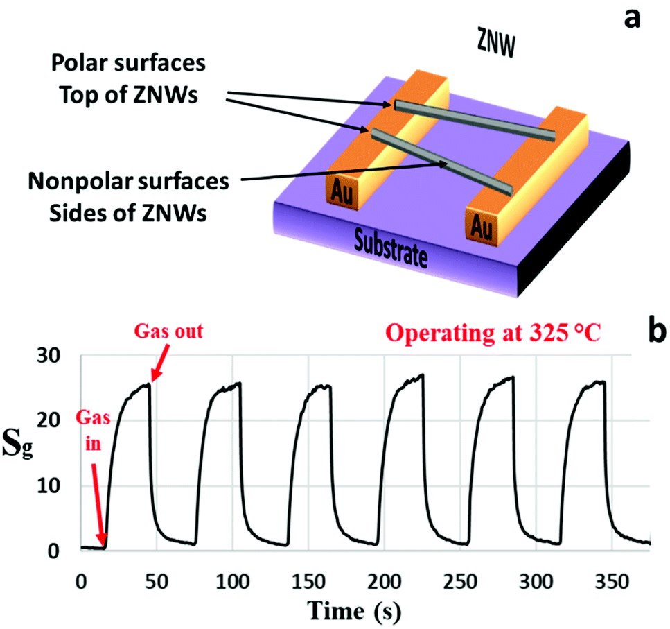 | ||
| Fig. 4 (a) A schematic diagram and (b) the response characteristics of the SZNW sensor to 200 ppm acetone gas operated at 325 °C. | ||
Another nanostructured ZnO GS was fabricated based on the ZNDs, which have different morphology. A schematic diagram, and the gas sensing characteristics of the ZNDs GS are presented in Fig. 5(a) and (b), respectively. The sensitivity of this GS to acetone has been further improved in comparison to the previous ZNWA and SZNW GSs. At its optimum operating temperature, the response to 200 ppm concentration of acetone is about 38, and the response time and recovery time are 11 and 13 s, respectively. The enhancement in this device performance over the ZNWA and SZNW GSs was anticipated due to the increased proportion of the exposed polar facets of the ZND over the other 1D nanostructures. The oxygen ion and gas molecule absorption capability depends greatly on the surface atomic structures. ZnO polar facets, that are terminated with the positive Zn2+ ions, attract atmospheric oxygen (O2) better because of unsaturated oxygen coordination.15 Different surface analysis techniques including Photoluminescence (PL) spectroscopy and X-ray photoelectron spectroscopy (XPS) (not shown here) performed previously support this conclusion. This is a clear example of the possible impact of the morphology and structure on the gas sensing properties of the ZnO nanostructured GSs.25–27
 | ||
| Fig. 5 (a) A schematic diagram and (b) the response characteristics of the ZND sensor to 200 ppm acetone gas operated at 375 °C. | ||
One of our goals in this work is to improve the device structure efficiency to enhance its performance and fabricate it on flexible and transparent substrates. In order to reach these goals, we must be able to achieve the following: (1) create better contact between the ZNWs and the electrodes by growing the ZNWs on the pre-patterned electrodes without any seed layer in between, (2) control the charge transport more efficiently by creating a ZNW–ZNW junction since the impact of gas presence at the potential barrier is the highest, and (3) reduce the size of the active sensing material.
To achieve our goals, our hydrothermal growth technique was modified to allow the growth of ZNWs directly and selectively on the pre-patterned Au electrodes as shown in the SEM images in Fig. 6. These ZNWs are grown directly on the electrodes without the need for a seed layer. The growth solution consisted of Zn(NO3)2·6H2O (25 mM), HMTA (12.5 mM), and NH3·H2O (0.35 M).
 | ||
| Fig. 6 (a)–(d) SEM images at different magnifications of ZNWs grown on prepatterned Au electrodes on a Si/SiO2 substrate. | ||
From our previous studies and the literature,22–24 increasing the concentration of ammonium hydroxide in the growth solution improves the heterogeneous nucleation of ZnO on Au surfaces and consequently the ZNW density at the expense of a slow growth process. However, including PEI can help accelerate and improve the ZNW growth. Nevertheless, we found out that including PEI in the growth solution from the beginning of the growth process prevents any nucleation and disrupts the whole growth process.22–24 Thus, we decided to add PEI gradually after 30 min from the beginning of the growth process to allow the nucleation to occur.
The modified hydrothermal synthesis technique was applied to fabricate BZNW GSs on a substrate. The SEM images at different magnifications of the BZNW GS are presented in Fig. 7 showing nano-junctions created between the BZNWs. A schematic and the gas sensing performance characteristics are presented in Fig. 7(e) and (f), respectively. The sensor response to 200 ppm acetone is around 63. The response-time and the recovery-time of the BZNW GS are 0.42 and 0.90 s, respectively. It is 105, 15, and 26 times faster than the ZNWA, SZNW, and ZND GSs, respectively. The enhancement in the BZNW sensor performance stems from several factors including the more efficient device structure with nano-junctions between the BZNWs and the stronger contact between them and the electrodes.
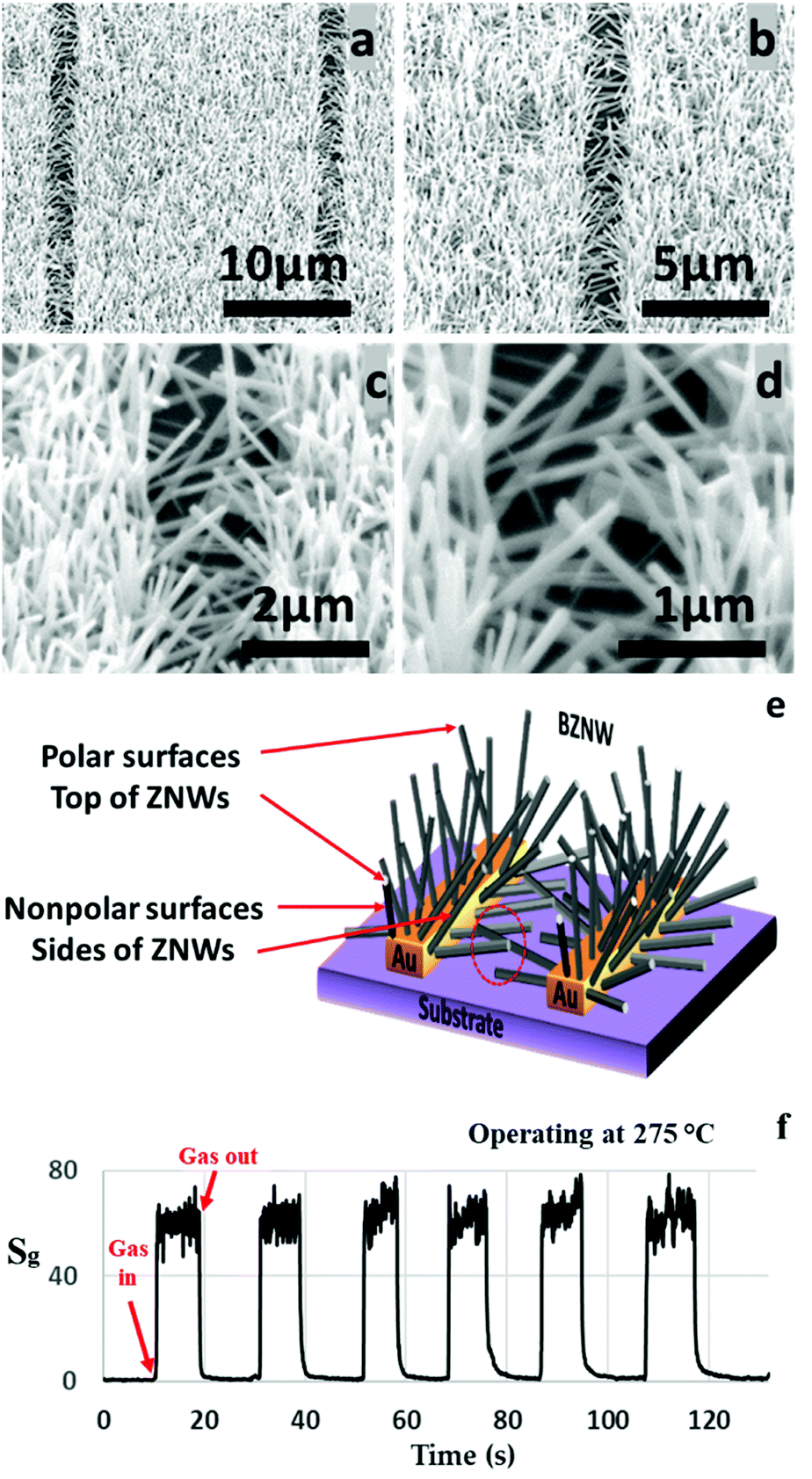 | ||
| Fig. 7 (a)–(d) SEM images at different magnifications, (e) response characteristics of the BZNW sensor operated at 275 °C, and (f) a schematic diagram. | ||
One advantage of our fabrication method is the ability to modify the growth solution during the growth process to design and control the morphology of the final products. For example, in the fabrication process of the BZNW GS described previously, we delayed the introduction of the capping agent PEI to the growth solution by 30 minutes to allow the heterogeneous nucleation of the initial ZNWs on the pre-patterned Au electrodes to occur. Similarly, here we decided to alter the concentrations of the growth solution and the PEI in the second growth phase to control the density and reduce the diameter of the BZNWs, respectively. In fact, we were able to transform the shape of the grown ZNWs into ZNNs with a 20–40 nm diameter as shown in the SEM image in Fig. 8(a). On the other hand, the length of the ZNNs was controlled by the growth time. Fig. 8(b) and (c) present the SEM images of the BZNN GS where ZNNs are connected from both sides and create nano-junctions between them. Due to the influence of the operating temperature on the performance of GSs, the BZNN GS was tested at different temperatures in order to find its optimum operating temperature. However, the performance was not what we expected since the sensitivity is supposed to show a substantial increase as the nanostructure size approaches the Debye length.18 The sensitivity of the BZNN GS was relatively too low. Nevertheless, it was noticed that at lower operating temperature, the sensitivity was much higher than at higher temperatures. So, we decided to expand the operating temperature range and test the BZNN GS at room temperature, where it was higher than all the other tested GSs in this study. A schematic and the performance characteristics of the BZNN GS are shown in Fig. 8(d) and (e), respectively. The GS response to 200 ppm acetone is around 94. The response-time and the recovery-time of the BZNW GS are 81 and 236 s, respectively. Fig. 8(f) compares the sensitivity values of the different fabricated GSs as a function of gas concentration. The order of sensitivities was as follows: BZNNs > BZNWs > ZNDs > SZNWs > ZNWA along the whole concentration range. The BZNN sensor was the most sensitive, while the ZNWA sensor displayed the lowest sensitivity. When the concentration of acetone exceeded 900 ppm, all sensors started to show a sign of saturation at different levels.
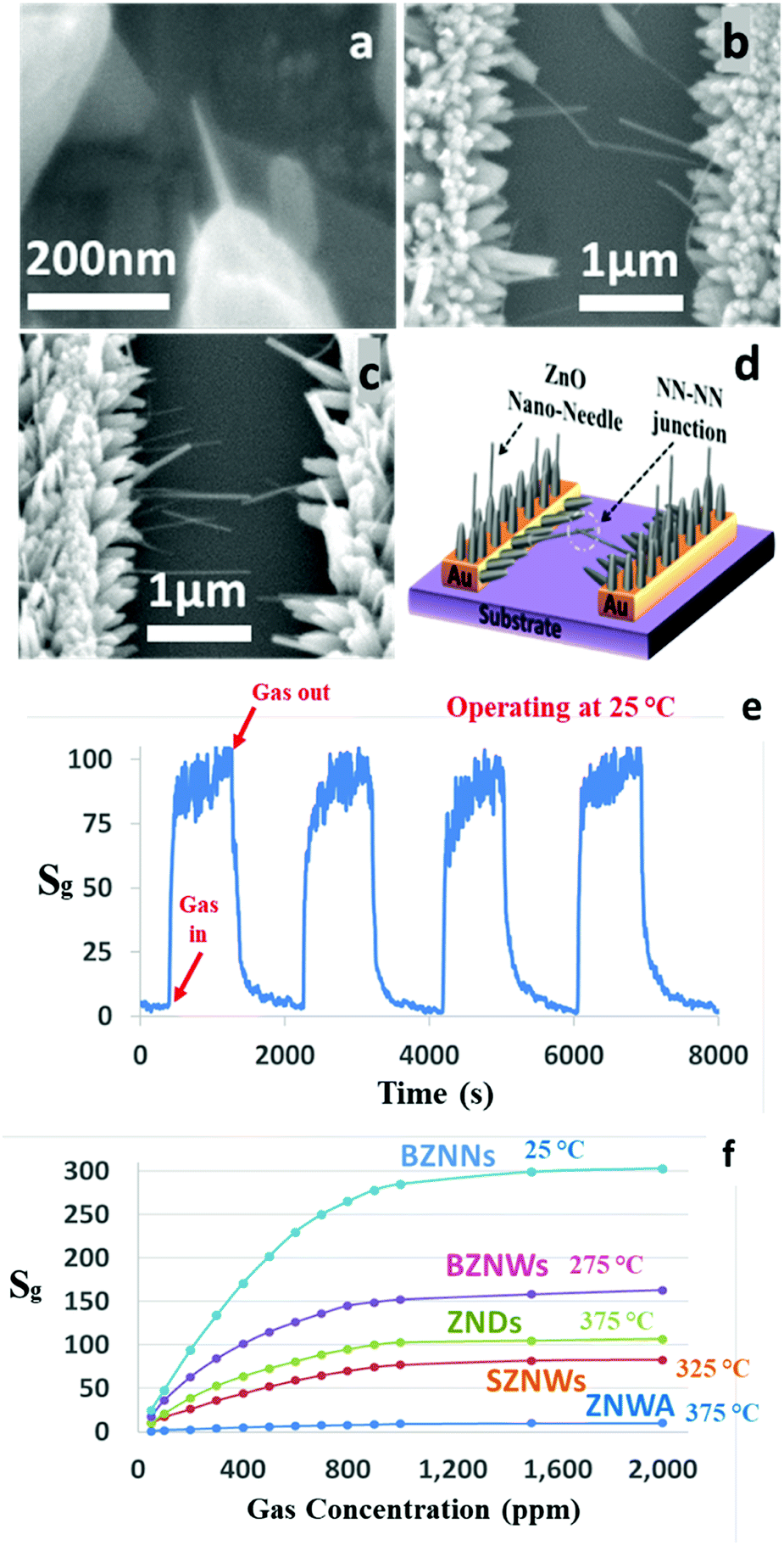 | ||
| Fig. 8 (a) A high magnification SEM image of a single ZNN, (b) and (c) SEM images of BZNNs, (d) a schematic diagram of the BZNN sensor, (e) response characteristics of the BZNN sensor operated at 25 °C, and (f) sensor response as a function of acetone concentration of the five GSs. | ||
Gas molecule adsorption and desorption on the surface of ZnO nanostructures at the required operating temperature may cause an intense change in their electrical conductivity depending on their size and exposed facets, and this represents the basis of the sensing mechanism of ZnO nanostructures. The schematics in Fig. 9 explain and compare charge generation and transportation in the SZNW, BZNW, and BZNN GSs. The schematics explain the sensing mechanism of ZnO nanostructures by the depletion region modulation model.28,29 At room temperature in ambient air, oxygen species are adsorbed on the surface of the ZnO, which is considered as an n-type semiconductor due to the presence of oxygen vacancies (VO) that donate electrons to its conduction band. In the cases of a ZNWA, ZNDs, and SZNWs, the oxygen species on their surfaces attract free electrons from the conduction band and become chemisorbed oxygen species as shown in the first rows of Fig. 9(A)–(C). Depending on the operating temperature, there are different oxygen species including molecular (O2−) and atomic (O− and O2−) ions on the surface. The attraction and capture of the conduction band free electrons expands the depletion layer width near the surface. Subsequently, the conductivity of the nanostructure is reduced greatly as represented in the second rows of Fig. 9(A)–(C). Once acetone gas molecules enter the gas chamber as shown in the third rows of Fig. 9(A)–(C), they participate in oxidation reactions with the chemisorbed oxygen species on the surface and release captured electrons back to the conduction band. The reaction is summarized in eqn (1):30
| CH3COCH3 + 8O(ads)− ⇔ 3CO2 + 3H2O + 8e− | (1) |
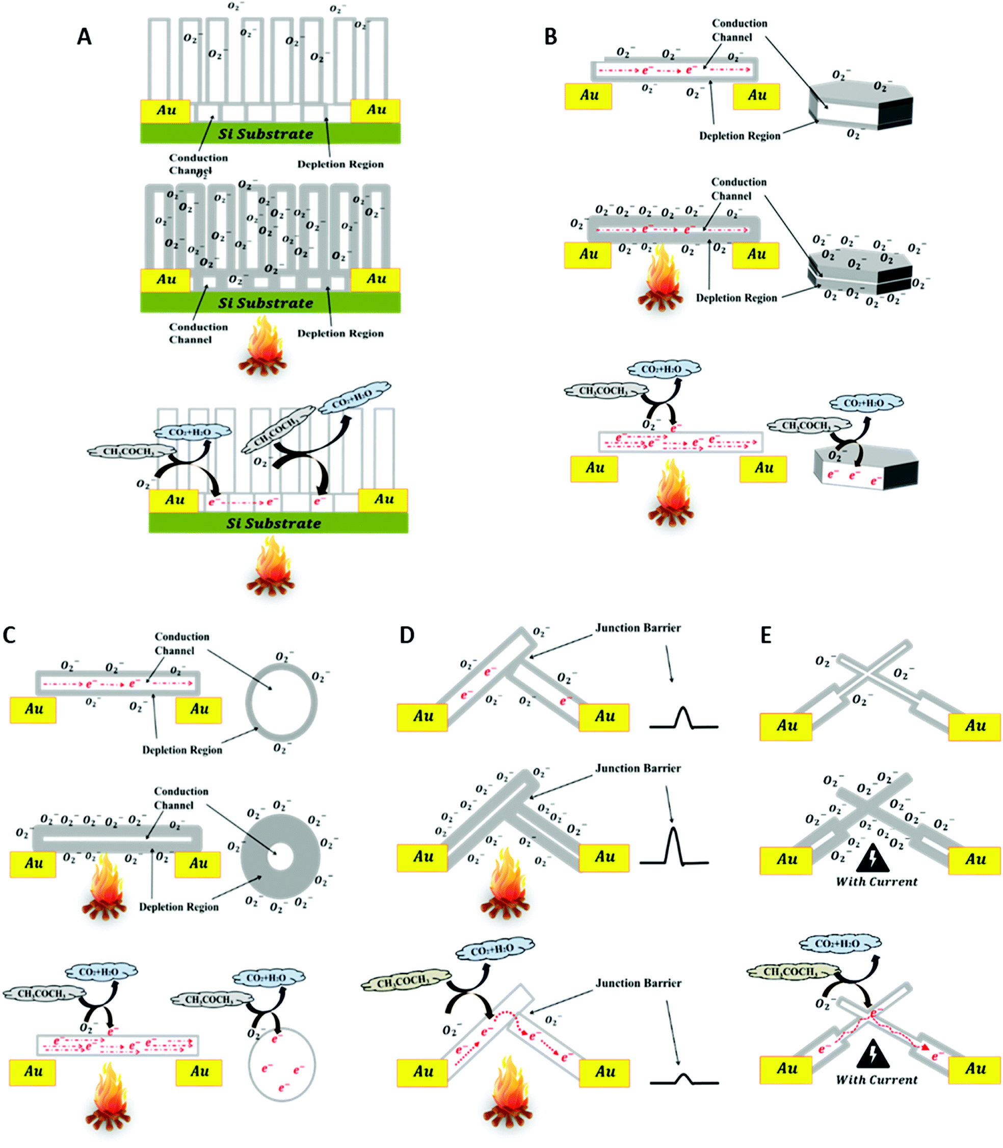 | ||
| Fig. 9 A schematic diagram explaining the sensing mechanism of the (A) ZNWA GS, (B) ZND GS, (C) SZNW GS, (D) BZNW GS, and BZNN GS. | ||
This oxidation process decreases the width of the depletion layer near the surface of the SZNW enhancing its conductivity. Upon gas expulsion and air refreshing in the gas chamber, the oxygen molecules are re-adsorbed on the SZNW surface. As a result, electrons are recaptured, the depletion layer is widened, and the conductivity of the SZNW is reduced again. The conductance of the SZNW can be expressed as:
| G = n0eμπ(D − 2tc)/4l | (2) |
| tc = LD(eVS/kT)1/2 | (3) |
| LD = (εε0kT/e2n0)1/2 | (4) |
Importantly, the conductivity of the BZNW GS is controlled by a mechanism that does not exist in the SZNW GS, since the former conduction channel contains nano-junctions between the BZNWs. As a result, the electrons are required to overcome the junction barrier to allow a current to flow. These barriers are formed by the surface depletion layers of the BZNWs. Thus, for BZNWs with diameters greater than the Debye length, the major modulator of charge flow in the sensors is the junction between the BZNWs as shown in Fig. 9(D). The improvement in its response-time and recovery-time can be ascribed mainly to the domination of the ZNW–ZNW junction barrier over the charge transport. The conductance of the BZNWs GS is controlled more efficiently by the ZNW–ZNW junction barriers, where the flow of charges across the junction barrier is exponentially related to the barrier height, causing the flow of charges to be very sensitive to changes in the barrier. On the other hand, oxygen diffusion and adsorption again to deplete the SZNW channel takes a relatively long time. Consequently, if the GS conductance is controlled by the SZNW conductance only, then it will take too long for the charge to recover. Moreover, the creation of these junctions between the BZNWs may be the reason behind the lower operating temperature of the BZNW GS in comparison with the other GSs. The dissipating heat from the electrical current passing through the ZNW–ZNW junction may have contributed to the activation of the BZNW GS.
Metal oxide GSs require activation thermal energy, and they normally operate at relatively high temperatures (200–400 °C) which are usually provided by external heating sources. However, the BZNN GS was operated at room temperature without any external heating source. The activation thermal energy needed to operate was generated by the dissipating heat from the electrical current passing in the ZNNs that have dimensions comparable to the Debye length as shown in the second row of Fig. 9(E). This intense reduction in dimensionality of the ZNNs allowed a complete depletion of the ZNNs minimizing the influence of the nano-junctions between the BZNNs on the BZNN GS conductivity. Subsequently, the sensitivity of the BZNN GS improved substantially, and the response and recovery times increased in comparison with the other tested GSs.
Conclusions
We herein report the successful development of a facile, cost-effective, seedless, and position-selective hydrothermal synthesis technique for the fabrication of high-performance ZnO nanostructured gas sensors (GSs) on a substrate. The ability to rationally control the morphology and structure of the produced nanostructure was demonstrated by tuning the experimental parameters employed during the growth process. Furthermore, the efficiency of the fabricated device structure was improved and subsequently enhanced its performance substantially. Compared to other fabricated nanostructured ZnO GSs, the on-substrate fabricated BZNN GS demonstrated superior sensitivity (∼94) and self-activation, which were attributed to the unique ZNN–ZNN junction barrier dominated resistance and the direct contact between ZnO and Au electrodes, and the reduction in the sensing material dimensions as well as the ultrahigh surface-to-volume ratio. This work paves the way for low cost, large scale, low temperature, seedless and position-selective fabrication of high-performance self-activated nanostructured metal oxide GSs on flexible and transparent substrates.Experimental details
The reagents in this work are analytical grade. For the synthesis of the ZNWA, a silicon (Si) substrate was spin coated with zinc acetate solution and cured at 400 °C for 30 minutes to form a seed layer on it. The Si substrate was an n-doped Si wafer (150 mm thick) covered with a SiO2 layer (230 nm ± 10 nm thick). The prepatterned electrodes were composed of a 30 nm Au layer on top of a 10 nm high work function adhesion layer. The coated substrate was then immersed in a vial of a growth solution of 25 mM zinc nitrate, 12.5 mM hexamethylenetetramine (HMTA), 0.35 M ammonium hydroxide, and 5 mM polyethylenimine (PEI, end-capped, molecular weight 800 g per mol LS, Aldrich).Afterwards, the vial was sealed and heated in an oven at 90 °C for 24 hours. Upon growth termination, the substrate was washed with water and dried at 150 °C for 30 min. In order to get a suspension of isolated SZNWs, ZNWA was placed in a DI water vial and was vibrated in an ultrasonic bath.
For the reparation of the ZNDs, the growth solution was a mixture of 100 mM zinc sulphate (ZnSO4) and 100 mM HMTA. The growth solution was heated in an oven at 75 °C for 3 hours. The prepared ZNDs were filtered and washed with DI water.
ZNWA, SZNW, and ZND GSs were fabricated for comparison. SZNW and ZND GSs were fabricated by drop casting a solution containing ZNWs and ZNDS, respectively, on substrates with Au pre-patterned electrodes. The substrates were annealed at 200 °C for 2 h for better contact between the ZNWs and ZNDs and the electrodes.
The morphology and crystal structure analysis of the grown ZnO nanostructures was performed by scanning electron microscopy (SEM) using a Philips XL-20 microscope at 10 kV. The crystal structure analysis of the grown ZnO nanostructures was performed by powder X-ray diffraction (XRD) using a Panalytical X'Pert diffractometer with Cu Kα radiation. Scanning transmission electron microscopy (STEM) and electron diffraction analyses were performed using a Hitachi HD2300A microscope, operating at 200 kV.
The electrical conductivity of the prepared nanostructured GSs was observed by using a Keithley 4200 semiconductor analyzer with a probe station. The GS response, Sg, is defined as Sg = (Ig − Ia)/Ia, where Ig and Ia are the GS current values in gas and pure air environments, respectively. The response time, tr, is the time needed for the current to reach 90% of the equilibrium value after the tested gas is injected. On the other hand, the recovery time, td, is the time needed for the current to return to 10% of the equilibrium current value in fresh air after releasing the gas from the gas chamber.
Conflicts of interest
There are no conflicts to declare.Notes and references
- Z. Wang, J. Gong, Y. Su, Y. Jiang and S. Yang, Six-Fold-Symmetrical Hierarchical ZnO Nanostructure Arrays: Synthesis, Characterization, and Field Emission Properties, Cryst. Growth Des., 2010, 10, 2455–2459 CrossRef CAS.
- C. S. Lao, et al., Giant Enhancement in UV Response of ZnO Nanobelts by Polymer Surface-Functionalization, J. Am. Chem. Soc., 2007, 129, 12096–12097 CrossRef CAS PubMed.
- J. B. K. Law and J. T. L. Thong, Simple fabrication of a ZnO nanowire photodetector with a fast photoresponse time, Appl. Phys. Lett., 2006, 88, 133114 CrossRef.
- H. E. Unalan, et al., Zinc oxide nanowire networks for macroelectronic devices, Appl. Phys. Lett., 2009, 94, 163501 CrossRef.
- M. R. Alenezi, S. J. Henley and S. R. P. Silva, On-chip Fabrication of High Performance Nanostructured ZnO UV Detectors, Sci. Rep., 2015, 5, 8516 CrossRef PubMed.
- M. R. Alenezi, A. S. Alshammari, P. D. Jarowski, T. H. Alzanki, S. J. Henley and S. R. P. Silva, ZnO nanodisk based UV detectors with printed electrodes, Langmuir, 2014, 30, 3913–3921 CrossRef CAS PubMed.
- D. Shakthivel, R. S. Dahiya, M. Ahmad, M. R. Alenezi and S. R. P. Silva, 1D Semiconducting Nanostructures for Flexible and Large-Area Electronics, Cambridge University Press, 2019 Search PubMed.
- M. R. Alenezi, UV Sensor Based on Single Metal Oxide Nanowire, Int. J. Eng. Res. Technol., 2014, 7, 755–758 Search PubMed.
- X. Zhou, Z. X. Xie, Z. Y. Jiang, Q. Kuang, S. H. Zhang, T. Xu, R. B. Huang and L. S. Zheng, Formation of ZnO hexagonal micro-pyramids: a successful control of the exposed polar surfaces with the assistance of an ionic liquid, Chem. Commun., 2005, 5572–5574 RSC.
- C. Wang, L. Yin, L. Zhang, D. Xiang and R. Gao, Metal oxide gas sensors: sensitivity and influencing factors, Sensors, 2010, 10(3), 2088–2106 CrossRef CAS PubMed.
- Y.-F. Sun, S.-B. Liu, F.-L. Meng, J.-Y. Liu, Z. Jin, L.-T. Kong and J.-H. Liu, Metal Oxide Nanostructures and Their Gas Sensing Properties: A Review, Sensors, 2012, 12(3), 2610–2631 CrossRef CAS PubMed.
- S. Capone, A. Forleo, L. Francioso, R. Rella, P. Siciliano, J. Spadavecchia, D. S. Presicce and A. M. Taurino, Solid state gas sensors state of the art and future activities, J. Optoelectron. Adv. Mater., 2003, 5, 1335–1348 CAS.
- N. Al-Hardan, M. J. Abdullah and A. Abdul Aziz, The gas response enhancement from ZnO film for H2 gas detection, Appl. Surf. Sci., 2009, 255, 7794–7797 CrossRef CAS.
- S. Salehi, E. Nikan, A. A. Khodadadi and Y. Mortazavi, Highly sensitive carbon nanotubes–SnO2 nanocomposite sensor for acetone detection in diabetes mellitus breath, Sens. Actuators, B, 2014, 205, 261–267 CrossRef CAS.
- M. R. Alenezi, S. J. Henley, N. G. Emerson and S. R. P. Silva, From 1D and 2D ZnO nanostructures to 3D hierarchical structures with enhanced gas sensing properties, Nanoscale, 2014, 6, 235–247 RSC.
- M. R. Alenezi, A. S. Alshammari, K. D. G. I. Jayawardena, M. J. Beliatis, S. J. Henley and S. R. P. Silva, Role of the exposed polar facets in the performance of thermally and UV activated ZnO nanostructured gas sensors, J. Phys. Chem. C, 2013, 117, 17850–17858 CrossRef CAS PubMed.
- R. A. Mohammad, Hierarchical zinc oxide nanorings with superior sensing properties, Mater. Sci. Eng., B, 2018, 236–237, 132–138 Search PubMed.
- M. R. Alenezi, T. H. Alzanki, A. M. Almeshal, A. S. Alshammari, M. J. Beliatis, S. J. Henley and S. R. P. Silva, A model for the impact of the nanostructure size on its gas sensing properties, RSC Adv., 2015, 5, 103195 RSC.
- J. D. Prades, R. Jimenez-Diaz, F. Hernandez-Ramirez, S. Barth, A. Cirera, A. Romano-Rodriguez, S. Mathur and J. R. Morante, Ultralow power consumption gas sensors based on self-heated individual nanowires, Appl. Phys. Lett., 2008, 93, 123110 CrossRef.
- J. G. Strom and H. W. Jun, Kinetics of hydrolysis of methenamine, J. Pharm. Sci., 1980, 69, 1261–1263 CrossRef CAS PubMed.
- K. Govender, D. S. Boyle, P. B. Kenway and P. O'Brien, Understanding the factors that govern the deposition and morphology of thin films of ZnO from aqueous solution, J. Mater. Chem., 2004, 14, 2575–2591 RSC.
- C. K. Xu, P. Shin, L. L. Cao and D. Gao, Preferential Growth of Long ZnO Nanowire Array and Its Application in Dye-Sensitized Solar Cells, J. Phys. Chem. C, 2010, 114, 125–212 CrossRef CAS.
- J.-H. Tian, J. Hu, S.-S. Li, F. Zhang, J. Liu, J. Shi, X. Li, Z.-Q. Tian and Y. Chen, Improved seedless hydrothermal synthesis of dense and ultralong ZnO nanowires, Nanotechnology, 2011, 22, 245601 CrossRef PubMed.
- R. Parize, J. D. Garnier, E. Appert, O. Chaix-Pluchery and C. Vincent, Effects of Polyethylenimine and Its Molecular Weight on the Chemical Bath Deposition of ZnO Nanowires, ACS Omega, 2018, 3(10), 12457–12464 CrossRef CAS PubMed.
- W. Kim, M. Choi and K. Yong, Generation of oxygen vacancies in ZnO nanorods/films and their effects on gas sensing properties, Sens. Actuators, B, 2015, 209, 989–996 CrossRef CAS.
- Z. H. Jing and J. H. Zhan, Fabrication and Gas-Sensing Properties of Porous ZnO Nanoplates, Adv. Mater., 2008, 20, 4547–4551 CrossRef CAS.
- X.-G. Han, H.-Z. He, K. Qin, X. Zhou, X.-H. Zhang, T. Xu, Z.-X. Xie and L.-S. Zheng, Controlling morphologies and tuning the related properties of nano/microstructured ZnO crystallites, J. Phys. Chem. C, 2009, 113, 584–589 CrossRef CAS.
- L. Liao, H. B. Lu, J. C. Li, H. He, D. F. Wang, D. J. Fu, C. Liu and W. F. Zhang, Size dependence of gas sensitivity of ZnO nanorods, J. Phys. Chem. C, 2007, 111, 1900–1903 CrossRef CAS.
- A. Gurlo, Nanosensors: towards morphological control of gas sensing activity. SnO2, In2O3, ZnO and WO3 case studies, Nanoscale, 2011, 3, 154–165 RSC.
- P. A. Murade, V. S. Sangawar, G. N. Chaudhari, V. D. Kapse and A. U. Bajpeyee, Gas sensing performance of nanocrystalline ZnO prepared by a simple route, Curr. Appl. Phys., 2010, 11, 451–456 CrossRef.
- V. V. Sysoev, B. K. Button, K. Wepsiec, S. Dmitriev and A. Kolmakov, Toward the Nanoscopic “Electronic Nose”: Hydrogen vs. Carbon Monoxide Discrimination with an Array of Individual Metal Oxide Nano- and Mesowire Sensors, Nano Lett., 2006, 6, 1584–1588 CrossRef CAS PubMed.
| This journal is © The Royal Society of Chemistry 2022 |