
 Open Access Article
 This Open Access Article is licensed under a Creative Commons Attribution-Non Commercial 3.0 Unported Licence
In situ tunable circular dichroism of flexible chiral metasurfaces composed of plasmonic nanorod trimers†
Hsiang-Ting
Lin
 a,
Yao-Yu
Hsu
ab,
Pi-Ju
Cheng
a,
Wei-Ting
Wang
a,
Shu-Wei
Chang
ab and
Min-Hsiung
Shih
*abc
a,
Yao-Yu
Hsu
ab,
Pi-Ju
Cheng
a,
Wei-Ting
Wang
a,
Shu-Wei
Chang
ab and
Min-Hsiung
Shih
*abc
aResearch Center for Applied Sciences, Academia Sinica, Taipei 11529, Taiwan. E-mail: mhshih@gate.sinica.edu.tw
bDepartment of Photonics and Institute of Electro-Optical Engineering, National Yang Ming Chiao Tung University, Hsinchu 30010, Taiwan
cDepartment of Photonics, National Sun Yat-sen University, Kaohsiung 80424, Taiwan
First published on 14th March 2022
Abstract
The circularly polarized light source is one of the keys to chiral photonic circuits and systems. However, it is difficult to integrate conventional light-emitting devices with circular polarization converters directly into compact chip-scale photonic systems partly because of their bulky structures. In this study, in situ optical chirality tunable nanorod trimer metasurfaces consisting of two types of nanorod dimers are demonstrated and integrated with a flexible polydimethylsiloxane (PDMS) substrate. The optical chirality variations originating from the tunable asymmetricity of nanorod trimers under different stretching scenarios are evaluated. Through the processes, the gap distances between nanorods are varied, and the degree of circular polarization of the transmitted wave is controlled through the manipulation of localized surface plasmon resonance (LSPR) coupling. The results reveal the circular dichroism tunability and durability of fabricated chiral metasurfaces which can be important elements for chip-scale flexible optoelectronic integrated circuits for sensing, display and communication applications.
Introduction
Circularly polarized (CP) light and the chiroptical effect have received considerable attention in advanced optoelectronic technologies and relevant applications, including optical spintronics,1,2 quantum optical communication/information processing,3–5 and backlighting of high-efficiency liquid crystal display.6,7 Moreover, reliable methods to manipulate CP light states and circular dichroism (CD) spectroscopy have also played important roles in various applications involving optically active molecules,8–11 chiral synthesis12–14 in biology and chemistry, and ultrafast magnetization control.15,16 However, conventional CP light generating and controlling methods rely on the bulky circular polarization converter and are difficult to integrate directly into compact chip-scale photonic systems. In order to control the CP light more efficiently, compact CP light tunable devices are critical for improving chiral photonic systems.Metasurfaces are planar photonic nanostructures with subwavelength thicknesses. They can support specifically designed optical wave fronts for certain unique functionalities which had been regarded as merely realizable by bulk optical components in the past.17,18 For example, functions of conventional lenses and prisms rely on field interference or phase accumulation during wave propagation in media. In contrast, those of the metasurface are realized by hybridizing the modal fields and engineering the phases of each nanoscale element on it. The local phase can be designed by manipulating the shape,19 size,20 or geometrical orientation of each element. Many metasurface devices have been developed for various purposes, including analogies to refraction and diffraction in Snell's law,21–24 optical lenses,25–29 optical polarization control,30–39 optical vortices40–43 and optical sensors.44–49 In this study, we realized a tunable, reversible chiroptical metasurface integrated with a flexible polydimethylsiloxane (PDMS) substrate. In recent studies, the optical characteristics of flexible metasurfaces have been tuned through the stretching or bending of devices.50–56 Here, with the high flexibility of PDMS, the localized surface plasmon resonance (LSPR) coupling in the designed metasurfaces was carefully controlled through device stretching. Furthermore, the degree of CP of transmitted light was efficiently manipulated with a wide tuning range of CD.
Results and discussion
Fig. 1a shows the schematics of a gold (Au) nanorod trimer metasurface and the PDMS substrate. The array of Au nanorod trimers were embedded in the flexible substrate, which could be stretched to tune the gap and period of the metasurface. Through the bonding method, we successfully transferred the metasurface from the indium phosphide (InP) sacrificial substrate (as shown in Fig. 1b) to the flexible PDMS substrate (the fabrication details are described in Section S1 of the ESI†). The metasurfaces are composed of three identical nanorods of which the length (L), width (W), and height (H) are 210, 100, and 50 nm, respectively. In the presence of stretching, the asymmetric coupling strength and phase differences between the localized surface plasmon waves around the metallic nanorods played critical roles in inducing optical chirality.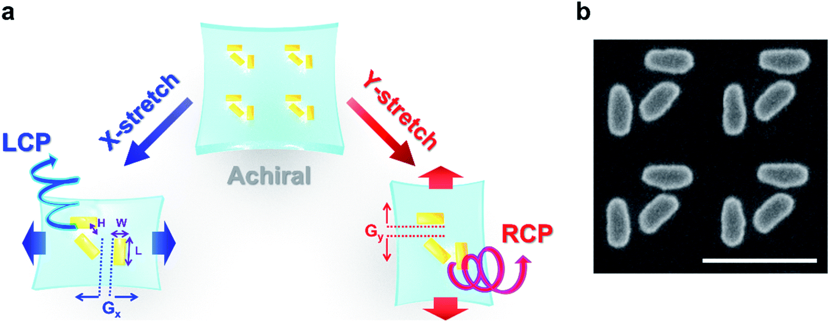 | ||
| Fig. 1 (a) Illustrations of the optical chirality tunable Au nanorod trimer metasurface on the flexible and stretchable PDMS substrate. (b)The SEM image of the Au nanorod trimer metasurface. The dimensions of the nanorods are L = 210 nm, W = 100 nm, and H = 50 nm. The scale bars are 500 nm. | ||
To investigate the origin of CD tunability in our fabricated metasurfaces, the nanorod trimer was deconstructed into two sets of nanorod dimers, as shown in Fig. 2a. The two dimers, denoted as D+ and D−, were mirror images of each other and had identical dimensions but different orientations. In each dimer, the small gaps between nanorods resulted in strong LSPR coupling. Fig. 2b displays the extinction spectrum of D+ dimers alone using the 3-D finite-difference time-domain (FDTD) method. Several peaks originating from different resonance couplings between the long-axis and short-axis LSPR modes of nanorods are observable. Owing to the specific arrangement of nanorod dimers, the coupling between long-axis LSPR modes at approximately 854 nm was dominant. Fig. 2c shows the calculated field profiles of the D+ dimer under the RCP and LCP incidences. The near-field squared magnitude of electric field |E|2 under the RCP incidence is much more localized in the gap than that under the LCP incidence. These distinct near-field profiles under incident fields with opposite handedness lead to the far-field optical chirality and CD of the dimer structure.
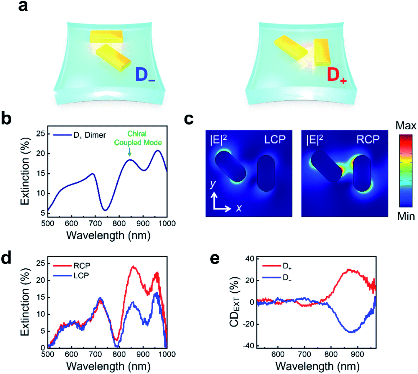 | ||
| Fig. 2 (a) Illustrations of the right-handed dimer (D+) and the left-handed dimer (D−). (b) Calculated spectrum of the right-handed (D+) dimer nanostructure, and (c) the field profiles of the chiral coupled mode at 854 nm. (d) The RCP (red) and LCP (blue) resolved extinction spectra of the fabricated right-handed dimer (D+) metasurface. (e) The extinction CD spectra of the right-handed dimer (D+) and the left-handed dimer (D−) metasurfaces. | ||
We further investigated the far-field optical properties of the D+ and D− dimers, respectively. The metasurfaces composed of either D+ or D− nanorod dimers embedded in PDMS were fabricated through the same procedure as that for trimers. And the extinction spectra of CP light were characterized using a microscope-based extinction measurement system. The details of optical measurement are provided in Section S2 of the ESI.†Fig. 2d shows the left-handed CP (LCP) and right-handed CP (RCP) extinction spectra of the D+ dimers. The wavelengths of multiple extinction peaks in the spectra match simulation predictions. Moreover, the significant differences between the LCP and RCP extinction spectra from 800 to 1000 nm were indicative of strong optical chirality. To quantify the optical chirality, we further calculated the CD of extinction as follows:
 | (1) |
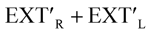 is the sum magnitude at the extinction peak around 858 nm for normalizing the CDEXT magnitude.38,57,58Fig. 2e exhibits the corresponding CDEXT of the D+ and D− dimer metasurfaces. The significant extinction differences between EXTR and EXTL are manifested as peaks (dips) in the CDEXT spectra of the D+ (D−) dimers. Notably, the positive (negative) peak (dip) of about 30% or corresponding to about +0.6 (−0.6) of the extinction dissymmetry factor gEXT on the CDEXT spectrum of D+ (D−) dimers reflects the strong coupling with RCP (LCP) light. The metasurface of trimers can be approximated as the combination of two sets of nanorod dimers, which have high optical chirality but opposite inclinations to CP light. The trimer structure also provides us an efficient way to tune the CD. In essence, manipulating the spatial arrangement of nanorods in trimers so that the resonance features of either D+ or D− dimers can stand out is the key to the tunability of CD.
After the chiroptical properties of the dimer metasurfaces were verified, we further investigated those of the trimer structure. Each trimer unit comprised three gold nanorods of identical dimensions. One of the three nanorods was centered in the unit cell with a 45° rotation. The remaining two were arranged at the top and right of the unit cell, separated from the center nanorod by two gaps denoted as Gx and Gy, respectively (see Fig. 1a). The small gaps between the adjacent nanorods are crucial for strong localized plasmon resonances. As the gap distance decreased, the restoring force acting on the oscillating electrons of each nanorod was reduced by the charge distribution of the adjacent nanorod. In other words, the frequency of dipole oscillation along the long axis of nanorods depended on the gap distance, and decreasing this distance redshifted the resonance quasi-exponentially. This result is consistent with previous reports.35,59–61 To investigate the optical chirality of the trimer structures due to this effect, nanorod trimers with different Gx and Gy were fabricated.
The symmetric structural setting was Gx = Gy = 40 nm. As in the case of dimer metasurfaces, the coupling resonances between nanorods lead to multiple extinction peaks in both FDTD calculated and measured extinction spectra as displayed in Fig. S3a and S3b.† The geometric symmetry indicates the achiral response of the coupled LSPR modes which is confirmed by the almost overlapping extinction spectra resolved with opposite CP light shown in Fig. S3b.† The optical chirality emerged as the couplings between the center and side nanorods were asymmetric—that is, Gx < Gy or Gx > Gy. As one of the sided nanorods moved away from the center nanorod, the LSPR coupling began to resemble that of the D+ or D− chiral nanorod dimers, indicating that control of Gx and Gy can be efficiently utilized to manipulate the LSPR modes for the inclination to LCP or RCP lights.
Fig. 3c and d display the CP resolved extinction spectra of trimer metasurfaces with Gx < Gy and Gx > Gy, respectively. As in the case of dimer metasurfaces, multiple extinction peaks are observable. These phenomena are partially due to the resonance coupling between the LSPR modes of the two nanorods which were brought closer.61 However, the remaining nanorod in the trimer structure might still influence the weightings of the two LSPR couplings and hence led to the deviation between the asymmetric trimer metasurfaces and corresponding dimer structures. Regarding the optical chirality, the resonance corresponding to the coupling between the long-axis modes at around 850 nm contributed critically to the CD of transmitted light. Comparing the measured and simulation extinction spectra (shown in Fig. S4a and S4b†) with Gx < Gy and Gx > Gy, we found that the extinction peaks around 850 nm exhibited opposite responses to the LCP and RCP lights, whereas extinctions in other resonant peaks were almost identical for both CP lights. This indicates that the 850 nm resonant mode of the trimer structure with Gx < Gy (Gx > Gy) tended to interact with the RCP (LCP) light and resulted in the stronger EXTR (EXTL).
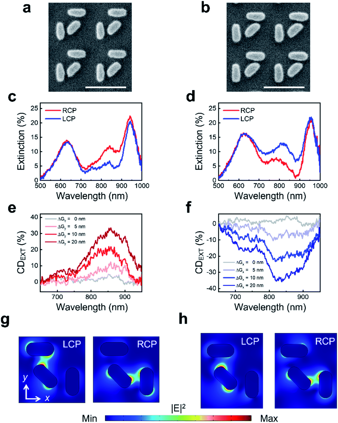 | ||
| Fig. 3 SEM images of the (a) Gx < Gy (Gx = 40 nm; Gy = 60 nm) and (b) Gx > Gy (Gx = 60 nm; Gy = 40 nm) asymmetric nanorod trimers before bonding to the PDMS substrate. The scale bars are 500 nm. Extinction spectra of the trimer metasurface at (c) Gx < Gy as shown in (a), and (d) the counterparts of the trimer metasurface at Gx > Gy as shown in (b). The CD spectra of the trimer metasurface with (e) increasing Gy and (f) increasing Gx. Field profiles of the trimer at (g) Gx = Gy = 40 nm and (h) Gx < Gy under the CP incidence conditions. | ||
We also converted the CP resolved extinction spectra of the fabricated nanorod trimer metasurfaces into the corresponding CDEXT spectrum using eqn (1) for further investigation. Fig. 3e and f show a series of CDEXT spectra corresponding to trimers with varying gap distances for both cases of Gx < Gy and Gx > Gy. In the scenario with Gx < Gy (Gx > Gy), the gap Gx (Gy) was fixed at approximately 40 nm while the other ranged between 45 and 60 nm. As mentioned earlier, the asymmetric coupling featuring distinct Gx and Gy corresponded to different inclinations of LCP and RCP light. This explains the observations of positive peaks on the CDEXT around 850 nm at Gx < Gy but negative ones at Gx > Gy. Moreover, the magnitude |CDEXT| increased with increasing gap distance in the trimers regardless of the cases Gx < Gy or Gx > Gy, indicating a strong optical chirality. For the trimer metasurface presented in this study, the magnitude |CDEXT| ranged from 0 (Gx = Gy) to roughly ±40% or 0 to ±0.8 of gEXT.
To further understand the optical chirality of nanorod trimers, we calculated the profiles of the corresponding electric field through three-dimensional FEM. Fig. 3g displays the distribution of field magnitude around a nanorod trimer at Gx = Gy under the CP incident field. The field profiles in the two CP cases actually look like mirror images of each other. For the RCP (LCP) incident light, an intense local field profile is present around the right (top) gap region. Yet, the two gap regions provide the same amount of absorption and similar polarization conversion for the two CP lights. Consequently, the far-field optical chirality which is mainly characterised by the difference of chiral responses in the two gap regions is absent at Gx = Gy, indicating that these nanorod trimers are achiral. In contrast, at Gx < Gy, the symmetric coupling in the gap regions is broken. The increased gap distance Gy weakens the LSPR coupling in the top gap region. This brings about the unbalanced CP responses around the two gap regions and therefore nonvanishing far-field optical chirality. Moreover, the field distribution of the trimer (Fig. 3h) resembles that around the D+ dimer (Fig. 2c) under the RCP incidence. Their real-time nearfields reveal that the strong confinement of plasmonic modes results in the absorption of the incoming wave and polarization selection (see ESI Movie S1† and the description in Section S4 of the ESI†). Therefore, the trimer in this case exhibits an RCP-preferred chiral response similar to that of the D+ dimer and therefore a positive CDEXT. The optical chirality of the trimer structure depends on the variation in the gap distance rather than the changes in dimensionality or arrangement of nanorods. This picture suggests that if the gap distance can be efficiently manipulated, a device in which in situ tuning and reversal of CD may be realized.
PDMS has been widely applied as a flexible and stretchable platform for the in situ control of various optical properties of nanodevices.50–56 As nanostructures are integrated with a PDMS substrate, the arrangements and distances between each component can be readily tuned on the ten-nanometer scale by stretching or bending the device.51,53 This is especially convenient for tuning optical properties of plasmonic metasurfaces because the LSPR coupling is related to distance variations between nanostructures. The effect also plays an essential role in the in situ tuning of our chiral metasurfaces integrated with a PDMS substrate. As mentioned earlier, by changing the gap distances Gx and Gy in nanorod trimers, different behaviors of CDEXT can be realized. Utilizing the high flexibility of PDMS, we could fine tune the LSPR coupling in nanorod trimers through device stretching and manipulate the circular polarization degree of the incident light extinction with a broad tuning range.
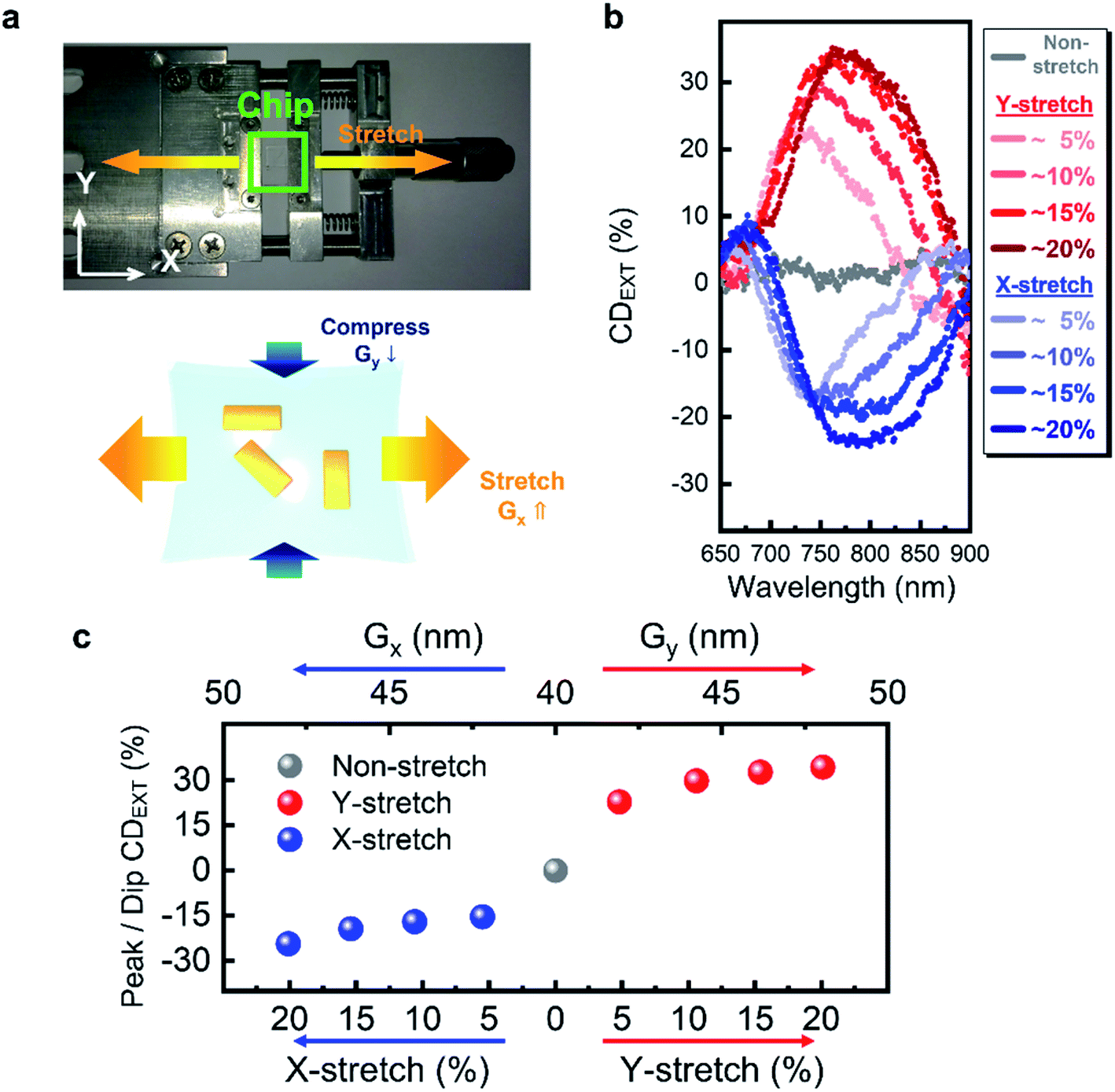
For tuning the optical chirality through mechanical stretching, the chip was mounted on a homemade extension stage as shown in Fig. 4a. Before characterizing the optical properties under stretching, device stretchability should be quantified. We focused on nanorod trimers with identical gap distances Gx = Gy = 40 nm. The effect of stretching the mounted chip was examined, and the relationship between the stretch level of the PDMS substrate and gap distances between nanorods was calibrated. On account of Poisson's ratio of the PDMS substrate, stretching the chip along the x-axis not only increased Gx but also slightly reduced Gy. When the chip was stretched along the y-axis, similar variations in gap distances Gy and Gx were observed. It indicates that the nanorod trimers became more asymmetric under stretching and exhibited variable levels of optical chirality, in accord with the results of previous analysis.
 | ||
| Fig. 4 (a) Flexible chiral metasurface device mounted on a homemade stage. (b) The extinction CD spectra of the chiral trimer metasurface at various stretch levels along the x-axis and the y-axis. (c) The CD magnitude tuning of the trimer metasurface through mechanical stretching. | ||
We investigated the optical chirality of the fabricated nanorod trimer metasurface under different stretch scenarios. Fig. 4b shows the CDEXT spectra of the trimer metasurface in a series of stretch tests. The gray line denotes the baseline conditions of no stretching. Because of the symmetric structure at Gx = Gy, CDEXT almost vanished at various wavelengths, indicating that the baseline structure is achiral. After stretching along the y-axis, positive spectral peaks on CDEXT were detected from 750 to 800 nm. Moreover, the magnitude |CDEXT| increased with the amount of stretch applied. In contrast, as the metasurface is stretched along the x-axis, negative counterparts on |CDEXT| which were proportional to the amount of stretch were also observable. This is attributable to the fact that the stretching along the y (x) axis increased Gy (Gx). At the same time, Gx (Gy) was slightly reduced. Both factors enhanced device asymmetry and raised |CDEXT|. The |CDEXT| variation with stretch is not quite linear which is due to the non-uniform PDMS strain on the nanometer scale. In the series spectra of CDEXT, we observed a redshift in the peaks/dips under stretching; this is attributable to the increase in the period of nanorod trimers as the stretch level increased. Fig. 4c shows the variations of peaks/dips in the spectra of CDEXTversus the amount of stretch applied. When the device was stretched along the y-axis, the CDEXT showed a positive value, which indicates the right-handed circular polarization operation. In contrast, when the device was stretched along the x-axis, the CDEXT showed a negative value, which indicates the left-handed circular polarization operation. The results show that the original achiral metasurface could be actively tuned to induce positive CDEXT with a maximum of approximately +30% as a stretch level of 20% was applied along the y-axis. If the metasurface was stretched along the x-axis, the CDEXT became negative and peaked around −25%. Overall, in one trimer metasurface, a large CDEXT with an active tuning range over 55% was achieved by changing the stretch level and the direction of stretching. For the flexible devices, durability is also an important property which should be considered when assessing the potential of flexible devices for practical applications. We further examined the durability and reliability of our devices by repeating many stretch and release cycles (for details, see Section S5 of the ESI†). It shows that the CD variation of our devices remained less than ±5% during the durability test which represents the high durability and reliability of our chiral metasurface as well as its excellent tunability of CD.
Conclusions
In summary, we have demonstrated optical chirality tunable nanorod trimer metasurfaces on flexible PDMS substrates through mechanical stretching. The plasmonic nanorod trimer comprised two types of chiral nanorod dimers associated with left-handed and right-handed CP lights. Combining the results of near-field simulation and far-field optical characterization of the nanorod trimers, it suggested that manipulating the gap distances between nanorods is the key to strong optical chirality. By integrating the trimer metasurface into flexible PDMS substrates, efficient control over the gap distance and further manipulation of the degree of circular polarization in the LSPR modes on the metasurfaces were realized. With the change in gap distances, CDEXT was tuned from around −25% to +30%, corresponding to a tuning range larger than 55%. Because of its compact footprint, geometrical flexibility, and circular polarization tunability, this metasurface can be further integrated into chip-scale optoelectronic circuits or bio-related sensing systems.Author contributions
Conceptualization: HTL and MHS. Data curation: HTL and YYH. Formal analysis: HTL, WTW, and MHS. Methodology: HTL, PJC, SWC, and MHS. Investigation: HTL and YYH, Visualization: HTL. Software: WTW, PJC, and SWC. Supervision: MHS. Writing – original draft: HTL and MHS. Writing – review & editing: HTL, YYH, WTW, PJC, SWC, and MHS.Conflicts of interest
There are no conflicts to declare.Acknowledgements
This work was supported by the Innovative Materials and Analytical Technology Exploration (i-MATE) program of Academia Sinica in Taiwan and the Ministry of Science and Technology (MOST) in Taiwan under contract numbers MOST 108-2112-M-001-044-MY2 and MOST 110-2112-M-001-053.References
- I. Žutić, J. Fabian and S. Das Sarma, Rev. Mod. Phys., 2004, 76, 323–410 CrossRef.
- N. Nishizawa, K. Nishibayashi and H. Munekata, Proc. Natl. Acad. Sci., 2017, 114, 1783–1788 CrossRef CAS PubMed.
- R. Ursin, T. Jennewein, M. Aspelmeyer, R. Kaltenbaek, M. Lindenthal, P. Walther and A. Zeilinger, Nature, 2004, 430, 849 CrossRef CAS PubMed.
- K. Hammerer, A. S. Sørensen and E. S. Polzik, Rev. Mod. Phys., 2010, 82, 1041–1093 CrossRef CAS.
- R. Farshchi, M. Ramsteiner, J. Herfort, A. Tahraoui and H. T. Grahn, Appl. Phys. Lett., 2011, 98, 162508 CrossRef.
- M. Schadt, Annu. Rev. Mater. Sci., 1997, 27, 305–379 CrossRef CAS.
- L. Albani, C. Marchessoux and T. Kimpe, Inf. Disp., 2011, 27, 24–29 Search PubMed.
- S. M. Kelly, T. J. Jess and N. C. Price, Biochim. Biophys. Acta, Proteins Proteomics, 2005, 1751, 119–139 CrossRef CAS PubMed.
- E. Hendry, T. Carpy, J. Johnston, M. Popland, R. V. Mikhaylovskiy, A. J. Lapthorn, S. M. Kelly, L. D. Barron, N. Gadegaard and M. Kadodwala, Nat. Nanotechnol., 2010, 5, 783–787 CrossRef CAS PubMed.
- S. Monti, I. Manet and G. Marconi, Phys. Chem. Chem. Phys., 2011, 13, 20893 RSC.
- Y. Zhao, A. N. Askarpour, L. Sun, J. Shi, X. Li and A. Alù, Nat. Commun., 2017, 8, 14180 CrossRef CAS PubMed.
- I. Agranat, H. Caner and J. Caldwell, Nat. Rev. Drug Discovery, 2002, 1, 753–768 CrossRef CAS PubMed.
- L. A. Nguyen, H. He and C. Pham-Huy, Int. J. Biomed. Sci., 2006, 2, 85–100 CAS.
- H. Jędrzejewska and A. Szumna, Chem. Rev., 2017, 117, 4863–4899 CrossRef PubMed.
- A. V. Kimel, A. Kirilyuk, P. A. Usachev, R. V. Pisarev, A. M. Balbashov and Th. Rasing, Nature, 2005, 435, 655–657 CrossRef CAS PubMed.
- N. Kanda, T. Higuchi, H. Shimizu, K. Konishi, K. Yoshioka and M. Kuwata-Gonokami, Nat. Commun., 2011, 2, 362 CrossRef PubMed.
- L. Huang, X. Chen, H. Mühlenbernd, H. Zhang, S. Chen, B. Bai, Q. Tan, G. Jin, K.-W. Cheah, C.-W. Qiu, J. Li, T. Zentgraf and S. Zhang, Nat. Commun., 2013, 4, 2808 CrossRef.
- N. Meinzer, W. L. Barnes and I. R. Hooper, Nat. Photonics, 2014, 8, 889–898 CrossRef CAS.
- S. Linic, P. Christopher and D. B. Ingram, Nat. Mater., 2011, 10, 911–921 CrossRef CAS PubMed.
- S. Sun, K.-Y. Yang, C.-M. Wang, T.-K. Juan, W. T. Chen, C. Y. Liao, Q. He, S. Xiao, W.-T. Kung, G.-Y. Guo, L. Zhou and D. P. Tsai, Nano Lett., 2012, 12, 6223–6229 CrossRef CAS PubMed.
- D. R. Smith, Science, 2004, 305, 788–792 CrossRef CAS PubMed.
- D. K. Gramotnev and S. I. Bozhevolnyi, Nat. Photonics, 2010, 4, 83–91 CrossRef CAS.
- H. T. Nguyen, T. S. Bui, S. Yan, G. A. E. Vandenbosch, P. Lievens, L. D. Vu and E. Janssens, Appl. Phys. Lett., 2016, 109, 221902 CrossRef.
- T.-Y. Huang, J.-H. Lin, T. Lee and T.-J. Yen, J. Opt., 2019, 21, 08LT01 CrossRef CAS.
- X. Chen, L. Huang, H. Mühlenbernd, G. Li, B. Bai, Q. Tan, G. Jin, C.-W. Qiu, S. Zhang and T. Zentgraf, Nat. Commun., 2012, 3, 1198 CrossRef PubMed.
- F. Qin, K. Huang, J. Wu, J. Teng, C.-W. Qiu and M. Hong, Adv. Mater., 2017, 29, 1602721 CrossRef PubMed.
- W. T. Chen, A. Y. Zhu, V. Sanjeev, M. Khorasaninejad, Z. Shi, E. Lee and F. Capasso, Nat. Nanotechnol., 2018, 13, 220–226 CrossRef CAS PubMed.
- T. Cao, C.-W. Wei, M.-J. Cen, B. Guo, Y.-J. Kim, S. Zhang and C.-W. Qiu, Nanoscale, 2018, 10, 17053–17059 RSC.
- J. Hu, D. Wang, D. Bhowmik, T. Liu, S. Deng, M. P. Knudson, X. Ao and T. W. Odom, ACS Nano, 2019, 13, 4613–4620 CrossRef CAS PubMed.
- J. Lin, J. P. B. Mueller, Q. Wang, G. Yuan, N. Antoniou, X.-C. Yuan and F. Capasso, Science, 2013, 340, 331–334 CrossRef CAS PubMed.
- W. T. Chen, K.-Y. Yang, C.-M. Wang, Y.-W. Huang, G. Sun, I.-D. Chiang, C. Y. Liao, W.-L. Hsu, H. T. Lin, S. Sun, L. Zhou, A. Q. Liu and D. P. Tsai, Nano Lett., 2014, 14, 225–230 CrossRef CAS PubMed.
- W. Liu, D. Liu, Z. Zhu, B. Han, Y. Gao and Z. Tang, Nanoscale, 2014, 6, 4498–4502 RSC.
- X. Duan, S. Kamin, F. Sterl, H. Giessen and N. Liu, Nano Lett., 2016, 16, 1462–1466 CrossRef CAS PubMed.
- C.-W. Chang, C.-E. Lin, C.-J. Yu, T.-T. Yeh and T.-J. Yen, Sci. Rep., 2016, 6, 32098 CrossRef CAS PubMed.
- H.-T. Lin, C.-Y. Chang, P.-J. Cheng, M.-Y. Li, C.-C. Cheng, S.-W. Chang, L. L. J. Li, C.-W. Chu, P.-K. Wei and M.-H. Shih, ACS Appl. Mater. Interfaces, 2018, 10, 15996–16004 CrossRef CAS PubMed.
- M. L. Tseng, Z. Lin, H. Y. Kuo, T. Huang, Y. Huang, T. L. Chung, C. H. Chu, J. Huang and D. P. Tsai, Adv. Opt. Mater., 2019, 7, 1900617 CrossRef.
- Q. Jiang, B. Du, M. Jiang, D. Liu, Z. Liu, B. Li, Z. Liu, F. Lin, X. Zhu and Z. Fang, Nanoscale, 2020, 12, 5906–5913 RSC.
- S. Zu, Y. Bao and Z. Fang, Nanoscale, 2016, 8, 3900–3905 RSC.
- Q. Zhang, E. Plum, J. Ou, H. Pi, J. Li, K. F. MacDonald and N. I. Zheludev, Adv. Opt. Mater., 2021, 9, 2001826 CrossRef CAS.
- Y. Yang, W. Wang, P. Moitra, I. I. Kravchenko, D. P. Briggs and J. Valentine, Nano Lett., 2014, 14, 1394–1399 CrossRef CAS PubMed.
- M. Q. Mehmood, S. Mei, S. Hussain, K. Huang, S. Y. Siew, L. Zhang, T. Zhang, X. Ling, H. Liu, J. Teng, A. Danner, S. Zhang and C. W. Qiu, Adv. Mater., 2016, 28, 2533–2539 CrossRef CAS PubMed.
- H. Zhao, B. Quan, X. Wang, C. Gu, J. Li and Y. Zhang, ACS Photonics, 2017, 5, 1726–1732 CrossRef.
- Y. Yang, L. Wu, Y. Liu, D. Xie, Z. Jin, J. Li, G. Hu and C.-W. Qiu, Nano Lett., 2020, 20, 6774–6779 CrossRef CAS PubMed.
- J. Du, B. Zhu and X. Chen, Small, 2013, 9, 4104–4111 CrossRef CAS PubMed.
- W. Fan, Y. H. Lee, S. Pedireddy, Q. Zhang, T. Liu and X. Y. Ling, Nanoscale, 2014, 6, 4843–4851 RSC.
- Z. Lei, X. Zhou, J. Yang, X. He, Y. Wang and T. Yang, Appl. Phys. Lett., 2017, 110, 171107 CrossRef.
- A. Belushkin, F. Yesilkoy, J. J. González-López, J. C. Ruiz-Rodríguez, R. Ferrer, A. Fàbrega and H. Altug, Small, 2020, 16, 1906108 CrossRef CAS PubMed.
- S. Gullace, V. Montes-García, V. Martín, D. Larios, V. Girelli Consolaro, F. Obelleiro, G. Calogero, S. Casalini and P. Samorì, Small, 2021, 17, 2100755 CrossRef CAS PubMed.
- M. L. Tseng, Y. Jahani, A. Leitis and H. Altug, ACS Photonics, 2021, 8, 47–60 CrossRef CAS.
- S. Aksu, M. Huang, A. Artar, A. A. Yanik, S. Selvarasah, M. R. Dokmeci and H. Altug, Adv. Mater., 2011, 23, 4422–4430 CrossRef CAS PubMed.
- M. H. Shih, K. S. Hsu, K. Lee, K. T. Lai, C. T. Lin and P. T. Lee, IEEE J. Sel. Top. Quantum Electron., 2011, 21, 4900505 Search PubMed.
- H.-S. Ee and R. Agarwal, Nano Lett., 2016, 16, 2818–2823 CrossRef CAS PubMed.
- W. Liu, Y. Shen, G. Xiao, X. She, J. Wang and C. Jin, Nanotechnology, 2017, 28, 075301 CrossRef PubMed.
- S. C. Malek, H.-S. Ee and R. Agarwal, Nano Lett., 2017, 17, 3641–3645 CrossRef CAS PubMed.
- C.-Y. Chang, H.-T. Lin, M.-S. Lai, T.-Y. Shieh, C.-C. Peng, M.-H. Shih and Y.-C. Tung, Sci. Rep., 2018, 8, 11812 CrossRef PubMed.
- A. Karvounis, N. Aspiotis, I. Zeimpekis, J. Ou, C. Huang, D. Hewak and N. I. Zheludev, Adv. Sci., 2019, 6, 1900974 CrossRef CAS PubMed.
- X.-T. Kong, L. Khosravi Khorashad, Z. Wang and A. O. Govorov, Nano Lett., 2018, 18, 2001–2008 CrossRef CAS PubMed.
- N. J. Greybush, V. Pacheco-Peña, N. Engheta, C. B. Murray and C. R. Kagan, ACS Nano, 2019, 13, 1617–1624 CrossRef CAS PubMed.
- M. Cotrufo, C. I. Osorio and A. F. Koenderink, ACS Nano, 2016, 10, 3389–3397 CrossRef CAS PubMed.
- K. W. Smith, H. Zhao, H. Zhang, A. Sánchez-Iglesias, M. Grzelczak, Y. Wang, W. S. Chang, P. Nordlander, L. M. Liz-Marzán and S. Link, ACS Nano, 2016, 10, 6180–6188 CrossRef CAS PubMed.
- L. V. Poulikakos, P. Thureja, A. Stollmann, E. De Leo and D. J. Norris, Nano Lett., 2018, 18, 4633–4640 CrossRef CAS PubMed.
Footnote |
| † Electronic supplementary information (ESI) available. See DOI: 10.1039/d2na00144f |
| This journal is © The Royal Society of Chemistry 2022 |