
 Open Access Article
 This Open Access Article is licensed under a Creative Commons Attribution-Non Commercial 3.0 Unported Licence
Electrically tunable spin–orbit interaction in an InAs nanosheet†
Furong
Fan
a,
Yuanjie
Chen
a,
Dong
Pan
 b,
Jianhua
Zhao
b and
H. Q.
Xu
*ac
b,
Jianhua
Zhao
b and
H. Q.
Xu
*ac
aBeijing Key Laboratory of Quantum Devices, Key Laboratory for the Physics and Chemistry of Nanodevices, School of Electronics, Peking University, Beijing, 100871, China. E-mail: hqxu@pku.edu.cn
bState Key Laboratory of Superlattices and Microstructures, Institute of Semiconductors, Chinese Academy of Sciences, P.O. Box 912, Beijing, 100083, China
cBeijing Academy of Quantum Information Sciences, Beijing, 100193, China
First published on 10th May 2022
Abstract
We report an experimental study of the spin–orbit interaction (SOI) in an epitaxially grown free-standing InAs nanosheet in a dual-gate field-effect device. Gate-transfer characteristic measurements show that independent tuning of the carrier density in the nanosheet and the potential difference across the nanosheet can be efficiently achieved with the use of a dual gate. The quantum transport characteristics of the InAs nanosheet are investigated by magnetoconductance measurements at low temperatures. It is shown that the electron transport in the nanosheet can be tuned from the weak antilocalization to the weak localization and then back to the weak antilocalization regime with a voltage applied over the dual gate without a change in the carrier density. The spin–orbit length extracted from the magnetoconductance measurements at a constant carrier density exhibits a peak value at which the SOI of the Rashba type is suppressed and the spin relaxation due to the presence of an SOI of the Dresselhaus type in the nanosheet can be revealed. Energy band diagram simulations have also been carried out for the device under the experimental conditions and the physical insights into the experimental observations have been discussed in light of the results of simulations.
Low-dimensional III–V narrow bandgap semiconductor nanostructures have attracted significant interest due to their potential applications in nanoelectronics,1,2 infrared optoelectronics,3,4 spintronics,5–7 and quantum electronics.8–13 Among them, strong spin–orbit interaction (SOI) and large Landé g-factor have made InAs and InSb nanostructures widely used in realization of novel devices such as spin transistors,14,15 spin–orbit qubits,16,17 and topological quantum devices.18–21 The SOI originates from the nonrelativistic approach to the relativistic Dirac equation and describes that a moving (orbit) charged particle in an electric field experiences an effective magnetic field and thus the spin and momentum of the charged particle are coupled with the coupling strength being related to the electric field. In crystalline materials, SOIs appear dominantly due to bulk inversion asymmetry (known as the Dresselhaus type) and structural inversion asymmetry (known as the Rashba type).22,23 The Rashba SOIs provide a possibility to manipulate spins in materials by electrical means and thus have potential applications in building spin-based devices, such as Datta-Das spin transistors,14,24 and fast controllable spin qubits.25–27 Recently, epitaxial growth techniques of single-crystalline, III–V narrow bandgap, semiconductor nanostructures have been successfully extended to grow free-standing InAs nanosheets.28 The preliminary study has experimentally demonstrated the existence of strong SOIs in the nanosheets.9 However, due to the employment of a single-gate device configuration, the study has failed to reveal the origin and an efficient control of the SOI in the InAs nanosheets.
In this work, we report a transport measurement study of a dual-gate field-effect device made from an epitaxially grown free-standing InAs nanosheet and demonstration of that the SOI presented in the InAs nanosheet is strongly tunable with the use of a dual gate. We will show that the electron transport in the InAs nanosheet can be efficiently tuned from the weak antilocalization (WAL) to the weak localization (WL) and then back to the WAL regime without tuning the carrier density and that the spin–orbit length extracted at a constant carrier density exhibits a peak value, at which the Rashba SOI is suppressed and thus the Dresselhaus SOI can be revealed. We will also present energy band diagram simulations for the layer structure of the device and discuss the physical insights of the experimental observations.
The free-standing, single-crystalline and pure-phase InAs nanosheet investigated in this work is grown via molecular beam epitaxy (MBE) on a Si (111) substrate. The growth is carried out under indium-rich conditions, at a temperature of 545 °C for 40 min, with the indium and arsenic fluxes fixed at 9.3 × 10⁻⁷ and 5.9 × 10⁻⁶ mbar, respectively (see ref. 28 for further details about the nanosheet growth). Fig. 1(a) shows a side-view scanning electron microscope (SEM) image of the as-grown free-standing InAs nanosheets on a Si (111) substrate. The thicknesses of these InAs nanosheets are about 15–30 nm. Fig. 1(b) shows a high-resolution transmission electron microscope (HRTEM) image of an MBE-grown InAs nanosheet and the inset of Fig. 1(b) shows an electron diffraction (SAED) pattern taken from a selected area of the nanosheet. The HRTEM measurements reveal that these InAs nanosheets are of high-quality wurtzite crystals.
 | ||
Fig. 1 (a) SEM image (side view) of MBE-grown free-standing InAs nanosheets on a Si (111) substrate. (b) HRTEM image of an InAs nanosheet taken from the substrate shown in (a). The inset represents the corresponding SAED pattern recorded along the [2![[1 with combining macron]](https://www.rsc.org/images/entities/char_0031_0304.gif) 0] axis. (c) SEM image (top view, in false color) of a fabricated dual-gate field-effect InAs nanosheet device (Device 1) studied in this work and measurement circuit setup. (d) Schematic of the layer structure of the device in (c). 0] axis. (c) SEM image (top view, in false color) of a fabricated dual-gate field-effect InAs nanosheet device (Device 1) studied in this work and measurement circuit setup. (d) Schematic of the layer structure of the device in (c). | ||
The device fabrication starts with transferring the as-grown InAs nanosheets from the growth substrate onto a heavily n-doped Si substrate capped with a 200 nm-thick SiO2 layer on top. The Si substrate (contacted by a gold film at the bottom) and the SiO2 layer later serve as the bottom gate and the bottom-gate dielectric. We select a few InAs nanosheets on the SiO2-capped Si substrate and locate them by SEM. On each selected InAs nanosheet, four contact electrodes are fabricated by pattern definition via electron-beam lithography (EBL), deposition of a Ti/Au (5/90 nm in thickness) metal bilayer via electron-beam evaporation (EBE) and lift-off. Here, we note that before metal deposition, the sample is briefly merged into a diluted (NH4)2Sx solution in order to remove the native oxide layer on the nanosheet in the contact areas and to passivate the obtained fresh surfaces. Then, after another step of EBL, a 20 nm-thick HfO2 dielectric layer covering the entire InAs nanosheet is fabricated by atomic layer deposition and lift-off. Finally, a Ti/Au (5/120 nm in thickness) metal bilayer top gate is fabricated again by EBL, EBE and lift-off. Fig. 1(c) shows a top-view SEM image (in false color) of a fabricated dual-gate field-effect InAs nanosheet device (named Device 1) studied in this work and Fig. 1(d) displays a schematic of the layer structure of the device. In the device, the average width (W) of the InAs conduction channel is ∼410 nm and the channel length (L), defined by the separation between the two inner contact electrodes, is ∼830 nm. The thickness of the InAs nanosheet determined by atomic force microscopy measurements after the device fabrication is in a range of 17 to 21 nm. The fabricated device is characterized by gate transfer characteristic measurements and low-field magnetotransport measurements in a four-probe circuit setup, as shown in Fig. 1(c), using a standard lock-in technique, in which a 17 Hz, 10 nA excitation current (I) is supplied through the two outer contact electrodes and the voltage drop (V) between the two inner contact electrodes is recorded. The channel conductance (G) is obtained through G = I/V. All the measurements are performed in a physical property measurement system equipped with a uniaxial magnet at low temperatures T and at magnetic fields B applied perpendicular to the InAs nanosheet plane.
Fig. 2 shows the measured InAs nanosheet channel conductance (G) for Device 1 [shown in Fig. 1(c)] as a function of bottom-gate voltage VBG and top-gate voltage VTG at a temperature of T = 2 K and zero magnetic field. It is seen that the dual-gate device exhibits a typical n-type transistor characteristic and operates in a depletion mode. It is also seen that the conductance G can be tuned by both gates. However, the top gate exhibits a much strong capacitive coupling to the InAs conduction channel than the bottom gate, which is consistent with the fact that the top gate has a much shorter distance to the InAs nanosheet, and a gate dielectric with a larger dielectric constant than the bottom gate. The pink, purple and orange solid lines in Fig. 2 represent the constant conductance G contours of ∼12, ∼7 and ∼4e2/h, respectively. Moving along each constant conductance contour, the carrier density in the InAs nanosheet can be assumed to stay approximately at a constant value, but dual-gate voltage VD (defined as VD = VBG − VTG) is continuously changed.
 | ||
| Fig. 2 Conductance G measured for Device 1 as a function of bottom-gate voltage VBG and top-gate voltage VTG at T = 2 K. The pink, purple and orange solid lines represent the constant conductance G contours of ∼12, ∼7 and ∼4e2/h, respectively. | ||
The carrier density (n), Fermi wavelength (λF), and mean free path (Le) in the InAs nanosheet of a dual-gate device can be estimated from the gate transfer characteristic measurements (cf. Section I in the ESI†). The estimated values of n, λF, and Le for the InAs nanosheet in Device 1 at three different conductance values of ∼12, ∼7 and ∼4e2/h are given in Table S1.† The estimated values of λF ∼ 22–33 nm are comparable to or larger than the thickness of the InAs nanosheet, but much smaller than the lateral sizes of the nanosheet. Thus, the electron transport in the InAs nanosheet at these conductance values could be considered to be of a two-dimensional (2D) nature. The estimated values of Le in the InAs nanosheet are also much smaller than the InAs nanosheet channel length L. The electron transport in the InAs nanosheet is thus in the diffusive regime. It is seen that a larger value of Le appears at a higher carrier density n in the InAs nanosheet, which is consistent with the fact that a higher carrier density gives rise to a stronger screening of scattering centers for conduction electrons in the nanosheet.
In a 2D diffusive electron conducting system, the transport characteristics, such as phase coherence length Lφ, spin–orbit length LSO, and mean free path Le, can be extracted from the measurements and analyses of the low-field magnetoconductance. At low temperatures, the electron interference gives rise to the quantum correction of the classical conductance. Hikami, Larkin, and Nagaoka (HLN) showed that by taking the quantum correction into account, the magnetoconductance, ΔG = G(B) − G(B = 0), at low magnetic fields can then be expressed as:29
 | (1) |
Fig. 3(a) shows the measured low-field magnetoconductance ΔG of Device 1 at T = 2 K and at different dual-gate voltages VD taken along the conductance contour of G ∼ 12e2/h (the pink line in Fig. 2). It is seen that at VD = −3.36 V, ΔG displays a peak near zero magnetic field, i.e., a WAL characteristic,30 implying the presence of a strong SOI in the InAs nanosheet. As VD decreases from −3.36 V to −6.28 V, the measured ΔG shows a transition from a peak-like structure to a dip-like structure near zero magnetic field, i.e., a transition from the WAL to the WL characteristic.31 However, as VD is further decreased from −6.28 V to −7.62 V, the WL characteristic is gradually suppressed and ΔG turns to show the WAL characteristic again. This continuous tuning of the electron transport in the InAs nanosheet from the WAL to the WL and back to the WAL characteristic again is for the first time ever demonstrated experimentally in a planar semiconductor nanostructure.
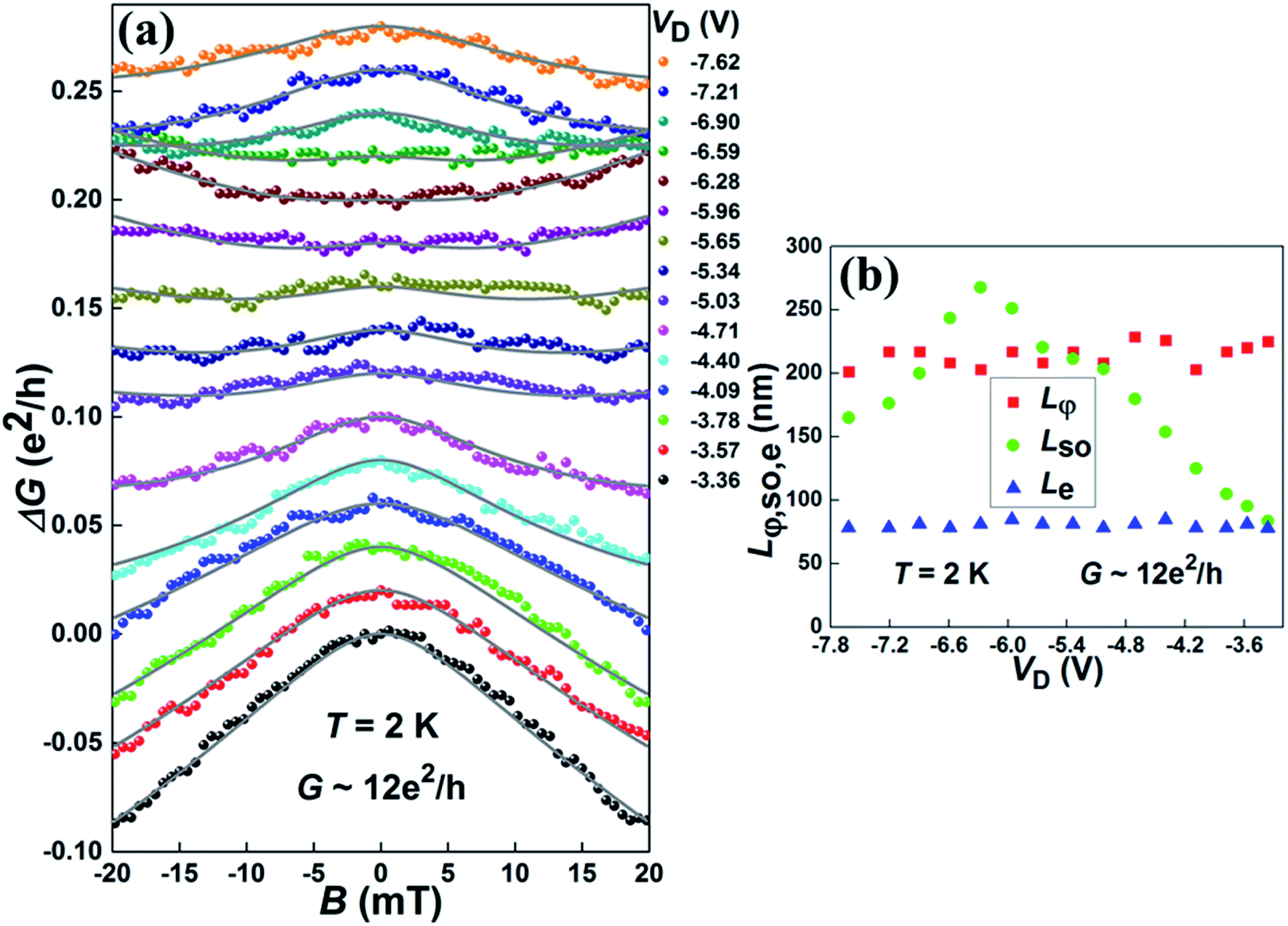 | ||
| Fig. 3 (a) Low-field magnetoconductance ΔG measured for Device 1 at T = 2 K and at dual-gate voltages VD taken along the contour of G ∼ 12e2/h. Here, ΔG = G(B) − G(B = 0), VD = VBG − VTG, and the applied magnetic field B is perpendicular to the InAs nanosheet plane. The bottom black data points display the measured ΔG at VD = −3.36 V and the ΔG data measured at other values of VD are successively vertically offset by 0.02e2/h for clarity. The gray solid lines represent the results of the fits of the measured data to the HLN theory [eqn (1)]. (b) Characteristic transport lengths Lφ, LSO, and Le extracted from the fits in (a) as a function of VD. | ||
To quantitatively analyze the tuning of the SOI in the InAs nanosheet, we fit the measured ΔG data to the HLN formula [eqn (1)]. The solid lines in Fig. 3(a) represent the results of the fits. Fig. 3(b) displays the extracted values of Lφ, LSO, and Le from the fits as a function of VD at a fixed conductance value of G ∼ 12e2/h. It is seen that the extracted Lφ displays a weak dependence on VD and stays at Lφ ∼ 214 nm. This is consistent with the fact that the electron dephasing in the nanosheet is dominantly originated from the electron–electron interaction at low temperatures, which remains approximately unchanged without a change in the carrier density. It is also seen that the extracted Le is also weakly dependent on VD and has a value of Le ∼ 82 nm. This value is consistent with the value of ∼85 nm extracted from the gate transfer characteristic measurements. However, the extracted LSO exhibits a strong dependence on VD. As VD decreases from −3.36 V to −6.28 V, LSO increases from ∼83 nm to ∼268 nm. As VD further decreases, LSO turns to decrease and has a value of ∼165 nm at VD = −7.62 V. A smaller LSO indicates a stronger spin relaxation. Thus, the electrons in the InAs nanosheet of Device 1 exhibit a weak spin relaxation at VD = −6.28 V, but the spin relaxation gets stronger when VD moves away from the value of VD = −6.28 V. Similar low-field magnetoconductance ΔG measurements have also been carried out for Device 1 along the constant conductance contours of G ∼ 7e2/h and G ∼ 4e2/h at T = 2 K (see Section IV and Fig. S4 in the ESI†). These measurements display again the transition from the WAL to the WL and then back to the WAL characteristic with decreasing dual-gate voltage VD along a constant conductance contour (i.e., a constant carrier density). The extracted spin–orbit length LSO at each constant carrier density again appears to be greatly tunable by dual-gate voltage VD and exhibits a peak value at which the strength of the SOI is at a minimum value.
Since, in all the above magnetotransport measurements, the tuning of VD is made along a constant conductance contour and thus approximately at a constant carrier density in the InAs nanosheet, a change in LSO with decreasing VD is most probably due to a change in the perpendicular electric field and thus tuning of the Rashba SOI in the InAs nanosheet. To support this, we have simulated the energy band diagrams of the HfO2/InAs/SiO2 sandwiched layer structure in Device 1 at different dual-gate voltages and carrier densities based on Poisson's equation with the input material parameters of HfO2, InAs, and SiO2 as listed in Table S2 of the ESI† (see Section III in the ESI† for further details). Fig. 4(a) and (b) show, respectively, the simulated bottom conduction-band energies EC and the extracted out-of-plane electric field distributions in the InAs nanosheet with a carrier density of n ∼ 1.34 × 1012 cm−2 (corresponding to the nanosheet conductance G ∼ 12e2/h) for a few experimentally applied dual-gate voltages VD. It is seen that at VD = −3.36 V, the simulated EC is strongly downward tilted, leading to the presence of strong, positive, out-of-plane electric fields and thus the presence of strong Rashba SOI in the InAs nanosheet. As VD decreases, the simulated EC becomes less downward tilted and thus the out-of-plane field strength is reduced, leading to a decrease in the Rashba SOI strength. At the point when VD = −6.28 V, the simulation gives a flat EC profile and thus zero electric field inside the InAs nanosheet. As a result, no Rashba SOI should be present in the InAs nanosheet. When continuously decreasing VD to VD = −7.62 V, the simulated EC becomes upward tilted, leading to the presence of negative, out-of-plane electric fields in the InAs nanosheet and thus a reappearance of the Rashba SOI. Nevertheless, at VD = −7.62 V, the field strength in the nanosheet is in general less than that at VD = −3.36 V. Thus, the Rashba SOI at VD = −7.62 V is weaker when compared that at VD = −3.36 V. The evolution of the Rashba SOI in the InAs nanosheet with decreasing VD, inferred above from the simulation, is consistent with our observation shown in Fig. 3. Thus, tuning spin–orbit length LSO in the InAs nanosheet from a short value to a long value and then back to a short value originates from tuning the Rashba SOI by the dual gate. Note that in the experiment, at VD = −6.28 V, LSO does not go to infinity. This is because a weak, but finite, dual-gate voltage independent SOI term is present in the InAs nanosheet. This term is dominantly of the Dresselhaus type as a result of breaking of bulk inversion symmetry in the InAs compound crystal.
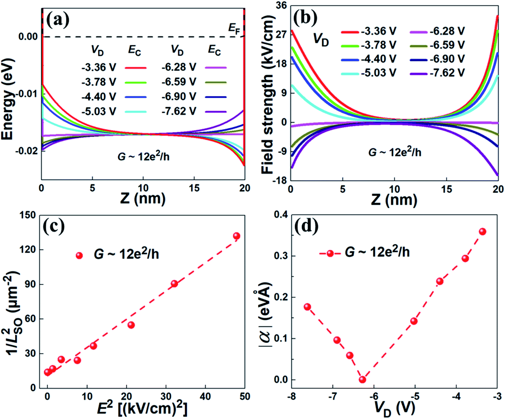 | ||
Fig. 4 (a) Simulated conduction band minimums EC in the InAs nanosheet with a fixed value of n ∼ 1.34 × 1012 cm−2 (corresponding to G ∼ 12e2/h) for Device 1 at different VD values. (b) Corresponding effective out-of-plane electric fields in the InAs nanosheet. (c) Extracted  versus evaluated E2 in the InAs nanosheet. Here, E represents the average out-of-plane electric field strength in the nanosheet and the dashed line represents a linear fit to the data points. (d) Estimated values of the Rashba spin–orbit coupling constant |α| in the InAs nanosheet of Device 1 at a few experimentally applied values of VD. versus evaluated E2 in the InAs nanosheet. Here, E represents the average out-of-plane electric field strength in the nanosheet and the dashed line represents a linear fit to the data points. (d) Estimated values of the Rashba spin–orbit coupling constant |α| in the InAs nanosheet of Device 1 at a few experimentally applied values of VD. | ||
In many cases, it could be convenient to characterize the Rashba SOI strength using the Rashba spin–orbit coupling constant α defined as α = rRE, where E is the average strength of the out-of-plane electric fields E in the InAs nanosheet and rR is a material-specific, Fermi-level dependent prefactor found in the Rashba SOI Hamiltonian HR = rRσ·k × E.23 Since the Rashba spin–orbit precession length is given by  (where m* is the electron effective mass), one can write, to a good approximation, the measured spin–orbit length LSO as
 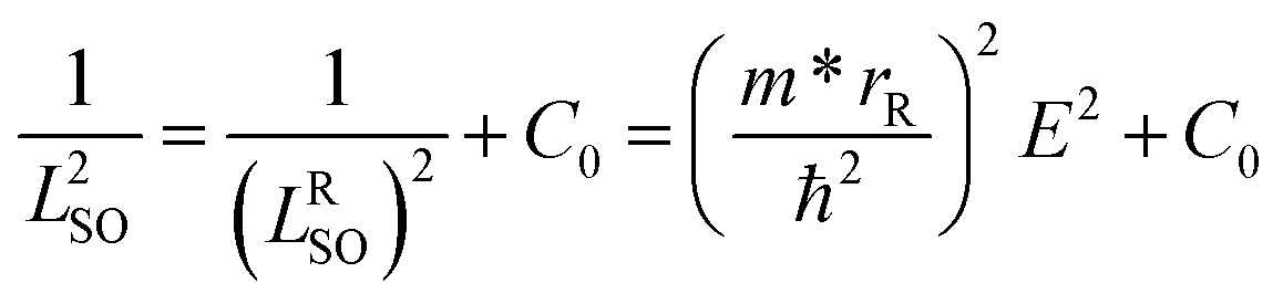 , where C0 takes into account all the electric field-independent contributions to the spin precession in the InAs nanosheet.12 To estimate the Rashba coupling constant α in the InAs nanosheet, we evaluate the average out-of-plane electric field strengths E at different VD values from the simulated results shown in Fig. 4(b) and plot the extracted
  as a function of E2 as shown in Fig. 4(c) (data points). The dashed line in Fig. 4(c) represents a linear fit to the data points, whose slope gives a value of rR = 51.93 e nm2. Fig. 4(d) shows the extracted values of |α| at the experimentally applied values of VD. It is seen that |α| can be tuned from zero to a value of ∼0.36 eV Å for the InAs nanosheet in Device 1 at a conductance of G ∼ 12e2/h (with the corresponding carrier density of n ∼ 1.34 × 1012 cm−2 in the nanosheet). Note that |α| is plotted and shown in Fig. 4(d) and in fact the Rashba coupling constant α in the InAs nanosheet of Device 1 can be tuned from a large negative value to a large positive value. A value of C0 ∼ 11 μm−2 could also be extracted from the fit shown in Fig. 4(c). If we assume that the remaining field-independent contribution to the spin precession is dominantly from the Dresselhaus SOI in the InAs nanosheet, the Dresselhaus spin–orbit precession length can then be extracted as LDSO ∼ 0.30 μm at a nanosheet conductance of G ∼ 12e2/h. Similar analyses have also been carried out for Device 1 at the conductance values of G ∼ 7e2/h and G ∼ 4e2/h, and the same large tunability in the Rashba coupling constant α has been obtained (see Section V and Fig. S5 in the ESI†). In comparison, we note that the tunable Rashba coupling constants of α ∼ 0.01–0.1 eV Å were observed in the InGaAs quantum well and InAs quantum well structures.32–35
Finally, we discuss the influence of temperature on the quantum transport characteristics of the InAs nanosheet device (Device 1). Fig. 5(a) shows the low-field magnetoconductance ΔG measured for Device 1 at VBG = −6 V and VTG = −0.6 V at temperatures T = 2 to 20 K. At T = 2 K, the measured ΔG displays clearly a peak-like structure near zero magnetic field, indicating that the electron transport in the nanosheet exhibits dominantly the WAL characteristic. As T increases from 2 to 20 K, the WAL characteristic is gradually suppressed. Again, the measured ΔG data at different temperatures are fitted to the HLN formula [eqn (1)]. The solid lines in Fig. 5(a) represent the fitting results. Fig. 5(b) displays the extracted values of Lφ, LSO, and Le as a function of T from the fits. It is generally seen that both LSO and Le show a weak temperature dependence. However, Lφ is strongly dependent on temperature – it decreases from ∼235 to ∼112 nm with increasing T from 2 to 20 K. The extracted Lφ data at different temperatures can be fitted by using the power law of Lφ ∼ T−0.37 [see the solid line in Fig. 5(b)]. This Lφ ∼ T−0.37 dependence suggests that the dephasing of electrons in the InAs nanosheet is dominantly caused by electron–electron interactions with small energy transfers (the Nyquist scattering mechanism).36 Note that the width of the InAs nanosheet conduction channel in the device is only slightly larger than the extracted phase coherence length (W ∼ 410 nm vs. Lφ ∼ 120–230 nm), and the observed Lφ ∼ T−0.37 falls in a result lying between the one-dimensional (T−1/3) and 2D (T−1/2) regime.37
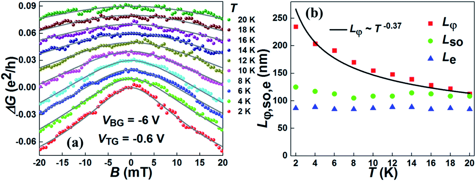 | ||
| Fig. 5 (a) Low-field magnetoconductance ΔG measured for Device 1 at VBG = −6 V and VTG = −0.6 V and at different temperatures T. The bottom red data points display the measured ΔG data at T = 2 K and the ΔG data measured at other temperatures are successively vertically offset by 0.01e2/h for clarity. The gray solid lines represent the results of the fits of the measured ΔG data to the HLN theory [eqn (1)]. (b) Characteristic transport lengths Lφ, LSO, and Le extracted from the fits in (a) as a function of T. The black solid line is a power-law fit of the extracted values of Lφ, showing Lφ ∼ T−0.37. | ||
In summary, a dual-gate field-effect device has been made from an epitaxially grown free-standing InAs nanosheet and studied by transport measurements at low temperatures. It is shown that both the carrier density in the InAs nanosheet and the potential difference across the nanosheet can be tuned independently with the use of a dual gate. The magnetoconductance measurements show that the electron transport in the nanosheet can be tuned from the WAL to the WL and then back to the WAL characteristic by sweeping the dual-gate voltage along a constant nanosheet channel conductance contour. Thus, efficient tuning of the Rahsba SOI in the InAs nanosheet can be achieved at a constant carrier density. The extracted spin-obit length at a constant carrier density is found to exhibit a peak value at which the Rashba SOI is suppressed and the spin relaxation by the Dresselhaus SOI can be revealed. Magnetotransport measurements have also been carried out for a dual-gate device made from another InAs nanosheet and similar results are found (see Section VI in the ESI†). We have also performed the energy band diagram simulations for the layer structure of the dual-gate InAs nanosheet device under experimental conditions and the obtained results support our experimental observations.
Author contributions
H. Q. Xu conceived and supervised the project. F. Fan fabricated the devices, performed the transport measurements and carried out the simulations for energy band diagrams with support from Y. Chen. D. Pan and J. Zhao grew the materials and analyzed the material crystal structures. F. Fan and H. Q. Xu analyzed the transport measurement data and the simulation results. F. Fan and H. Q. Xu wrote the manuscript with contributions from all the authors.Conflicts of interest
There are no conflicts of interests to declare.Acknowledgements
This work was supported by the Ministry of Science and Technology of China through the National Key Research and Development Program of China (Grant Nos. 2017YFA0303304 and 2016YFA0300601), the National Natural Science Foundation of China (Grant Nos. 92165208, 92065106, 61974138, 11874071, 91221202, and 91421303), and the Beijing Academy of Quantum Information Sciences (Grant No. Y18G22). D. P. also acknowledges support from the Youth Innovation Promotion Association, Chinese Academy of Sciences (2017156).References
- C. Thomas, A. T. Hatke, A. Tuaz, R. Kallaher, T. Wu, T. Wang, R. E. Diaz, G. C. Gardner, M. A. Capano and M. J. Manfra, Phys. Rev. Mater., 2018, 2, 104602 CrossRef CAS.
- Ch. A. Lehner, T. Tschirky, T. Ihn, W. Dietsche, J. Keller, S. Fält and W. Wegscheider, Phys. Rev. Mater., 2018, 2, 054601 CrossRef CAS.
- J. Miao, W. Hu, N. Guo, Z. Lu, X. Zou, L. Liao, S. Shi, P. Chen, Z. Fan, J. C. Ho, T. Li, X. S. Chen and W. Lu, ACS Nano, 2014, 8, 3628 CrossRef CAS PubMed.
- H. Fang, W. Hu, P. Wang, N. Guo, W. Luo, D. Zheng, F. Gong, M. Luo, H. Tian, X. Zhang, C. Luo, X. Wu, P. Chen, L. Liao, A. Pan, X. Chen and W. Lu, Nano Lett., 2016, 16, 6416 CrossRef CAS PubMed.
- I. Žutić, J. Fabian and S. D. Sarma, Rev. Mod. Phys., 2004, 76, 323 CrossRef.
- W. Y. Choi, H. Kim, J. Chang, S. H. Han, H. C. Koo and M. Johnson, Nat. Nanotechnol., 2015, 10, 666 CrossRef CAS PubMed.
- Z. Yang, B. Heischmidt, S. Gazibegovic, G. Badawy, D. Car, P. A. Crowell, E. P. A. M. Bakkers and V. S. Pribiag, Nano Lett., 2020, 20, 3232 CrossRef CAS PubMed.
- S. Heedt, W. Prost, J. Schubert, D. Grützmacher and Th. Schäpers, Nano Lett., 2016, 16, 3116 CrossRef CAS PubMed.
- F. Fan, Y. Chen, D. Pan, J. Zhao and H. Q. Xu, Appl. Phys. Lett., 2020, 117, 132101 CrossRef CAS.
- C. Mittag, J. V. Koski, M. Karalic, C. Thomas, A. Tuaz, A. T. Hatke, G. C. Gardner, M. J. Manfra, J. Danon, T. Ihn and K. Ensslin, Phys. Rev. X, 2021, 2, 010321 Search PubMed.
- I. van Weperen, S. R. Plissard, E. P. A. M. Bakkers, S. M. Frolov and L. P. Kouwenhoven, Nano Lett., 2013, 13, 387 CrossRef CAS PubMed.
- Y. Chen, S. Huang, D. Pan, J. Xue, L. Zhang, J. Zhao and H. Q. Xu, npj 2D Mater. Appl., 2021, 5, 3 CrossRef CAS.
- I. Kulesh, C. T. Ke, C. Thomas, S. Karwal, C. M. Moehle, S. Metti, R. Kallaher, G. C. Gardner, M. J. Manfra and S. Goswami, Phys. Rev. Appl., 2020, 13, 041003 CrossRef CAS.
- H. C. Koo, J. H. Kwon, J. Eom, J. Chang, S. H. Han and M. Johnson, Science, 2009, 325, 1515 CrossRef CAS PubMed.
- W. Y. Choi, H. Kim, J. Chang, S. H. Han, A. Abbout, H. B. M. Saidaoui, A. Manchon, K. Lee and H. C. Koo, Nano Lett., 2018, 18, 7998 CrossRef CAS PubMed.
- S. Nadj-Perge, S. M. Frolov, E. P. A. M. Bakkers and L. P. Kouwenhoven, Nature, 2010, 468, 1084 CrossRef CAS PubMed.
- S. Nadj-Perge, V. S. Pribiag, J. W. G. van den Berg, K. Zuo, S. R. Plissard, E. P. A. M. Bakkers, S. M. Frolov and L. P. Kouwenhoven, Phys. Rev. Lett., 2012, 108, 166801 CrossRef CAS PubMed.
- S. Vaitiekėnas, G. W. Winkler, B. van Heck, T. Karzig, M. T. Deng, K. Flensberg, L. I. Glazman, C. Nayak, P. Krogstrup, R. M. Lutchyn and C. M. Marcus, Science, 2020, 367, eaav3392 CrossRef PubMed.
- A. Fornieri, A. M. Whiticar, F. Setiawan, E. Portolés, A. C. C. Drachmann, A. Keselman, S. Gronin, C. Thomas, T. Wang, R. Kallaher, G. C. Gardner, E. Berg, M. J. Manfra, A. Stern, C. M. Marcus and F. Nichele, Nature, 2019, 569, 89 CrossRef CAS PubMed.
- M. T. Deng, C. L. Yu, G. Y. Huang, M. Larsson, P. Caroff and H. Q. Xu, Nano Lett., 2012, 12, 6414 CrossRef CAS PubMed.
- V. Mourik, K. Zuo, S. M. Frolov, S. R. Plissard, E. P. A. M. Bakkers and L. P. Kouwenhoven, Science, 2012, 336, 1003 CrossRef CAS PubMed.
- G. Dresselhaus, Phys. Rev., 1955, 100, 580 CrossRef CAS.
- Y. A. Bychkov and E. I. Rashba, J. Phys. C: Solid State Phys., 1984, 17, 6039 CrossRef.
- S. Datta and B. Das, Appl. Phys. Lett., 1990, 56, 665 CrossRef CAS.
- E. I. Rashba and Al. L. Efros, Appl. Phys. Lett., 2003, 83, 5295 CrossRef CAS.
- E. I. Rashba and Al. L. Efros, Phys. Rev. Lett., 2003, 91, 126405 CrossRef CAS PubMed.
- J. W. G. van den Berg, S. Nadj-Perge, V. S. Pribiag, S. R. Plissard, E. P. A. M. Bakkers, S. M. Frolov and L. P. Kouwenhoven, Phys. Rev. Lett., 2013, 110, 066806 CrossRef CAS PubMed.
- D. Pan, J. Wang, W. Zhang, L. Zhu, X. Su, F. Fan, Y. Fu, S. Huang, D. Wei, L. Zhang, M. Sui, A. Yartsev, H. Q. Xu and J. Zhao, Nano Lett., 2019, 19, 1632 CrossRef CAS PubMed.
- S. Hikami, A. I. Larkin and Y. Nagaoka, Prog. Theor. Phys., 1980, 63, 707 CrossRef.
- G. Bergmann, Phys. Rev. Lett., 1982, 48, 1046 CrossRef.
- G. Bergmann, Phys. Rev. B, 1983, 28, 2914 CrossRef CAS.
- J. Nitta, T. Akazaki, H. Takayanagi and T. Enoki, Phys. Rev. Lett., 1997, 78, 1335 CrossRef CAS.
- T. Koga, J. Nitta, T. Akazaki and H. Takayanagi, Phys. Rev. Lett., 2002, 89, 046801 CrossRef PubMed.
- B. Shojaei, P. J. J. O'Malley, J. Shabani, P. Roushan, B. D. Schultz, R. M. Lutchyn, C. Nayak, J. M. Martinis and C. J. Palmstrøm, Phys. Rev. B, 2016, 93, 075302 CrossRef.
- A. T. Hatke, T. Wang, C. Thomas, G. C. Gardner and M. J. Manfra, Appl. Phys. Lett., 2017, 111, 142106 CrossRef.
- B. L. Altshuler, A. G. Aronov and D. E. Khmelnitsky, J. Phys. C: Solid State Phys., 1982, 15, 7367 CrossRef CAS.
- T. Ando, A. B. Fowler and F. Stern, Rev. Mod. Phys., 1982, 54, 437 CrossRef CAS.
Footnote |
| † Electronic supplementary information (ESI) available. See https://doi.org/10.1039/d2na00143h |
| This journal is © The Royal Society of Chemistry 2022 |