DOI:
10.1039/D1NA00891A
(Paper)
Nanoscale Adv., 2022,
4, 1608-1616
Tailoring TiO2/Al2O3 heterolayers as optical filters for the visible region†
Received
26th December 2021
, Accepted 7th February 2022
First published on 18th February 2022
Abstract
Optical filters operating in the visible region of the spectrum are highly desired for applications ranging from optical communication and sensing to fluorescence microscopy and skin therapy. However, complex fabrication procedures and/or inferior performance, limit the practical applications of previously reported thin-film-based optical filters. Herein, we describe the structual design concepts and facile fabrication of vertically stacked heterolayers of TiO2/Al2O3 to obtain a bandpass filter and a longwave pass edge filter operating in the spectral range 410–600 nm and 400–597 nm, respectively. The optical filters are designed according to MacLeod simulation and fabricated via magnetron sputtering, depositing alternative stacks of low (Al2O3) and high (TiO2) refractive index materials with different thicknesses, as confirmed by spectroscopic ellipsometry. Owing to a reasonable matching between the design and the fabrication, our developed TiO2/Al2O3 heterolayer optical filters exhibited 54.60% transmission for 7-layer longwave pass edge filter and 15% reflectance for 14-layer bandpass filter of a selective set of wavelengths (400–800 nm).
Introduction
Optical and optoelectronic devices1 are considered to be central to epidermal sensing, phototherapy,2 and laser surgery.3 During the last decade, researchers have devoted their efforts to developing materials for optical filters (OFs) operating primarily in the IR region. These efforts are well-supported by computer-aided simulations4 for designing and optimizing OFs with meticulous precision. However, the key parameter deciding the overall performance of the OFs remains pivotal to the choice of materials for the thin film fabrication process. To this end, an ideal material system should have the traits of being highly transparent and non-magnetic. Furthermore, in order to minimize scattering, the material should be homogeneous and isotropic,5 having low sheet resistance.6 Recently, heterolayer-based thin films7 with an optimized combination of interface reflectance losses and refractive indices have emerged as an innovative platform to design and control the spectral wavelength of optical signals for applications including reflecting mirror coatings,8 optical storage devices,9 optical reflectors,10 antireflection coating, OFs,11 and solar cells.12 In OFs, low refractive index (nL) materials and high refractive index (nH) materials are precisely tuned to control the intensity and wavelength range of light.13 There have been reports on the preparation of such heterolayer OFs,14 such as a-Si:H/SiO2 by RF magnetron sputtering,15 TiO2/SiO2 by helicon plasma sputtering,14,16 Er2O3/TiO2 by magnetron sputtering,17 and SrTiO3/ZnTiO3 by spin coating.18
Optical filters based on TiO2/Al2O3 heterolayers, were extensively studied. S. Zaitsu et al. reported TiO2/Al2O3 sublayers fabricated by atomic layer deposition19 by controlling the refractive index, Saraf et al. reported TiO2/Al2O3 multilayer by electron beam evaporation at the wavelength of 650 nm,20 Liu et al. reported TiO2/Al2O3 single layer by electron beam evaporation at 450 nm wavelength,21 Szeghalmi et al. reported TiO2/Al2O3 multilayer by atomic layer deposition at wavelength 400–550 nm,22 Li et al. reported the TiO2/Al2O3 notch filter by atomic layer deposition at 510–590 nm wavelength,23 and Han et al. reported TiO2/Al2O3 multilayers by plasma enhanced atomic layer deposition at different powers in the range of 100–500 W.24 Nevertheless, these fabrication procedures for heterolayers are rather complex but wth inferior performance in the visible region of the spectrum; thus, facile RF magnetron sputtering is adopted to deposite high-quality thin films for optimal results in the visible region. Indeed, TiO2 and SiO2 with high and low refractive indices have been used as high and low refractive films, respectively, to fabricate highly reflective multilayer structures. In this study, we used Al2O3 film instead of SiO2 film to design the multilayer reflective coating because the refractive index of the Al2O3 film has a stable value of 1.74, whereas the refractive index of SiO2 film decreases from 1.47 to 1.45 as the wavelength of optical light increases from 400 to 1000 nm. Hence, we used the RF magnetron sputtering method to deposit Al2O3 and TiO2 single-layer films and Al2O3–TiO2 heterolayer films on glass substrates to create reflective coatings.
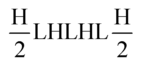
OFs operation in the visible region of the spectrum have been also reported with the use of noble metals such as gold (Au),25 silver (Ag),26 and rare earth elements,27 or with complex fabrication processes.21,28 Therefore, earth-abundant low-cost materials (TiO2 and Al2O3) and facile fabrication process are employed. RF magnetron sputtering deposition technique provides precise control of thickness and nanostructure. OFs can be tailored according to the required transmission and reflectance at selected spectral wavelengths by manipulating the design, thicknesses, and the choice of material of the thin-film heterolayers. With lower refractive index ratio, more layers are required to achieve good and precise results of transmission and reflectance, thus endowing thin heterolayered structures with reflective properties at some wavelengths and transmitting at others. In the present work, OFs were designed with quarter-wave (QW)29 stacks of alternating high and low refractive index TiO2–Al2O3 thin film heterolayers deposited on an optical barium borosilicate glass (7059) substrate using RF magnetron sputtering.30 We first simulate the design of the heterolayers HHLHHLHHLHHLHH as a bandpass filter,  as a longwave pass edge filter, followed by depositing heterolayers by RF magnetron sputtering. The custom design renders the as-fabricated heterolayers assembly to transmit at a precise set of wavelengths (400–800 nm), while reflecting the others.31,32 Achieving transmission of 54.60% and reflectance of 15%, we believe that our designed bandpass and longwave pass edge filters are ideally suited for applications in satellites, loud speakers,33 audio amplifiers,34 data conversion,35 and heart rate metric extractor.36 Out of many material combinations, the titania–alumina combination is the widely used multilayer stack for AR and reflective mirror applications. Commercially used wireless transmitters show sharp edges.
Designing of optical filters (OFs)
Bandpass filter
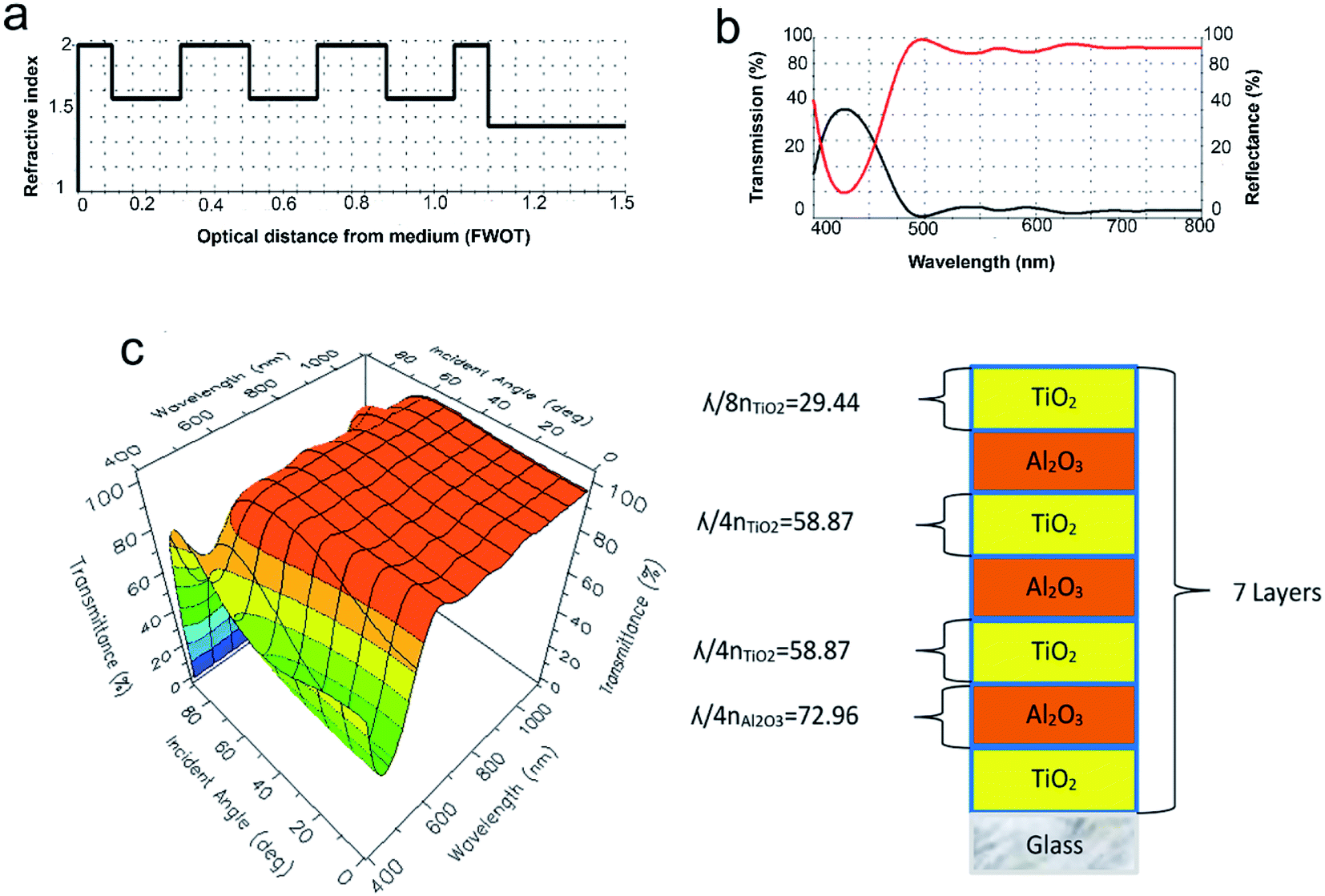
The heterolayers stack of alternate TiO2/Al2O3 thin films was simulated in Essential MacLeod (Fig. S1†) thin film design software (see Note S1†). The design for the bandpass filter was air [2TiO2Al2O3]4 2TiO2 glass. As a function of thickness in the z-direction, the refractive index profile of the heterolayers stack is represented in Fig. 1(a). The simulation result of air [2TiO2Al2O3]4 2TiO2 glass heterolayer stack was for 0° incidence at the reference wavelength of 510 nm. TiO2 layers with a refractive index of 2.16 served as the high index layer (nH) and Al2O3 layers with a refractive index of 1.74 behaved as the low index layer (nL) at a specific wavelength 510 nm; those mentioned in the Introduction are the refractive indices of amorphous materials, which are not at a specific wavelength. The thickness of each layer in the 14-layer bandpass filter of TiO2 and Al2O3 was the quarter-wave stack design (see Table 1). In this design, double-layer TiO2 and single-layer Al2O3 were alternately used in such a way that the start and end layer of the design were double-layer TiO2. Each TiO2 layer has a thickness of ¼ of the quarter-wave, which is 14.72 nm, and each Al2O3 has a thickness of ½ of the quarter-wave, which is 36.48 nm. The total thickness of the designed heterolayer was 293.12 nm. The transmission and reflectance spectra of the simulation of the 14-layer bandpass filter are shown in Fig. 1(b). Reflectance increased as the wavelength increased from 410 nm and maximum reflection was 19.57% at 480 nm; here, the transmission was minimum (80.06%). After 480 nm, reflectance began decreasing and obtained a minimum value of 4% at 600 nm; here, the transmission was maximum (96%). After 600 nm wavelength, the reflectance began to increase and transmission began to decrease, the resonance wavelength of the [2TiO2Al2O3]4 2TiO2 film was 510 nm and each TiO2 layer in the stack had a thickness of a quarter of the quarter-wavelength 1/4(λ/4n), while Al2O3 had a thickness of half the quarter-wavelength 1/2(λ/4n). Here, n represents the refractive index of TiO2 and Al2O3 at the designed wavelength. The total thickness of this design was 293.12 nm. To check the performance of this work, more designs of optical filters were prepared in different wavelength ranges, e.g., 14-layer bandpass filter in the infrared region of the spectrum (see Table S1†), transmission spectra, and 3D view (Fig. S2†), and the physical design (see Table S2†), transmission spectra, and 3D view of the 17 layers are given in Fig. S3(a) and (b),† while the 20 layers design (see Table S3†), transmission spectra, and 3D view are given in Fig. S3(c) and (d);† all the bandpass filters were in the visible region but the results were not very good.
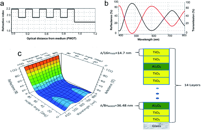 |
| | Fig. 1 (a) Theoretical calculation (simulated physical design) of the changes in the refractive index versus optical distance from the medium (FWOT) thickness with reference wavelength of 510 nm at 0° angle of incidence. (b) Transmission (%) and reflectance (%) spectra versus wavelength (nm) in the visible region of the spectrum; black color is reflectance (%) and red color is transmission (%). (c) Three-dimensional (3D) shape of the reflectance (%) spectra versus wavelength (nm) with the angle of incidence (deg) and physical design of alternative quarter-wave stack 14 layer design [2TiO2Al2O3]4 2TiO2 on glass substrate and air, which was the medium bandpass filter. | |
Table 1 Simulated design of bandpass filter with reference wavelength 510 nm
| Materials |
Thickness (nm) |
| TiO2 |
14.72 |
| TiO2 |
14.72 |
| Al2O3 |
36.48 |
| TiO2 |
14.72 |
| TiO2 |
14.72 |
| Al2O3 |
36.48 |
| TiO2 |
14.72 |
| TiO2 |
14.72 |
| Al2O3 |
36.48 |
| TiO2 |
14.72 |
| TiO2 |
14.72 |
| Al2O3 |
36.48 |
| TiO2 |
14.72 |
| TiO2 |
14.72 |
Longwave pass edge filter
The heterolayers stack of alternate TiO2/Al2O3 layers was simulated in Essential MacLeod thin film design software. The design for the longwave pass edge filter was air  Al2O3TiO2Al2O3TiO2 Al2O3
 glass. The physical thicknesses of TiO2 were taken as 29.44 nm for the first and last layers, and 58.87 nm for the alternate layers, while Al2O3 had a thickness of 72.96 nm for each layer at the central wavelength of 510 nm. The refractive index values were 2.16 and 1.74 for TiO2 and Al2O3, respectively, as a function of thickness in the z-direction; the refractive index profile of the heterolayers stack is represented in Fig. 2(a). The thickness of each layer for the longwave pass edge filter design is shown in Table 2. The design consists of seven alternative layers of TiO2 and Al2O3, which have a quarter-wave thickness of 58.87 nm and 72.96 nm, respectively. The start and end layer of the design was TiO2, which has a thickness of half the quarter-wavelength 29.44 nm. The total thickness of this design was 395.5 nm. The simulation result of air
  Al2O3TiO2Al2O3TiO2 Al2O3
 glass heterolayers stack was for 0° incidence at the reference wavelength of 510 nm. TiO2 layers with a refractive index of 2.16 acted as the high index layer (nH) and Al2O3 layers with a refractive index of 1.74 behaved as the low index layer (nL). The thickness of each layer was a quarter-wave stack for this design. Wherever reflectance was minimum, transmission would be maximum. At 400 nm, the transmission value was 75.86%. After 400 nm, the transmission value began to decrease to 40.26% at 461 nm. After 475 nm, there was an abrupt increase in the transmission at 597 nm, where the transmission had the maximum value of 100% and the reflectance was 0%. To check the performance of longwave pass edge filter in visible region more design of optical filter in different wavelength range and also different heterolayers 7-layer longwave pass edge filter in visible region but reference wavelength 563 nm Fig. S4(a)† physical design (see Table S4†), infra-red region reference wavelength 810 nm Fig. S4(c)† design (see Table S5†), and physical design (see Table S6†) transmission spectra ultraviolet Fig. S4(d)† region of spectrum with reference wavelength 400 nm. Seven layer longwave wave pass edge filter but material was TiO2 and ZrO2 reference wavelength 563 nm Fig. S4(b)† but the result was too good in 510 nm used as reference wavelength.
 |
| | Fig. 2 (a) Theoretical calculation (simulated physical design) of the changes in the refractive index versus optical distance from the medium (FWOT) thickness with the reference wavelength of 510 nm at 0° angle of incidence. (b) Transmission (%) and reflectance (%) spectra versus wavelength (nm) in the visible region of the spectrum; black color is reflectance (%) and red color is transmission (%). (c) Three-dimensional (3D) shape of the transmission (%) spectra versus wavelength (nm) with the angle of incidence (deg) and physical design of the alternative quarter-wave stack 7-layers design  Al2O3TiO2Al2O3TiO2 Al2O3 Al2O3TiO2Al2O3TiO2 Al2O3 on glass substrate and air, which was the medium longwave pass edge filter. on glass substrate and air, which was the medium longwave pass edge filter. | |
Table 2 Simulated design of longwave pass edge filter with reference wavelength 510 nm
| Materials |
Thickness (nm) |
| TiO2 |
29.44 |
| Al2O3 |
72.96 |
| TiO2 |
58.87 |
| Al2O3 |
72.96 |
| TiO2 |
58.87 |
| Al2O3 |
72.96 |
| TiO2 |
29.44 |
Experimental section
Single-layer TiO2 and Al2O3 thin films were deposited on glass substrate by RF magnetron sputtering (see Table 3). During deposition, argon flow of the ion source was kept at 50 sccm with a pressure of 1.5 Pascal and RF power was kept at 50 W. The deposition parameters remained constant in all the depositions.
Table 3 Working parameters for RF magnetron sputtering deposition of the thin films
| Power |
50 W to 100 W |
| Time |
30 min to 60 min |
| Target |
Al2O3, TiO2 |
| Gas flow |
50 sccm |
| Pressure |
1.5 Pascal |
| Gas |
Argon |
Fabrication of thin films
RF magnetron sputtering (Fig. S5(a)†) is required for dielectric materials. A generator RF magnetron sputtering system (Model PFG 600 RF) was used for the deposition. Barium borosilicate glass (7059) was used for the deposition of thin films. 7059 glass substrates were precleaned sequentially with detergent washing, ultrasonication with acetone, ultrasonication with IPA, and drying by nitrogen gas flow. To achieve the maximum purification of the thin film, ultrahigh vacuum was required. A rotary pump was used as the backing pump to create rough vacuum in the range of 10−1 torr (13.3 Pascal). With the rough vacuum obtained, the turbo-molecular pump was used to create vacuum in the range of 10−6 torr (1.3 × 10⁻³ Pascal).
Thin film characterization
Spectroscopic ellipsometry (see Note S2†) is an optical technique in which samples are analyzed through modeling to obtain the physical properties. Film thicknesses, transmittance, reflectance, optical absorption, bandgap energy extinction coefficient, and refractive index were calculated in a specific range of wavelength. Typically, isotropic-layered or bulk materials are characterized using the following equation.Here, “ψ” represents the wavelength and “Δ” represents the change in the wavelength.
Spectroscopic ellipsometry characterization (Fig. S5(b)†) depends on individual layer thickness, properties of the light beam (polarization, angle of incidence, and wavelength), material properties, and reflectivity of the spectra. It is an indirect process as the samples' physical parameters are extracted from the recorded spectra. Spectroscopic ellipsometry was measured in terms of Δ and ψ. M-2000, RC 2, and Accu Map-SE map systems (by J. A. Woollam Co.) ellipsometry were used to measure the optical constants and optical spectrum of the TiO2 and Al2O3 thin films. It has wavelength in the range of 290–1790 nm. Transmission and reflectance were measured at 0° and 45°, respectively. Parallel-polarized light was used in the experiment. Probing light was used in the visible range (300–900 nm). Δ represents phase difference between the perpendicular and parallel components of reflected and incident rays. Ψ was the angle whose tangent represents the ratio between the magnitudes of total reflection coefficient (1–2 μm). Ψ and Δ cannot be directly changed into the optical coefficients of the sample.
Results and discussion
Properties of Al2O3 and TiO2 single layer
The values of refractive index (n) and extinction coefficient (k) of Al2O3 and TiO2 are represented in Fig. 3(a) and (b), respectively. The refractive index curves of Al2O3 and TiO2 show a similar pattern with wavelength above 450 nm. For Al2O3, the refractive index decreased with increasing wavelength as its relation was inverse to the wavelength. At 300 nm, the refractive index had a maximum value of 2.145. In the range of 300–480 nm, the value of the refractive index changed gradually, and beyond 500 nm, its value became almost constant. The extinction coefficient exhibited inverse variation with wavelength. At 300 nm, the extinction coefficient had a maximum value of 0.34. In the range of 300–350 nm, the change in the extinction coefficient with wavelength was very small and there was no visible change in the extinction coefficient values with wavelength after 350 nm.37 The change in the relations between the extinction coefficients and refractive indices with the wavelength in the graph were almost the same. For TiO2, the value of refractive index increased as the wavelength changed from 300 to 358 nm. At 358 nm, the refractive index had a maximum value of 2.54. In the range of 360–780 nm, the refractive index decreased as the wavelength increased. Meanwhile, the extinction coefficient monotonously decreased as the wavelength increased and had a maximum value of 0.70 at 300 nm wavelength.38 For bandpass filter (14-layer) and longwave pass edge filter (7-layer), the deposition rate of Al2O3 and TiO2 for one layer was 1.193 nm min−1 and 1.23 nm min−1, respectively, determined by dividing the total thickness of the single layer by the total deposition time at 50 W power. In the range of 280–300 nm, the value of transmission was almost zero. There was an abrupt change in transmission from 300 to 380 nm and the transmission was 49.5% at 380 nm wavelength. There was a gradual increase in the transmission with increasing wavelength from 400 to 600 nm. At 572 nm, transmission had a maximum value of 82.4%. Beyond 572 nm, the transmission value started to decrease very slowly and the value of transmission was almost constant after 600 nm (Fig. S6(a)†). From 300 to 342 nm, the transmission increased abruptly, followed by a gradual increase with wavelength (Fig. S6(b)†). Transmission has a maximum value of 78.2% at 900 nm. To determine the bandgap of Al2O3 and TiO2, we draw a graph between the absorption coefficient and energy for Al2O3 and TiO2, as shown in Fig. 3(c) and (d), respectively. If we get a straight line graph using the α2 value, then the film will have direct bandgap, but if we get a straight line using 1/α, then the thin film has indirect bandgap. However, we can only find the relationship of α2 with energy.
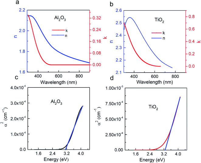 |
| | Fig. 3 (a) Spectroscopic ellipsometry measurement of refractive index (n) and extinction coefficient (k) behavior of sputtered Al2O3 single layer versus wavelength (nm) in the visible region of the spectrum. (b) Refractive index (n) and extinction coefficient (k) behavior of TiO2versus wavelength (nm). (c) Absorption coefficient (α2 (cm−1)) versus optical bandgap energy (eV) for Al2O3 single layer direct bandgap. (d) Absorption coefficient (α2 (cm−1)) versus optical bandgap energy (eV) for TiO2 of single layer direct bandgap. | |
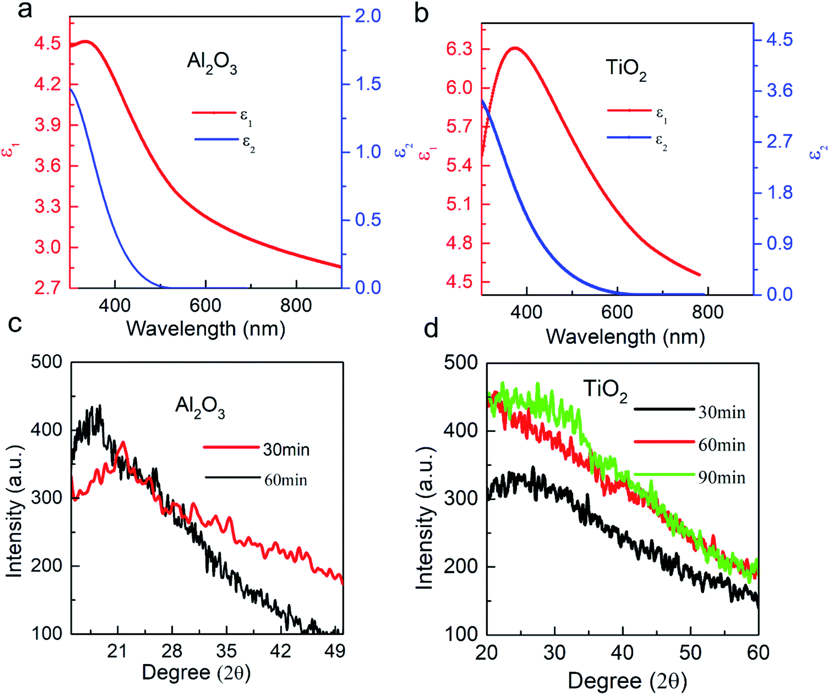
The calculated real and imaginary parts of the dielectric function of our materials are shown in Fig. 4(a) and (b), respectively. The real part gave information about how much light was transmitted and the imaginary part gave information about how much light was absorbed by the material. For Al2O3, its imaginary part of the dielectric function decreased with increasing wavelength. The maximum value of the real part of the dielectric function for Al2O3 was 4.51 at 334 nm. From 340 to 550 nm, the value of the real part changed steeply; beyond this range, it decreased gradually. The imaginary part of the dielectric function changed gradually with wavelength decreasing from 300 to 600 nm. After 600 nm, the value of the imaginary part became constant with increasing wavelength. The XRD patterns of Al2O3 and TiO2 thin films deposited for different times are shown in Fig. 4(c) and (d). The graphical behavior showed that the thin film of Al2O3 and TiO2 was amorphous for all the samples deposited at different times. They were only changed in the intensity with increasing deposition time, and there were no changes in the crystallites of these thin films. Our films are amorphous not crystalline; hence, the XRD patterns show us the clear structure of the material. The relationship of thickness with time was direct, i.e., if the deposition time was increased, the thickness of the thin film was also increased. The thickness of the thin film was obtained by ellipsometry.39
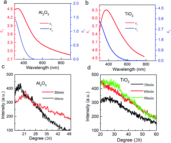 |
| | Fig. 4 (a) Real dielectric (ε1) constant and imaginary dielectric (ε2) constant of the fabricated single layer Al2O3versus wavelength (nm) in the visible region of the spectrum, showing dielectric loss with the increase in the wavelength. (b) Real dielectric (ε1) constant and imaginary dielectric (ε2) constant of the fabricated single layer TiO2versus wavelength (nm). (c) X-ray diffraction patterns of samples of Al2O3 thin films at different deposition times (30 min, 60 min), showing the amorphous behavior of the thin films. (d) X-ray diffraction patterns of samples of TiO2 thin films at different deposition times (30 min, 60 min, and 90 min). | |
Because the films are amorphous, they are good for preparing optical filters. If the films are crystallized, then the bandpass and edge filters do not show transmission curves. Generally, for the same material, the one with a single crystal state is stronger than the amorphous one, which may be due to structural differences that amorphous materials contain, such as dangling bonds or defects, strain, and dislocations, which are more than that in the single crystal states. Thus, in the present study, we have focused on the amorphous property for preparing optical filters. The thickness of the thin films and the fabrication time are proportional to each other in the XRD signals. If there is a variation in the intensity of the XRD peaks for the same material, it can be attributed to the crystallite size variations resulting from many other variables.40
Properties of the heterolayer thin films
Bandpass filter.
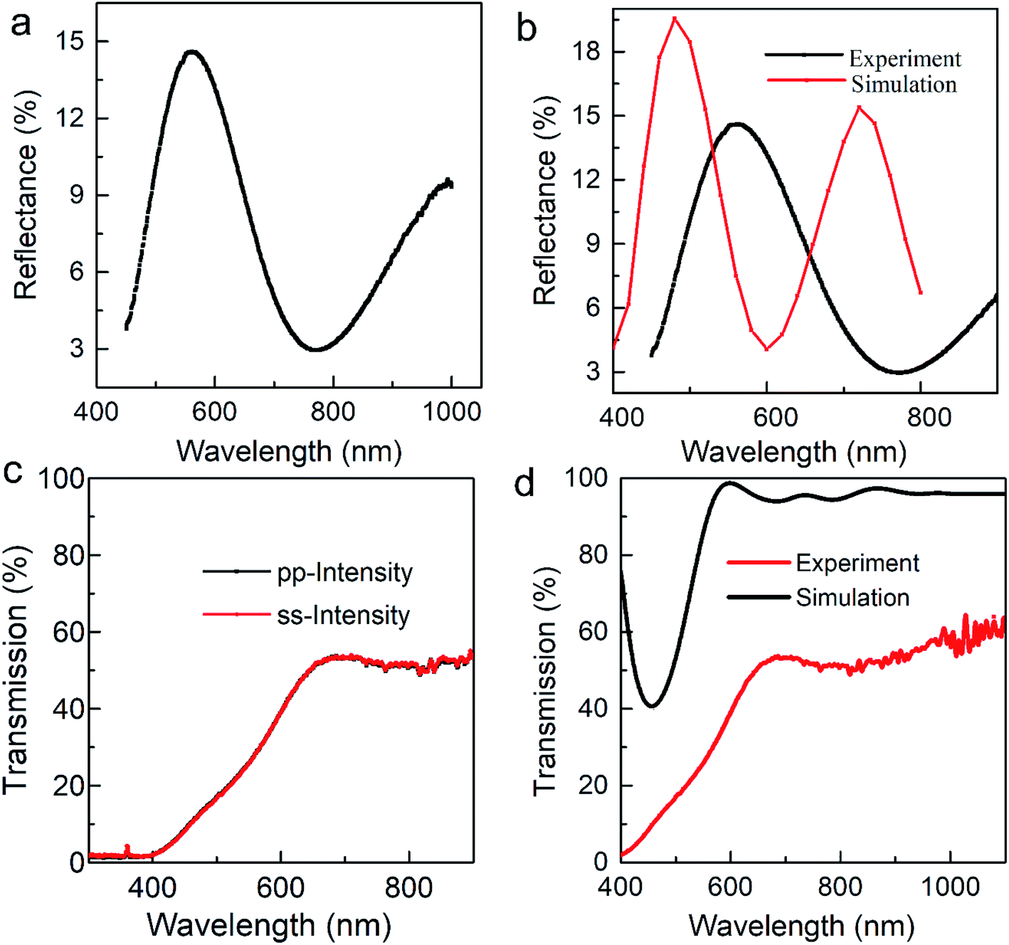
[2TiO2Al2O3]4 2TiO2 films, which act as an optical bandpass filter, were prepared using RF magnetron sputtering. By changing the films' deposition time and power, we can control the thickness of the deposited films. We deposited 14 layers of Al2O3 and TiO2 film on a single substrate and the deposition time for each layer was 30 min. The role of the number of layers in the reflectance (%) spectra is represented in Fig. 5(a); the reflectance (%) of these heterolayers films and thickness are calculated by the M-probe technique. The thickness of these alternated films was 382.2 nm, as measured by the spectroscopic ellipsometry technique and verified by M-probe, while the design thickness was 293.12 nm. There was a difference of 34.48 nm between the thickness of the simulated and the designed stack. This stack had a reflectance of 4% at 450 nm after the wavelength reflectance (%) increased and has a maximum value at 550 nm, where the reflectance was almost 15%. After 550 nm, the reflectance decreased gradually as the wavelength increased. However, the maximum value of reflectance was 19.57% at almost 480 nm wavelength in the simulated design. In design, reflectance (%) was again minimum at 600 nm but the experimental result gave us the minimum value at 770 nm. In Fig. 5(b), the comparison of experiment and simulated results of reflectance (%) showed that with the wavelength at 30 min and 50 W, the reflection was less than that for 60 min and 90 min.41 Thus, we can say that the thin films were transparent. The average transmission value was 75% when the average reflection was 15%. The trend of the reflection graph changed with wavelength and showed small reflection. The reflection of single layer Al2O3 and TiO2 was also determined using spectroscopic ellipsometry (Fig. S6(c) and (d)†).
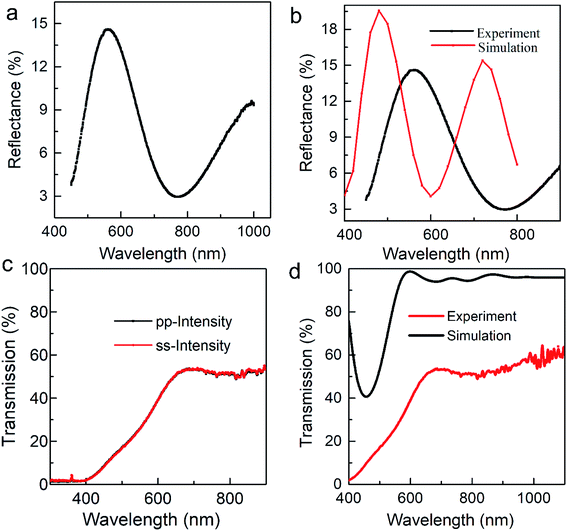 |
| | Fig. 5 (a) Reflectance (%) spectra versus wavelength (nm) of alternatively quarter-wave stacked 14 heterolayers [2TiO2Al2O3]4 2TiO2 on glass substrate bandpass filter. (b) Comparison of the performance of simulated (physical design) and experimental (fabricated) reflectance (%) spectra versus wavelength (nm) in the 400–900 nm range. (c) Transmission (%) spectra versus wavelength (nm) of alternatively quarter-wave stacked 7 heterolayers  Al2O3TiO2Al2O3TiO2Al2O3 Al2O3TiO2Al2O3TiO2Al2O3 on glass substrate longwave pass edge filter at both the intensity values of transmission (%) show the same behavior. (d) Comparison of the performance of simulated (physical design) and experimental (fabricated) transmission (%) spectra versus wavelength (nm) in the 400–1000 nm range. on glass substrate longwave pass edge filter at both the intensity values of transmission (%) show the same behavior. (d) Comparison of the performance of simulated (physical design) and experimental (fabricated) transmission (%) spectra versus wavelength (nm) in the 400–1000 nm range. | |
Longwave pass edge filter.
At 50 W power, we deposited 7 layers of Al2O3 and TiO2 films on a single substrate. The deposition time for the starting and the end layer of TiO2 was 25 min and for other layers, it was 48 min. For Al2O3, the deposition time was 62 min for each layer. The role of the number of layers in the transmission (%) spectra is represented in Fig. 5(c); the transmission (%) of these heterolayer films were calculated by the M-probe technique. The thickness of these alternated films is 408.89 nm, as measured by spectroscopic ellipsometry technique, while average design thickness was 395.49 nm; there was a difference of 13.41 nm. This stack has a transmission of 54.60% at 692.9 nm, beyond which average transmission (%) decreased till 810.74 nm (50.41%). After 810 nm, transmission increased again and attained a maximum value at 1027 nm, where transmission is almost 64.42%. However, in simulation at 400 nm, the transmission value is 75.86%; beyond 400 nm, the transmission value decreased to 40.26% at 461 nm. After 475 nm, there was an abrupt increase in the transmission at 597 nm; the transmission has a maximum value of 100% and reflectance is 0%. We can say that this shift in the wavelength and decrease in the transmission (%) was as a result of the variation of average thickness (thickness of average heterolayer stack and individual layers) due to some human error and technical error. Moreover, average thin layers of TiO2 and Al2O3 deposited by RF magnetron sputtering have no crystalline structure at all, which can be another reason for the shift in the edge and decrease in the transmission. The optical transmittance spectra of the prepared Al2O3 and TiO2 films were measured by ellipsometry (variable angle spectroscopic ellipsometry) and verified by the M-probe technique. Transmission was taken at normal incidence at 0° angle as the films were uniformly (when we measured the thickness by M-probe, there is only a difference of 1–2 nm) deposited across a 6 cm distance. The deposition time was fixed at 30 min and 60 min for Al2O3 and TiO2, respectively. From 280–300 nm, the value of transmission was almost zero. From 300–380 nm, there was an abrupt change in the transmission. At 380 nm, transmission was 49.5%. From 400–600 nm, there was gradual increase in the transmission with the wavelength. At 572 nm, the transmission has a maximum value of 82.4%. Beyond 572 nm, the transmission value starts to decrease very slowly and we can say that after 600 nm, the value of transmission was almost constant. Similarly, for TiO2 the value of transmission increased as the wavelength increased. From 300–342 nm, transmission increased abruptly, followed by the gradual increase in the transmission with wavelength. Transmission has a maximum value of 78.2% at 900 nm. If the number of layers increases, it leads to better filtering property. It should be noted that when refractive index ratio is small, more layers will be needed. Another important result is that when the number of layers increases, the long band pass peak tends toward smaller wavelengths. In Fig. 5(d), a comparison of the experimental and simulated results of transmission (%) with wavelength is given. First, we simulate and then fabricate; due to some defects and other parameters that are involved, the film shows amorphous property when we experimentally fabricate. Therefore, the results do not match but the behavior of the experimental and simulated curves is the same. On the other hand, in simulation, we can easily increase and decrease the thickness of the layers for an ideal result; however, under other experimental factors such as vacuum and film uniformity, we cannot achieve an ideal result. In order to save time, we adopted simulation to guard our experiments. Experimentally, we fabricated the films only with TiO2 and Al2O3 materials but in simulations, we checked other materials' performances as well. The simulation uses ideal parameters, which are quite challenging to achieve experimentally. Therefore, there are discrepancies in the results.
Conclusion
Thin films of Al2O3 and TiO2 prepared by RF magnetron sputtering are laterally uniform. When we measured the thickness (at the center and at the corner of the substrate) by M-probe, there was only a difference of 1–2 nm across 38.1 mm distance from the center. The deposition rate was estimated to be 1.193 nm min−1 and 1.23 nm min−1 for Al2O3 and TiO2, respectively. The transmission values of Al2O3 and TiO2 were 82.4% and 78.2%, respectively. Heterolayer [2TiO2Al2O3]4 2TiO2 bandpass filter and  Al2O3TiO2Al2O3TiO2 Al2O3
 longwave pass edge filter films were deposited alternately on the same substrates with different deposition times (30 min, 60 min) for each layer. The thickness of the bandpass filter by simulation was 293.12 nm and it was 328.2 nm in the experiment. The thickness of the longwave pass edge filter by simulation was 395.5 nm and it was 408.89 nm in the experiment. The maximum transmission of the 7-layer long wave pass edge filter was 99.73% in simulation and 54.60% in the experiment, and the reflectance of the 14-layer bandpass filter was 19% in simulation and 15% in the experiment. The difference in the transmission and reflectance in both the filters may be due to the increase in the thickness of individual or overall stack of layers for the Al2O3 and TiO2 thin films. Investigation of various material composites for manufacturing band pass, band stop, and narrow band pass filter for different applications was done and showed the advantage of the improved optical filters with low losses. The current work can be extended to the fabrication of beam splitters and reflective mirrors.
Conflicts of interest
The authors declare that they have no known competing financial interests or personal relationships that could have appeared to influence the work reported in this paper.
Acknowledgements
The authors acknowledge financial support from the National Natural Science Foundation of China (No. 52073160) and the National Key Research and Development Program of China (No. 2020YFF01014706).
References
- C. Liu, Q. Zhang, D. Wang, G. Zhao, X. Cai, L. Li, H. Ding, K. Zhang, H. Wang and D. J. Kong, Adv. Opt. Mater., 2018, 6, 1800146 CrossRef.
-
V. P. Zharov, Y. A. Menyaev, V. Hamaev, G. Antropov and M. Waner, Optoelectronic microdevices for combined phototherapy, Micro-and Nanotechnology for Biomedical and Environmental Applications, 2000, 3912, p. 11 Search PubMed.
- E. Young, A. Mitchell-Innes and M. J. Jindal, J. Laryngol. Otol., 2015, 129, 627 CrossRef CAS PubMed.
- J. Dorazil, R. Repp, T. Kropfreiter, R. Prüller, K. Říha and F. J. Hlawatsch, IEEE Access, 2020, 8, 222506–222519 Search PubMed.
- X. Li, Z. Zhang and E. J. Pan, Soil Dyn. Earthq. Eng., 2020, 139, 106365 CrossRef.
- G. Schmidl and G. Andrä, Nano-Micro Lett., 2020, 12(1), 1–13 CrossRef PubMed.
- K.-T. Kim, C.-I. Kim and S.-G. J. Lee, Microelectron. Eng., 2003, 66, 662–669 CrossRef CAS.
-
S. D. Bhamare, Determination of Optimal Material Combination for Multilayer Thin Films to Improve Performance Against Surface Crack Propagation, University of Cincinnati, 2009 Search PubMed.
- F. Ghodsi, H. Dashti and J. J. Ahmadi-Shokouh, Opt. Quantum Electron., 2020, 52, 1–16 CrossRef.
- B. Putz, S. Wurster, T. Edwards, B. Völker, G. Milassin, D. Többens, C. Semprimoschnig and M. J. Cordill, Acta Astronaut., 2020, 175, 277–289 CrossRef CAS.
- F.-D. J. Lai, Integr. Ferroelectr., 2020, 210, 64–72 CrossRef CAS.
- S. Jo, J. Y. Woo, J. H. Oh, H. C. Shim, S. Seo, E.-S. Jeon, M. Kim and C.-S. J. Han, ACS Appl. Mater. Interfaces, 2020, 12, 29979–29985 CAS.
- N. Matsumoto, T. Nakagawa, K. Kageyama, N. Wada and Y. J. Sakabe, Jpn. J. Appl. Phys., 2006, 45, 7499 CrossRef CAS.
-
M. Silva, C. Costa, L. Goncalves and J. Correia, TiO2/SiO2 optical filters based on fabry-perot resonators for endoscopy, 2012 Search PubMed.
- H. Yoda, K. Shiraishi, Y. Hiratani and O. Hanaizumi, Appl. Opt., 2004, 43, 3548–3554 CrossRef CAS PubMed.
- X. Wang, H. Masumoto, Y. Someno and T. Hirai, Thin Solid Films, 1999, 338, 105–109 CrossRef.
-
S. Kamikawa, 2008.
- Y. Li, B. Xu, S. Xia and P. J. Shi, J. Adv. Dielectr., 2020, 10, 2050027 CrossRef CAS.
- S.-i. Zaitsu, T. Jitsuno, M. Nakatsuka, T. Yamanaka and S. Motokoshi, Appl. Phys. Lett., 2002, 80, 2442–2444 CrossRef CAS.
-
M. Saraf, M. Kumar, P. Sunita, V. S. P. Kumar, P. K. Rao, N. Kumari, V. Karar and A. L. Sharma, Multi-layer dielectric thin-film optical filters for beam folding applications, 2014, vol. 9654, pp. 90–94 Search PubMed.
- J. Liu, C.-Y. Lin, W.-C. Tzou, N.-K. Hsueh, C.-F. Yang and Y. Chen, Cryst. Growth Des., 2018, 18, 5426–5433 CrossRef CAS.
- A. Szeghalmi, M. Helgert, R. Brunner, F. Heyroth, U. Gösele and M. Knez, Appl. Opt., 2009, 48, 1727–1732 CrossRef CAS PubMed.
- Y. Li, W. Shen, X. Hao, T. Lang, S. Jin and X. Liu, Appl. Opt., 2014, 53, A270–A275 CrossRef CAS PubMed.
- D.-S. Han, D.-K. Choi and J.-W. Park, Thin Solid Films, 2014, 552, 155–158 CrossRef CAS.
- M. M. Rahman, A. Khaleque, M. T. Rahman and F. J. Rabbi, Opt. Commun., 2020, 461, 125293 CrossRef CAS.
- Z. Jakšić, M. Maksimović and M. J. Sarajlić, J. Opt. A: Pure Appl. Opt., 2004, 7, 51 CrossRef.
- G.-Z. Li, H.-P. Tang, W.-Y. Zhang, G. Li, L.-L. Yu and Y.-N. Li, Rare Met., 2015, 34, 77–80 CrossRef CAS.
- Z. Lou, B. Huang, Z. Wang, X. Ma, R. Zhang, X. Zhang, X. Qin, Y. Dai and M.-H. Whangbo, Chem. Mater., 2014, 26, 3873–3875 CrossRef CAS.
- A. Bello, D. Dahuwa, A. Mustapha and Z. J. Muhammad, Asian J. Res. Rev. Phys., 2020, 51–57 CrossRef.
- F. Grigor'ev, V. Sulimov and A. J. Tikhonravov, Russ. J. Phys. Chem. A, 2020, 94, 979–983 CrossRef.
- Y. Trabelsi, N. B. Ali, A. H. Aly and M. Kanzari, Phys. C, 2020, 576, 1353706 CrossRef CAS.
- M. Sebastiani, E. Rossi, M. Z. Mughal, A. Benedetto, P. Jacquet, E. Salvati and A. M. Korsunsky, Nanomaterials, 2020, 10, 853 CrossRef CAS PubMed.
- R. San Martín, P. Tello, A. Valencia and A. J. Marzo, Appl. Sci., 2020, 10, 2070 CrossRef.
-
S. V. Murugasamy, Designing the Tunable Band-pass Filter and the Verification of its Frequency, Response, 2020 Search PubMed.
-
G. H. McGibney, P. T. Gray, G. D. Morrison and D. K. Van Ostrand, Analog to digital conversion circuit with very narrow bandpass digital filtering, 2021 Search PubMed.
- A. J. Hatamizadeh, arXiv, 2020, 12706 Search PubMed preprint arXiv..
- S. Riaz, M. Abutalib and S. J. Naseem, J. Electron. Mater., 2016, 45, 5185–5197 CrossRef CAS.
- P. B. Nair, V. Justinvictor, G. P. Daniel, K. Joy, V. Ramakrishnan and P. J. Thomas, Appl. Surf. Sci., 2011, 257, 10869–10875 CrossRef CAS.
- R. S. Sorbello, M. A. Omari and C. R. Aita, J. Vac. Sci. Technol., A, 2006, 24, 317 CrossRef.
- S. Shi, S. Qian, X. Hou, J. Mu, J. He and X. Chou, Adv. Condens. Matter Phys., 2018, 18, 5426–5433 Search PubMed.
- K. K. Mohammad and M. Saad Gazai, Al-Rafidain Eng. J., 2012, 20, 60–68 Search PubMed.
Footnotes |
| † Electronic supplementary information (ESI) available. CCDC 2153639 and 2153640. For ESI and crystallographic data in CIF or other electronic format see DOI: 10.1039/d1na00891a |
| ‡ School of Materials Science and Engineering, Tsinghua University, Shaw Technical Science Building, Haidian District, Beijing, 100084, P. R. China. |
|
| This journal is © The Royal Society of Chemistry 2022 |
Click here to see how this site uses Cookies. View our privacy policy here. 
 Open Access Article
 This Open Access Article is licensed under a Creative Commons Attribution-Non Commercial 3.0 Unported Licence
 a
a
 as a longwave pass edge filter, followed by depositing heterolayers by RF magnetron sputtering. The custom design renders the as-fabricated heterolayers assembly to transmit at a precise set of wavelengths (400–800 nm), while reflecting the others.31,32 Achieving transmission of 54.60% and reflectance of 15%, we believe that our designed bandpass and longwave pass edge filters are ideally suited for applications in satellites, loud speakers,33 audio amplifiers,34 data conversion,35 and heart rate metric extractor.36 Out of many material combinations, the titania–alumina combination is the widely used multilayer stack for AR and reflective mirror applications. Commercially used wireless transmitters show sharp edges.
 Al2O3TiO2Al2O3TiO2 Al2O3
 glass. The physical thicknesses of TiO2 were taken as 29.44 nm for the first and last layers, and 58.87 nm for the alternate layers, while Al2O3 had a thickness of 72.96 nm for each layer at the central wavelength of 510 nm. The refractive index values were 2.16 and 1.74 for TiO2 and Al2O3, respectively, as a function of thickness in the z-direction; the refractive index profile of the heterolayers stack is represented in Fig. 2(a). The thickness of each layer for the longwave pass edge filter design is shown in Table 2. The design consists of seven alternative layers of TiO2 and Al2O3, which have a quarter-wave thickness of 58.87 nm and 72.96 nm, respectively. The start and end layer of the design was TiO2, which has a thickness of half the quarter-wavelength 29.44 nm. The total thickness of this design was 395.5 nm. The simulation result of air
  Al2O3TiO2Al2O3TiO2 Al2O3
 glass heterolayers stack was for 0° incidence at the reference wavelength of 510 nm. TiO2 layers with a refractive index of 2.16 acted as the high index layer (nH) and Al2O3 layers with a refractive index of 1.74 behaved as the low index layer (nL). The thickness of each layer was a quarter-wave stack for this design. Wherever reflectance was minimum, transmission would be maximum. At 400 nm, the transmission value was 75.86%. After 400 nm, the transmission value began to decrease to 40.26% at 461 nm. After 475 nm, there was an abrupt increase in the transmission at 597 nm, where the transmission had the maximum value of 100% and the reflectance was 0%. To check the performance of longwave pass edge filter in visible region more design of optical filter in different wavelength range and also different heterolayers 7-layer longwave pass edge filter in visible region but reference wavelength 563 nm Fig. S4(a)† physical design (see Table S4†), infra-red region reference wavelength 810 nm Fig. S4(c)† design (see Table S5†), and physical design (see Table S6†) transmission spectra ultraviolet Fig. S4(d)† region of spectrum with reference wavelength 400 nm. Seven layer longwave wave pass edge filter but material was TiO2 and ZrO2 reference wavelength 563 nm Fig. S4(b)† but the result was too good in 510 nm used as reference wavelength.
 Al2O3TiO2Al2O3TiO2 Al2O3
 on glass substrate and air, which was the medium longwave pass edge filter.
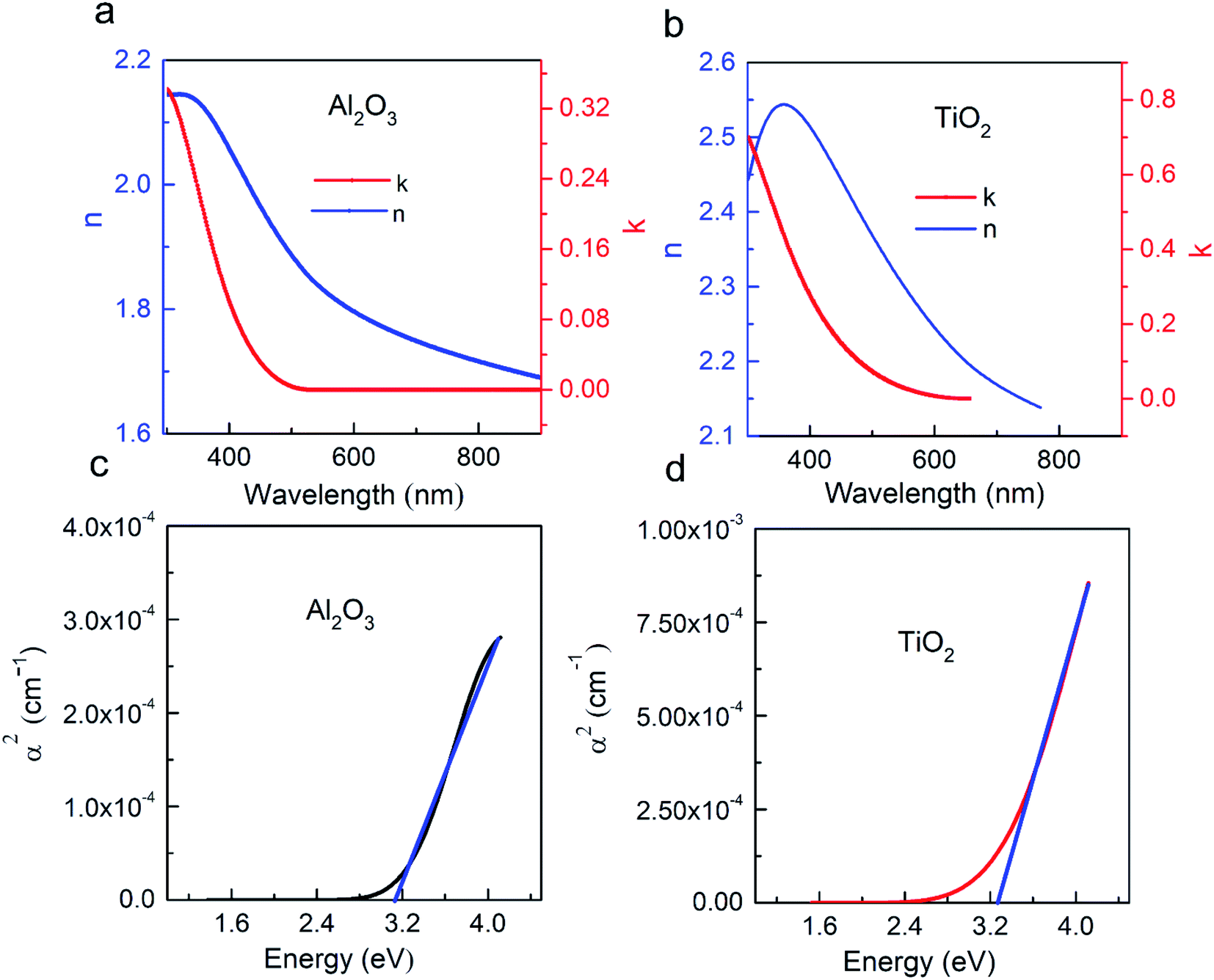
 Al2O3TiO2Al2O3TiO2Al2O3
 on glass substrate longwave pass edge filter at both the intensity values of transmission (%) show the same behavior. (d) Comparison of the performance of simulated (physical design) and experimental (fabricated) transmission (%) spectra versus wavelength (nm) in the 400–1000 nm range.
 Al2O3TiO2Al2O3TiO2 Al2O3
 longwave pass edge filter films were deposited alternately on the same substrates with different deposition times (30 min, 60 min) for each layer. The thickness of the bandpass filter by simulation was 293.12 nm and it was 328.2 nm in the experiment. The thickness of the longwave pass edge filter by simulation was 395.5 nm and it was 408.89 nm in the experiment. The maximum transmission of the 7-layer long wave pass edge filter was 99.73% in simulation and 54.60% in the experiment, and the reflectance of the 14-layer bandpass filter was 19% in simulation and 15% in the experiment. The difference in the transmission and reflectance in both the filters may be due to the increase in the thickness of individual or overall stack of layers for the Al2O3 and TiO2 thin films. Investigation of various material composites for manufacturing band pass, band stop, and narrow band pass filter for different applications was done and showed the advantage of the improved optical filters with low losses. The current work can be extended to the fabrication of beam splitters and reflective mirrors.