
 Open Access Article
 This Open Access Article is licensed under a Creative Commons Attribution-Non Commercial 3.0 Unported Licence
A planar ultraviolet objective lens for optical axis free imaging nanolithography by employing optical negative refraction†
Weijie
Kong‡
ab,
Ling
Liu‡
ab,
Changtao
Wang
ab,
Mingbo
Pu
ab,
Ping
Gao
a,
Kaipeng
Liu
ab,
Yunfei
Luo
ab,
Qijian
Jin
a,
Chengwei
Zhao
ab and
Xiangang
Luo
 *ab
*ab
aState Key Laboratory of Optical Technologies on Nano-Fabrication and Micro-Engineering, Institute of Optics and Electronics, Chinese Academy of Sciences, Chengdu 610209, China. E-mail: lxg@ioe.ac.cn
bSchool of Optoelectronics, University of Chinese Academy of Sciences, Beijing 100049, China
First published on 8th March 2022
Abstract
Lithography is one of the most key technologies for integrated circuit (IC) manufacturing and micro/nano-functional device fabrication, while the imaging objective lens plays one important role. Due to the curved surface of the conventional objective lens, the imaging field of view is limited and the objective lens system is complex. In this paper, a planar objective lens based on the optical negative refraction principle is demonstrated for achieving optical axis free and long depth of focus imaging nanolithography. Through employing a hyperbolic metamaterial composed of silver/titanium dioxide multilayers, plasmonic waveguide modes could be generated in multilayers, which results in optical negative refraction and then flat imaging at ultraviolet wavelength. The corresponding imaging characteristics are investigated in simulation and experiment. At the I-line wavelength of 365 nm, the highest imaging resolution of 165 nm could be realized in the 100 nm photoresist layer under the working gap of 100 nm between the objective lens and substrate. Moreover, this planar objective lens has good ability for cross-scale and two-dimensional imaging lithography, and is similar to a conventional projection objective lens. It is believed that this kind of planar objective lens will provide a promising avenue for low-cost nanofabrication scenarios in the near future.
Introduction
Almost all modern information technologies, such as Artificial Intelligence (AI), big data, 5G, and super-computing, are established on opto-electronic chips, and lithography provides the most efficient micro-/nano-manufacture approach. Current mainstream lithography technologies, such as deep ultraviolet (DUV)1,2 and extreme ultraviolet (EUV)3 lithography, critically depend on complex and cumbersome objective lens group systems, as well as expensive exposure sources. The main reason is that the conventional lens creates an image through a curved surface, when achieving a large numerical aperture (NA) and good imaging resolution, the thickness and weight of the optics would be increased drastically. Moreover, the aspheric surface of the lens lifts the difficulty and then the cost of lens fabrication. To simplify the design and fabrication of the lithography objective lens group, a planar lens is highly desirable. In recent years, the rise of Engineering Optics 2.0,4,5 which breaks the fundamental limitations of classic optical laws with respect to many aspects of optics (including reflection, refraction, diffraction, absorption and radiation, etc.) based on subwavelength structured materials, has facilitated the rapid progress of planar optics.6–8 As a representation of planar optics, the planar focusing lens starts with the perfect lens proposed by Pendry in 2000.9 By employing a negative refractive index material slab, a two-dimensional object could be imaged with subwavelength resolution in a point-to-point manner. As we know, a negative refractive index of materials means that the permittivity (ε) and permeability (μ) are all negative values, which shows the negative refraction of phase and power.10–12 In reality, if only considering the negative refraction of the propagation direction of light expected in the planar focusing lens, the conditions above could be relaxed and just the negative refraction of power is required. This indicates that optical negative refraction (power negative refraction) could be achieved without needing the material to have a negative refractive index. Currently, except for a positive uniaxial crystal,13 a uniaxially anisotropic material with a hyperbolic dispersion relation – commonly known as a hyperbolic metamaterial (HMM) has become a fascinating candidate for achieving optical negative refraction.14–16 Especially, a planar metal/dielectric single-periodic multilayer flat lens operating at ultraviolet (UV) wavelength was proposed,17 which demonstrates a clear focus in air 350 nm away from the surface of the flat lens through simulation and experiment. However, to the best of our knowledge, there are no reports about studies of planar UV objectives based on optical negative refraction for nanolithography applications.In this work, we report a planar UV objective lens for achieving optical axis free imaging nanolithography and alleviating the technical complexity of the objective lens of conventional projection lithography. Through employing a HMM consisting of a multilayer structure, planar negative refraction imaging lithography could be realized in the UV range. Because of the optical negative refraction effect, this objective lens does not have an optical axis. As a result, it possesses the capability for large area imaging without requiring the complex phase compensation often used by conventional projection lithography. At the I-line wavelength of 365 nm, the highest imaging lithography resolution of 165 nm has been reached in the Pr layer of 100 nm thickness in simulation and experiment under the air gap of 100 nm between the planar lens and substrate. Moreover, by critically adjusting the exposure parameters, cross-scale imaging lithography in a certain range could also be realized. Certainly, the two-dimensional (2D) imaging lithography capability is also verified by using the mask patterns of micro-rings. It is believed that this approach has potential applications in large area and near-diffraction limit lithography.
Results and discussion
As shown in Fig. 1(a), a planar lithography objective lens consists of 4 pairs of Ag (27 nm)/TiO2 (31 nm) unit cells and an extra Ag (27 nm) film is added as the outmost layer. The mask is composed of Cr patterns with a thickness of ∼60 nm, and is fabricated on a quartz substrate. The planar lithography objective lens and the mask are spaced by a PMMA layer with ∼35 nm thickness. The substrate is sapphire (Al2O3) coated with 100 nm photoresist (Pr) for printing the images of the mask. At the UV wavelength of 365 nm, the relative permittivity of Ag, TiO2, Cr, PMMA, Pr, sapphire and quartz is −2.6072 + 0.4145i, 8.0679 + 0.2695i, −8.5655 + 9.0072i, 2.25, 2.9095 + 0.1863i, 3.22 and 2.13, respectively. It is worth highlighting that the refractive index of the selected substrate should be larger than that of the Pr layer for preventing the waveguide effect, which would result in optical field fluctuation for line patterns.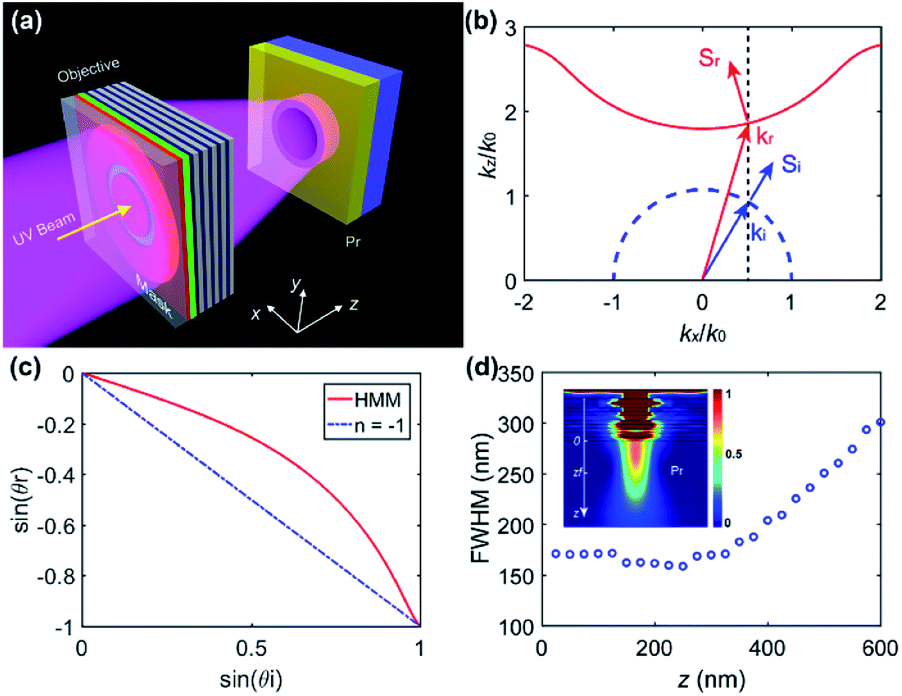 | ||
| Fig. 1 Planar lithography objective lens based on optical negative refraction. (a) Schematic of the planar objective lens. (b) Calculated EFCs for an ultraviolet plane wave of 365 nm in the as-designed periodic multilayer structure and in free space (k0 is the free space wave vector), the vertical dashed line represents the tangential wave vector component for conservation. (c) Sine of the Poynting vector refraction angle for the HMM and slab with n = −1 as a function of sine of the incident angle at the interface between the air and slab. (d) FWHM of the simulated lateral intensity profile of the image of a slit aperture of 180 nm along with the distance z away from the exit surface of the lens (z = 0). Inset is the intensity distribution in the xoz section. | ||
Under transverse magnetic (TM) polarization, the equifrequency contour (EFC) at 365 nm is calculated by the transfer matrix method,18 which is displayed in Fig. 1(b). When a plane wave illuminates the HMM from free space at a certain incident angle, due to the conservation of the transverse wave vector kx, the incident wave vector ki leads to the refractive wave vector kr which intersects with the EFC interface and the dashed line denotes the conserved transverse wave vector; kr points towards the EFC interface. The refractive Poynting vector Sr is normal to the tangent at the aforementioned intersection point, and it points away from the EFC interface. Obviously, the refractive Poynting vector Sr is oriented opposite the transverse direction of incident Poynting vector Si, which indicates power negative refraction. With regard to the phase front (kr), it still propagates in the positive transverse direction, which is similar to the transverse direction of the incident phase front (ki), and this indicates that the as-designed metamaterial could realize optical negative refraction without ensuring a negative phase index of refraction.12,19 As a matter of fact, the multilayer structure could be treated as an anisotropic medium by adopting the effective medium theory (EMT)20 and the effective permittivity along the x, y and z axis could be calculated as,21,22
| εxx = εyy = fεm + (1 − f)εd | (1) |
| εzz = εmεd/[(1 − f)εm + fεd] | (2) |
Because the hyperbolic EFC is not an ideal sphere, the refraction angle for the Poynting vector is a function of the incident angle, as depicted in Fig. 1(c). For the constant refractive index of n = −1, sin(θt) changes linearly with sin(θi), while for the proposed HMM, the relationship between sin(θt) and sin(θi) deviates from the linear one, where θi and θt are the incident angle and refraction angle for the Poynting vector, respectively. Fig. 1(d) shows the corresponding focusing effect of a single slit. The full-width at half-maximum (FWHM) of the focusing beam reduces with the distance away from the mask and reaches the minimum of 158.5 nm at a focal length zf of 250 nm. After that, the FWHM broadens drastically.
Then, the imaging capability for dense period lines is demonstrated for verifying the imaging resolution. In rigorous coupled wave analysis (RCWA)25 simulations, the grating pitch and duty cycle of the mask are set to 330 nm and 0.5, respectively. The duty cycle represents the proportion of the opaque area in the mask. The air gap between the planar lithography objective lens and substrate with the Pr layer is set to 100 nm. Fig. 2(a) displays the intensity distribution (|E|2) normalized by the incident intensity in the cross-section. It is evident that the dense line pattern of the mask is projected onto the Pr layer of the substrate in nearly 1![[thin space (1/6-em)]](https://www.rsc.org/images/entities/char_2009.gif) :1 without phase shift, which is different from the hyperlens having the capability of magnification/demagnification imaging26 and nanofocusing.27 The crosstalk between the adjacent fringe field is negligible and the exposure field penetrates the whole Pr layer of 100 nm thickness. Moreover, the normalized intensity profiles along the x direction in the different depths of the Pr layer are demonstrated in Fig. 2(b). It is apparent that the peak intensity of the image field decays with the depth of the Pr layer to some degree, but the contrast is always larger than 0.7, which ensures good exposure quality in the whole depth of the Pr layer. Additionally, the minimum normalized peak intensity approaches 0.08, this means that the exposure efficiency could reach ∼8.0%. The other energy is reflected and dissipated as heat due to the material loss.
:1 without phase shift, which is different from the hyperlens having the capability of magnification/demagnification imaging26 and nanofocusing.27 The crosstalk between the adjacent fringe field is negligible and the exposure field penetrates the whole Pr layer of 100 nm thickness. Moreover, the normalized intensity profiles along the x direction in the different depths of the Pr layer are demonstrated in Fig. 2(b). It is apparent that the peak intensity of the image field decays with the depth of the Pr layer to some degree, but the contrast is always larger than 0.7, which ensures good exposure quality in the whole depth of the Pr layer. Additionally, the minimum normalized peak intensity approaches 0.08, this means that the exposure efficiency could reach ∼8.0%. The other energy is reflected and dissipated as heat due to the material loss.
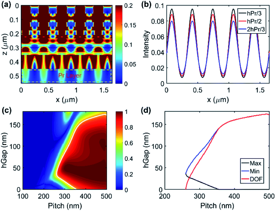 | ||
| Fig. 2 Negative refraction imaging simulations for periodical dense lines. (a) Normalized intensity distribution in the xoz section, and the yellow box displays the Pr layer. (b) Normalized intensity profiles at the different depths of the Pr layer. (c) Contrast of the imaging field in the center depth of the Pr layer for different working gaps and dense line pitches in the mask. The contrast contours of 0.7 are denoted by the white curves. (d) Maximum/minimum gap and the corresponding DOF as a function of the pitch of dense lines in the mask. The duty cycle of dense lines is 0.5. | ||
For negative refraction imaging lithography, the working gap between the planar objective lens and the substrate with the Pr layer plays the key role in lithography quality. Fig. 2(c) demonstrates the relationship between the contrast of the fringe field in the Pr layer and the pitch of dense lines of the mask, as well as the working gap. Herein, the contrast of the fringe field is defined as C = (Imax − Imin)/(Imax + Imin), where Imax and Imin are the peak and valley intensity in the middle depth of the Pr layer, respectively. For ensuring good exposure quality, the imaging contrast of 0.7 is used as the lithography criterion herein. At this condition, the minimum half-pitch of ∼165 nm could be achieved under the air working gap of ∼100 nm. This means that the highest half-pitch resolution reaches ∼165 nm, which is 1/2.21 of the exposure wavelength. One can see from Fig. 2(d), when the pitch of dense lines of the mask exceeds 330 nm and increases to 500 nm, the DOF improves monotonously, which effectively alleviates the difficulty of gap detection and control in the order of hundreds of nanometers. The simulated DOF for dense lines with a pitch of 330 nm, 350 nm, 410 nm and 500 nm is 106 nm, 135 nm, 162 nm and 172 nm, respectively. Considering the effect of the duty cycle of dense lines of the mask, the imaging DOF increases sharply at first and tends towards stability when the duty cycle exceeds 0.5, which is shown in Fig. S1 of the ESI.† The stable DOF is about 106 nm. In addition, as illustrated in Fig. S2 of the ESI,† for an identical working gap, the normalized peak intensity enhanced with increasing pitches of dense lines, and decreased with increasing duty cycles of dense lines. Overall, the energy efficiency of the negative refraction lithography objective lens along with the Pr layer is around ∼10%, which is an order of magnitude higher than deep subwavelength interference lithography utilizing HMM.28 With regard to one isolated line with a slit aperture of 180 nm, its image through the planar objective lens and the corresponding intensity profile along the cut line through the center are displayed in Fig. S3 of the ESI,† respectively. The FWHM is calculated and it is 170 nm.
The fabrication procedures of the planar UV objective lens as well as the mask are illustrated in Fig. 3 and the details are shown in the Experimental section. Once the objective lens with the mask and the substrate with the Pr layer were prepared, they were placed in the imaging lithography system29,30 to ensure near-field exposure.
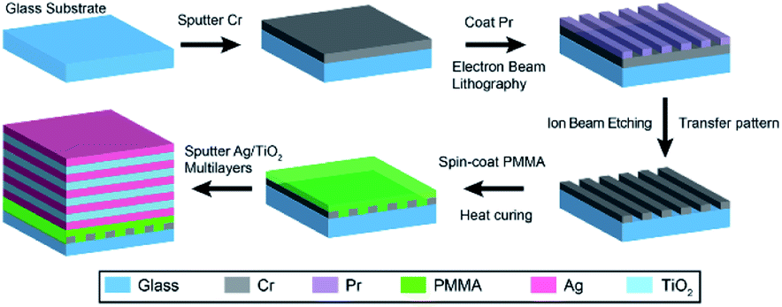 | ||
| Fig. 3 Schematic of the fabrication process of the planar lithography objective lens and mask. | ||
The surface characterization of the mask and cross-sectional view of the negative refraction imaging objective lens are exhibited in Fig. 4. Scanning electron microscopy (SEM) images of dense lines of the mask with nominal pitches of 330 nm, 350 nm, 410 nm and 500 nm are displayed in Fig. 4(a)–(d). The corresponding duty cycles of lines are 0.43, 0.44, 0.46 and 0.46, respectively. Meanwhile, Fig. S4 of the ESI† show the SEM images of dense lines of the mask with the nominal same pitch of 410 nm and different duty cycles of lines. The measured pitches are 415 nm, 408 nm and 409 nm, respectively, while the duty cycles of lines are 0.30, 0.46 and 0.55, respectively. For verifying the imaging lithography capability for 2D patterns, rings with the nominal same outer diameters of 2.0 μm and different ring widths are fabricated as mask patterns, which are shown in Fig. 4(e). The practical outer diameters are 2.02 μm and 2.05 μm, respectively. The corresponding ring widths are 480 nm and 390 nm, respectively. With respect to the cross-section characterization of the planar objective lens, the cross-sectional SEM image is clearly captured on spin-coated PMMA and Si wafer, as shown in Fig. 4(f). As designed, the thickness of the Ag film is ∼27 nm, while that of the TiO2 film is ∼31 nm.
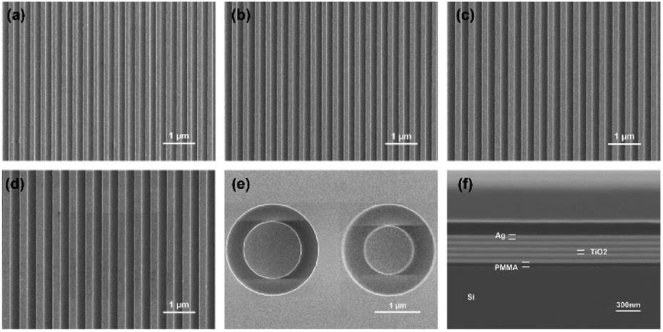 | ||
| Fig. 4 Mask patterns for imaging lithography. SEM images of dense lines of the mask with nominal pitches of (a) 330 nm, (b) 350 nm, (c) 410 nm and (d) 500 nm. (e) SEM image of rings of the mask with the nominal same outer diameters of 2.0 μm and different ring widths of 390 nm and 480 nm. (f) Cross-section view of the multilayer structure deposited on PMMA and Si wafer. | ||
After exposure and developing, the mask patterns are transferred to the Pr layer through a planar objective lens. Fig. 5 shows the SEM image of dense lines with 330 nm nominal pitch and the corresponding critical dimensions. The real mean line width and pitch of the mask are 143.1 nm and 330.5 nm, respectively. One can see that dense lines are maintained with high fidelity in the lithography process from Fig. 5(a). The corresponding line widths and pitches are extracted from the SEM image and displayed in Fig. 5(b). The line widths are 116.2 nm, 116.1 nm, 118.7 nm, 120.3 nm, 118.1 nm, 117.4 nm, 117.0 nm, 114.1 nm, 115.0 nm and 117.8 nm, respectively. The mean line width is 117.1 nm and the critical dimension uniformity (CDU) is ±2.73% (+2.73%/−2.56%). The mean pitch is 330.0 nm, which is nearly the same as that of the mask pattern. In short, under the present parameters, this planar objective lens could achieve the optimal resolution of ∼165 nm, which is consistent with the theoretical prediction. In addition, under identical conditions, the exposure result for one isolated line mask with a slit aperture of 180 nm is shown in Fig. S5 of the ESI,† and the measured line width is 298 nm, which is broadened due to the excess exposure dose.
 | ||
| Fig. 5 Exposure result for dense lines of the mask with 330 nm nominal pitch. (a) SEM image in the Pr layer. (b) Line widths and pitches of each line denoted by numbers in (a). | ||
Due to the fact that the integrated circuit layout contains patterns with different critical dimensions, the cross-scale lithography capability is highly desired for nanolithography methods. Fig. 6(a)–(c) shows dense line patterns in the Pr layer with different pitches under identical exposure and development conditions. It is obvious that the lines are distinguished clearly and pattern quality approaches the conventional lithography level. Quantitatively, the line widths and pitches are displayed in Fig. 6(d). The mean line width in the Pr layer for dense lines of the mask with a pitch of 330 nm, 350 nm, 410 nm and 500 nm is 117.1 nm, 117.2 nm, 156.7 nm and 172.4 nm, respectively. The corresponding CDUs are ±2.74%, ±3.12%, ±1.89% and ±1.16%, respectively, meeting the common requirement of within ±10%. Meanwhile, the mean pitches of Pr patterns are 330.0 nm, 347.7 nm, 410.4 nm and 509.0 nm, respectively, which approach the corresponding mask pitches. These results demonstrate that this planar objective lens based on optical negative refraction also has the cross-scale imaging lithography capability.
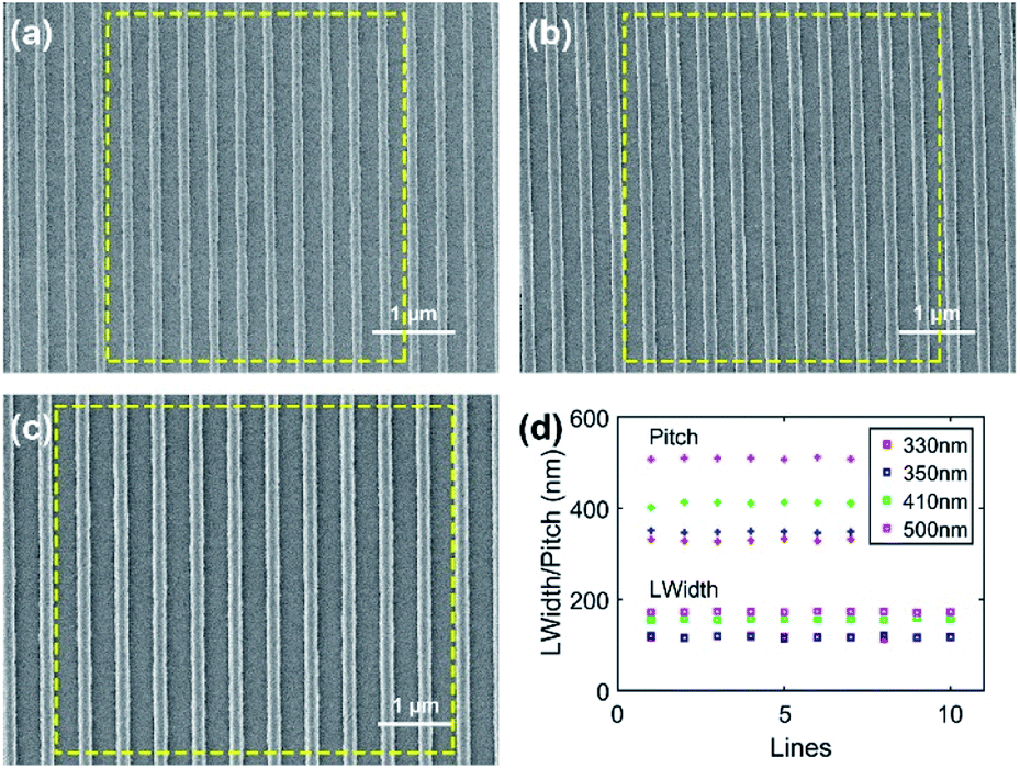 | ||
| Fig. 6 Exposure result for the dense lines of the mask with 350 nm, 410 nm and 500 nm nominal pitches. (a)–(c) The corresponding SEM images in the Pr layer. (d) Line widths and pitches of each line in yellow boxes in (a)–(c). | ||
Under the conditions of identical mask pitch and exposure dose, the line width in the Pr layer could be adjusted by changing the duty cycle of dense lines in the mask, which has been validated in Fig. 7(a)–(c). With an increase in the duty cycle of mask patterns from 0.30 and 0.46 to 0.55, the mean line width in Pr improves from 164.5 nm and 236.5 nm to 293.1 nm drastically, while the mean pattern pitch fluctuates around 400 nm. It is noteworthy that the effective exposure dose for the Pr layer would reduce with the increase of duty cycle of mask patterns, while the imaging contrast remains larger than 0.8 when the duty cycle is in the range of 0.33 to 0.93, as shown in Fig. S6 of the ESI.† This leads to insufficient exposure in the large duty cycle of mask patterns and then comparatively distorted lines in the Pr layer, as depicted in Fig. 7(c). The problem could be resolved by enhancing the exposure dose illuminating the mask for the patterns with a large duty cycle. Moreover, for the sake of observing lines after exposure stereoscopically, the substrate with the Pr layer is inclined by 20° in SEM and the stereoscopic image of patterns in Pr is captured, as shown in Fig. 7(d). The line edges seem to be steep in depth and the line edge roughness (LER) may be slight. This is a direct consequence of the long DOF and large imaging contrast of the planar objective lens.
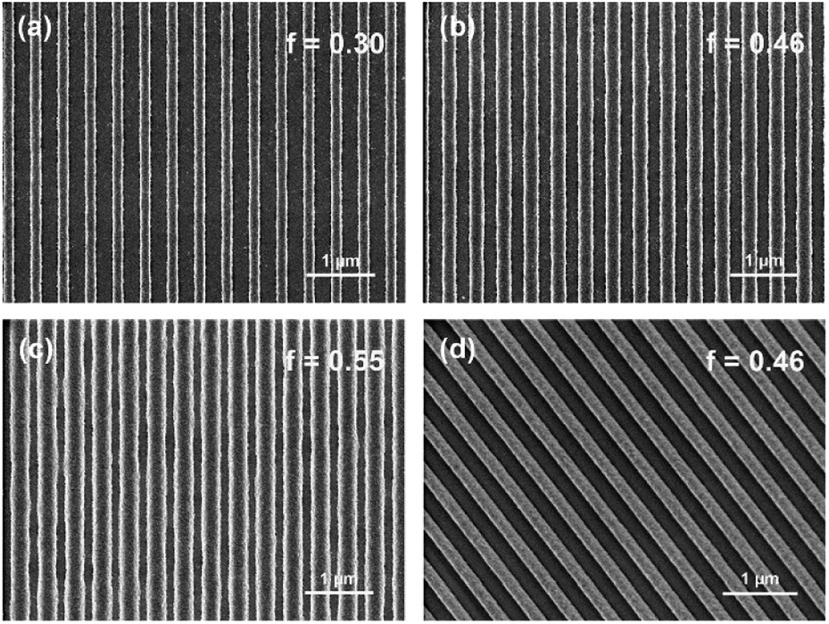 | ||
| Fig. 7 Exposure result for the dense lines of the mask with the nominal same pitch of 410 nm and different duty cycles of lines of (a) 0.30, (b) 0.46 and (c) 0.55 in the Pr layer. (d) Stereoscopic image of (b). | ||
Although the above discussions and results focus on one-dimensional lines, this planar objective lens also has the ability to image any 2D patterns, which is similar to the conventional projection objective lens. We employ two micro-ring patterns with nominal same outer diameters of 2.0 μm but different ring widths of 480 nm and 390 nm for validating the 2D imaging lithography ability. Based on the Hopkins approximate, the TE and TM modes of the unpolarized source could be approximated to have constant directions along two orthogonal axes.31,32 Therefore, image field intensity distributions are approximated as the superposition of that under the TE and TM polarized illumination. Fig. 8(a) and (c) show the image field intensity (|E|2) distributions in the middle depth of the Pr layer for two micro-rings under an unpolarized source. One can see that annular field intensity distributions are generated. For two micro-rings, the peak intensities are not the same (0.076/0.063 for micro-rings with ring widths of 480 nm/390 nm) due to the different ring widths, which are shown in Fig. 8(b) and (e) more clearly. This means that the exposure dose and duration need to be adjusted for each case. After exposure and developing, the patterns in Pr layer are obtained and the SEM images are displayed in Fig. 8(c) and (f). Obviously, the mask patterns are transferred to the Pr layer with high fidelity in experiments. The measured outer/inner diameters for micro-rings in the Pr layer are 2.00 μm/1.00 μm and 2.00 μm/1.18 μm, respectively. That is, the corresponding ring widths are 500 nm and 410 nm. In comparison with the mask patterns, the ring widths in the Pr layer increase by ∼20 nm for 480 nm and 390 nm ring widths of mask patterns, respectively. This may result from the fact that over-exposure took place and the ring widths are broadened in the lithography process. Through critically controlling the exposure dose, this problem would be addressed along with the improvement of the near-field lithography system.
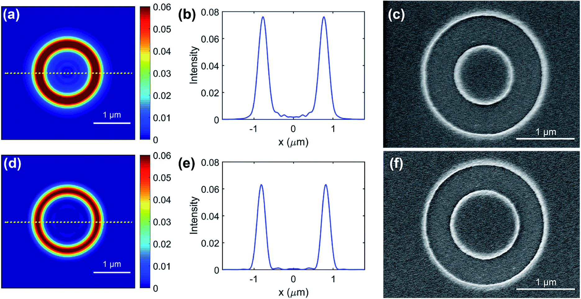 | ||
| Fig. 8 Imaging and exposure results for two micro-rings with nominal same outer diameters of 2.0 μm but different ring widths of 480 nm and 390 nm. (a) Image field intensity distribution, (b) intensity profile along the cut line through the center, and (c) SEM image in the Pr layer for a micro-ring with 450 nm ring width. (d)–(f) Same as (a)–(c) but with 390 nm ring width. | ||
Compared with the famous superlens,33–36 the imaging mechanism and imaging effect of this negative refraction imaging objective lens are notably different. The superlens enhances the evanescent wave component of the object through exciting surface plasmons and sub-diffraction imaging capability could be achieved. Because of the exponential decay of the evanescent wave component, the working distance between the superlens and image plane is often in the order of ten nanometers. The direct consequence is that it is difficult to realize uniform nano-gap control between the superlens and wafer for achieving large area lithography. Alternatively, the negative refraction imaging objective lens employs excited surface plasmons in the metal-dielectric alternatively stacked multilayer structure for realizing optical negative refraction. The working distance between the objective lens and wafer could be enlarged to some extent, which would relieve the rigorous demand of gap control and wafer surface distribution to some degree. Of course, sub-diffraction imaging lithography could not be reached due to the loss of the most evanescent wave component carrying subwavelength information of the object at present. In essence, this negative refraction imaging objective lens is a counterpart of the conventional projection imaging objective lens37 composed of dozens of lenses with nano-precision in the curved surface shape and lens position. Due to the curved surface of the objective group, its imaging FOV is limited, while, for the planar lithography objective lens based on optical negative refraction, there is no optical axis when imaging, which is typical of a linear shift invariant system (LSIS). This means that the unlimited imaging FOV could be reached when supposing that the surfaces of lens and wafer are flat, as well as the gap between lens and wafer is uniform. In addition, the manufacture complexity and cost of the negative refraction lithography objective lens would be reduced. In addition, the particle lens array38 could also achieve a comparatively long working distance for micro/nano fabrication, but the resolution and FOV are limited.
Conclusions
In conclusion, we demonstrated a planar objective lens for long DOF and optical axis free UV imaging nanolithography. This planar objective lens is composed of Ag/TiO2 multilayers and belongs to the type-I HMM. By launching plasmonic waveguide modes in stacked multilayers, optical negative refraction would appear, which leads to flat imaging capability. Under 365 nm wavelength illumination, the imaging resolution could reach 165 nm and the corresponding DOF of 106 nm could be realized. Because the working distance could be enlarged to 100 nm, the nano-gap detecting and controlling between the planar objective lens and wafer would be relieved. Meanwhile, the cross-scale imaging lithography capability in the range of 330–500 nm is demonstrated through single exposure, and flexible line width control is also realized in the Pr layer. Moreover, the imaging ability for 2D patterns is also verified through exposure experiments for micro-rings. In other words, the proposed planar objective lens could supply another option for large scale nanolithography.Experimental section
Numerical simulations
Three-dimensional simulations were performed using Lumerical® FDTD Solutions 2020, while two-dimensional simulations and calculations were conducted using MATALB® R2016b.Sample preparation
A Cr layer with a thickness of 60 nm was deposited on a quartz substrate by magnetron sputtering. Subsequently, the commercial positive e-beam resist, AR-P 6200.04 (ALLRESIST GmbH, Strausberg) was spin-coated on the Cr layer. After electron beam lithography (EBL) and the subsequent inductively coupled plasma (ICP) etching, masks with various patterns were produced after cleaning the e-beam resist. Next, a PMMA layer with a thickness of 120 nm was spin-coated on the mask at 4000 rpm for 30 s, and baked for 60 min at 120 °C in an oven to solidify PMMA. Then, reactive ion etching (RIE) was adopted to reduce the thickness of the PMMA layer to about 35 nm, which serves as the planar and spacing layer between the mask and objective lens. After that, multilayers made of alternating 27 nm Ag and 31 nm TiO2 were deposited on the planar PMMA layer by magnetron sputtering (DE500, DE Technology Limited), and the deposition rates were 0.415 nm s−1 for Ag and 0.046 nm s−1 for TiO2, respectively. For preparing the sapphire substrate with a spacer in its edge, a positive Pr (AZ3100) with 1 μm thickness was spin-coated, followed by UV exposure (60 s). Then, the exposed area was etched by ion beam etching (IBE) at a rate of 3.5 nm min−1 and the unexposed positive Pr as the protective layer was cleaned with acetone after etching. Finally, an AR-3170 positive Pr (ALLRESIST GmbH, Strausberg) layer with a thickness of 100 nm was spin-coated on the etched substrate and then spacers with a height of ∼80 nm on substrate edges were fabricated.Lithography process
A home-built near-field lithography system was used for lithography experiments. Under the pressure from airflow (0.7 MPa), a highly intimate interaction between the substrate with the spacer and multilayers was realized, and the gaps were close to ∼100 nm except for the spacer area which had gaps of ∼20 nm. Collimated UV light with 365 nm wavelength from a mercury lamp illuminates the mask through a linear polarizer. The light power was set at 7.1 mW cm−2, and the exposure lasted for 300 s. After relaxing pressure, the Pr layer on the substrate was immersed in 1:1 diluted AR-300-35 developer for ∼20 s, followed by a 30 s deionized (DI) water rinse and nitrogen drying, respectively.
Author contributions
The manuscript was written through contributions of all authors. All authors have given approval to the final version of the manuscript.Conflicts of interest
There are no conflicts to declare.Acknowledgements
This work was supported by the National Natural Science Foundation of China (No. 62005288 and 62192773), and Youth Innovation Promotion Association CAS (No. 2021379).References
- S. J. Holmes, P. H. Mitchell and M. C. Hakey, IBM J. Res. Dev., 1997, 41, 7–19 CAS.
- Y. Wei and R. L. Brainard, Advanced Processes for 193-nm Immersion Lithography, SPIE press, 2009 Search PubMed.
- V. Bakshi, EUV Lithography, SPIE Press, 2009 Search PubMed.
- X. Luo, ACS Photonics, 2018, 5, 4724–4738 CrossRef CAS.
- X. Luo, Adv. Mater., 2019, 31, 1804680 CrossRef PubMed.
- P. Genevet, F. Capasso, F. Aieta, M. Khorasaninejad and R. Devlin, Optica, 2017, 4, 139–152 CrossRef CAS.
- Y. Wang, Q. Fan and T. Xu, Opto-Electron. Adv., 2021, 4, 200008 CAS.
- Y. Zhu, X. Chen, W. Yuan, Z. Chu, K.-y. Wong, D. Lei and Y. Yu, Opto-Electron. Adv., 2021, 4, 210013 CAS.
- J. B. Pendry, Phys. Rev. Lett., 2000, 85, 3966–3969 CrossRef CAS PubMed.
- T. Xu, A. Agrawal, M. Abashin, K. J. Chau and H. J. Lezec, Nature, 2013, 497, 470–474 CrossRef CAS PubMed.
- I. Aghanejad, K. J. Chau and L. Markley, Phys. Rev. B, 2016, 94, 165133 CrossRef.
- E. Verhagen, R. de Waele, L. Kuipers and A. Polman, Phys. Rev. Lett., 2010, 105, 223901 CrossRef PubMed.
- Y. Zhang, B. Fluegel and A. Mascarenhas, Phys. Rev. Lett., 2003, 91, 157404 CrossRef PubMed.
- D. Lee, S. So, G. Hu, M. Kim, T. Badloe, H. Cho, J. Kim, H. Kim, C.-W. Qiu and J. Rho, eLight, 2022, 2, 1–23 CrossRef.
- H. Cho, S. So, T. Badloe, S. Bang and J. Rho, Adv. Theory Simul., 2020, 3, 2000138 CrossRef CAS.
- H. Cho, Y. Yang, D. Lee, S. So and J. Rho, Nanophotonics, 2021, 10, 3871–3877 CrossRef.
- R. Maas, J. van de Groep and A. Polman, Optica, 2016, 3, 592–596 CrossRef CAS.
- P. Yeh, Optical Waves in Layered Media, Wiley, New York, 1988 Search PubMed.
- J. Yao, K. Tsai, Y. Wang, Z. Liu, G. Bartal, Y. L. Wang and X. Zhang, Opt. Express, 2009, 17, 22380–22385 CrossRef CAS PubMed.
- D. Aspnes, Am. J. Phys., 1982, 50, 704–709 CrossRef.
- B. Wood, J. Pendry and D. Tsai, Phys. Rev. B: Condens. Matter Mater. Phys., 2006, 74, 115116 CrossRef.
- O. Kidwai, S. V. Zhukovsky and J. Sipe, Phys. Rev. A: At., Mol., Opt. Phys., 2012, 85, 053842 CrossRef.
- Y. Guo, W. Newman, C. L. Cortes and Z. Jacob, Adv. OptoElectron., 2012, 2012, 452502 Search PubMed.
- M. Lee, E. Lee, S. So, S. Byun, J. Son, B. Ge, H. Lee, H. S. Park, W. Shim and J. H. Pee, J. Am. Chem. Soc., 2021, 143, 20725–20734 CrossRef CAS PubMed.
- M. Moharam and T. Gaylord, J. Opt. Soc. Am., 1981, 71, 811–818 CrossRef.
- J. Rho, Z. Ye, Y. Xiong, X. Yin, Z. Liu, H. Choi, G. Bartal and X. Zhang, Nat. Commun., 2010, 1, 1–5 CAS.
- M. Kim, S. So, K. Yao, Y. Liu and J. Rho, Sci. Rep., 2016, 6, 1–6 CrossRef PubMed.
- G. Liang, C. Wang, Z. Zhao, Y. Wang, N. Yao, P. Gao, Y. Luo, G. Gao, Q. Zhao and X. Luo, Adv. Opt. Mater., 2015, 3, 1248–1256 CrossRef CAS.
- W. Kong, Y. Luo, C. Zhao, L. Liu, P. Gao, M. Pu, C. Wang and X. Luo, ACS Appl. Nano Mater., 2019, 2, 489–496 CrossRef CAS.
- M. Liu, C. Zhao, Y. Luo, Z. Zhao, Y. Wang, P. Gao, C. Wang and X. Luo, J. Vac. Sci. Technol., B: Nanotechnol. Microelectron.: Mater., Process., Meas., Phenom., 2017, 35, 011603 Search PubMed.
- J. T. Azpiroz, Analysis and modeling of photomask near-fields in sub-wavelength deep ultraviolet lithography with optical proximity corrections, PhD dissertation, University of California, 2004.
- K. Adam, Domain decomposition methods for the electromagnetic simulation of scattering from three-dimensional structures with applications in lithography, PhD dissertation, University of California, 2001.
- N. Fang, H. Lee, C. Sun and X. Zhang, Science, 2005, 308, 534–537 CrossRef CAS PubMed.
- Z. Zhao, Y. Luo, W. Zhang, C. Wang, P. Gao, Y. Wang, M. Pu, N. Yao, C. Zhao and X. Luo, Sci. Rep., 2015, 5, 15320 CrossRef CAS PubMed.
- P. Gao, N. Yao, C. Wang, Z. Zhao, Y. Luo, Y. Wang, G. Gao, K. Liu, C. Zhao and X. Luo, Appl. Phys. Lett., 2015, 106, 093110 CrossRef.
- K. Huang, F. Qin, H. Liu, H. Ye, C. W. Qiu, M. Hong, B. Luk'yanchuk and J. Teng, Adv. Mater., 2018, 30, 1704556 CrossRef PubMed.
- J. H. Bruning, Optical Microlithography XX, International Society for Optics and Photonics, 2007, 6520, p. 652004 Search PubMed.
- Z. Wang, W. Guo, A. Pena, D. Whitehead, B. Luk'Yanchuk, L. Li, Z. Liu, Y. Zhou and M. Hong, Opt. Express, 2008, 16, 19706–19711 CrossRef CAS PubMed.
Footnotes |
| † Electronic supplementary information (ESI) available: Fig. S1–S6. See DOI: 10.1039/d1na00883h |
| ‡ These authors contributed equally to this work. |
| This journal is © The Royal Society of Chemistry 2022 |