
 Open Access Article
 This Open Access Article is licensed under a Creative Commons Attribution-Non Commercial 3.0 Unported Licence
Experimental determination of the lateral resolution of surface electric potential measurements by Kelvin probe force microscopy using biased electrodes separated by a nanoscale gap and application to thin-film transistors
Mélanie
Brouillard†
ab,
Nicolas
Bercu†
a,
Ute
Zschieschang
b,
Olivier
Simonetti
a,
Rakesh
Mittapalli
 a,
Hagen
Klauk
b and
Louis
Giraudet
*a
a,
Hagen
Klauk
b and
Louis
Giraudet
*a
aLaboratoire de Recherche en Nanosciences (LRN EA 4682), Université de Reims Champagne-Ardenne, 51100 Reims, France. E-mail: louis.giraudet@univ-reims.fr
bMax Planck Institute for Solid State Research, Stuttgart, Germany
First published on 22nd March 2022
Abstract
A method is proposed to estimate the lateral resolution of surface potential profile measurements using Kelvin probe force microscopy (KPFM) on operating electronic devices. De-embedding the measured profile from the system response is required for various applications, such as contact characterization of thin-film transistors, or local longitudinal electric field measurements. A method is developed based on the measurement of the electric potential profile of two metallic electrodes separated by a nano-gap, providing a quasi-planar configuration. The electrodes are independently biased so as to produce an abrupt and well-controlled potential step. This calibration sample is used to measure the system impulse response in various configurations. Due to the application constrains, the KPFM method employed here is based on a dual-pass mode, demonstrated to provide reliable measurements on operating electronic devices. The method is applied to two types of conductive AFM probes. Measurements are performed at different tip-to-sample heights allowing the determination of the lateral resolution of the double-pass method. Detailed description of the measurements and resolution results are given for the present KPFM configuration. The system resolution measurement technique can be extended to other KPFM modes and can be used to monitor the degradation of the tip quality during long measurement campaigns. Finally, the method is applied to the characterization of thin-film transistors, and the effects of contact edge sharpness on the device behavior is discussed. The longitudinal electric field responsible for charge injection at the source-contact edge is successfully estimated and compared for organic thin-film transistors fabricated by stencil lithography or electron-beam lithography.
Introduction
An important requirement for Kelvin probe force microscopy (KPFM), as for most scanning probe microscopy (SPM) techniques, is to have a good estimate of the lateral resolution, in the case of KPFM of the measured surface potential profile. The lateral resolution reflects the ability of the measurement method to spatially separate the contributions of different electrostatic sources present in the sample. It is much more difficult to estimate the lateral resolution in KPFM than in SPM topography measurements where the tip apex diameter is the determining factor.The double-pass method in amplitude-modulated (AM) KPFM2–4 was initially proposed in order to provide the ability to distinguish the long-range electrostatic forces from the short-range van der Waals interaction. However, the simultaneous contributions of the tip and the cantilever to the long-range electrostatic interaction make it impossible to estimate the local surface potential in a straightforward manner.5 To eliminate these problems, KPFM based on frequency modulation (FM) and phase modulation (PM) will be discussed in the present work.1,3
The lateral resolution of KPFM measurements has been discussed in many previous publications,6–15 and several definitions have been proposed. Some authors have measured the response of the system to a potential step and have defined the resolution as the distance traveled by the tip to measure a certain percentage of the applied potential difference.6,7 Others estimate the radius of a circular surface area centered below the tip that accounts for half of the total electrostatic tip–sample interaction.8 This latter method is more suited to a theoretical determination of the resolution. However, any definition of the resolution has to deal with the fact that the surfaces on which the measurements are performed are usually not flat and that the effects of the topography on the measurement results are difficult (if not impossible) to formalize. This greatly complicates any general assessment of the KPFM resolution. Despite these difficulties, it remains relevant to measure the response of the system in a given experimental configuration, targeting a given application, opening the way to a precise analysis of the measured surface potential profiles in that configuration and to the understanding of the device under study.
In the application targeted in the present study, i.e., the characterization of thin-film transistors, the device is mostly planar with limited topography, and the surface potential profile is measured along the semiconductor channel from the source contact to the drain contact. The surface potential profile is asymmetric, as the potential is constant in the direction perpendicular to the semiconductor channel (parallel to the contact edges), but varies greatly along the channel (from source to drain). The proposed resolution evaluation method has been developed considering this characteristic asymmetry and is performed in a configuration similar to that of a thin-film transistor.
For the sake of simplicity, the KPFM resolution is defined here as the full width at half maximum (FWHM) of the system impulse response to a unidirectional Dirac-type excitation, approximated to a Gaussian.9 This method uses a principle that is identical to the one employed in conventional microscopy using the Rayleigh criterion.10 Since devices presenting a Dirac potential profile are difficult to implement experimentally, a dedicated calibration sample consisting of pairs of metal electrodes separated by a narrow gap has been designed and fabricated to be able to produce a well-defined in-plane potential step over a very short lateral distance of approximately 10 nm. As described in the following, this approach provides a robust and reliable estimate of the lateral resolution of the surface potential measurement. The technique is independent of the conductive cantilever employed for the measurement and can be used in situ to monitor the degradation of the tip quality during long measurement campaigns, as will be demonstrated below.
Calibration-device structure and fabrication
Dedicated calibration devices were designed and fabricated using electron-beam lithography,16 as depicted in Fig. 1. A 100 nm-thick layer of Al2O3 was deposited onto a silicon substrate by atomic layer deposition, followed by the deposition of poly(methyl methacrylate) as an electron-beam resist. In addition to designing seven different intended gap lengths (20, 30, 40, 50, 60, 80 and 100 nm), electron-beam lithography was performed using four different exposure doses (900, 1100, 1300 and 1500 μC cm−2; JEOL JBX6300FS), with the intention of obtaining the smallest possible electrode spacing. After resist exposure and development, a 0.3 nm thick layer of titanium (to promote adhesion) followed by a 22 nm thick layer of gold/palladium were deposited by thermal evaporation in vacuum and patterned by lift-off.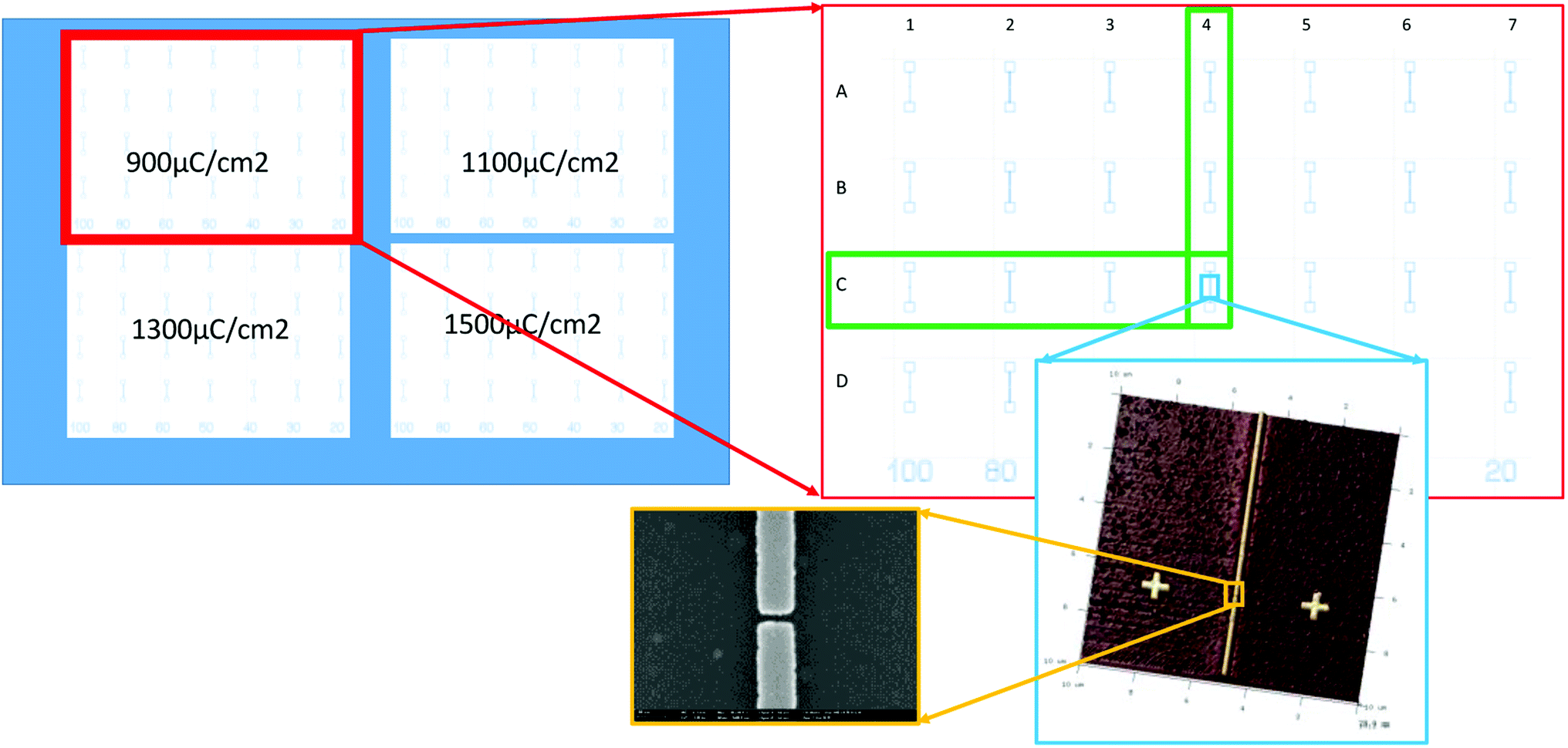 | ||
| Fig. 1 Layout of calibration devices to experimentally determine the lateral resolution of the surface potential profile measured by Kelvin probe force microscopy (KPFM). Each calibration device consists of a pair of metal electrodes separated by a gap defined by electron-beam lithography. Lithography was performed using exposure doses of 900, 1100, 1300 and 1500 μC cm−2. The designed gap lengths range from 20 to 100 nm, and the smallest obtained gap length (measured by SEM) is 12 nm. | ||
The gap lengths measured by scanning electron microscopy (SEM) range from 12 nm to 84 nm.
Experimental KPFM setup
A commercial atomic force microscope (Bruker Dimension Icon) was adapted in order to perform quantitative surface-potential measurements on operating thin-film transistors.1,3 The experimental method relies on a conductive probe placed at the end of a flexible cantilever. The conductive tip interacts with the surface due to electrostatic forces. Monitoring the attractive force makes it possible to measure the surface potential.4 To maximize the robustness of the measurements for the targeted application, i.e., the in situ measurement of active electronic devices, biased at voltages well in excess of 10 V, a dual-pass KPFM mode (lift mode) was employed.2 The overall technique is illustrated in Fig. 2. It consists of two successive scans for each line, in order to separate the short-range interaction forces, such as van der Waals forces, from the long-range electrostatic interaction,4 and to allow the device to be biased exclusively in lift mode.1 During the first line scan (round trip), the system records the surface topography while all biases (device and tip) are zeroed. During the second scan, the tip is lifted up to a user-defined height, typically a few tenths of nanometers, and follows the previously recorded surface profile. During this second pass, the device under study is biased as desired, and the resulting surface potential profile is measured. For greater reliability and equipment safety in case of accidental contact of the tip with the sample surface, a fast current-compliance management is performed by applying the bias voltages to both the operating device and the AFM tip using the same voltage source (Keysight E5270B). This method has been demonstrated to be reliable and robust, providing quantitative surface potential measurements on operating transistors biased with gate-source and drain-source voltages exceeding 30 V in ambient conditions.1 Since using a double pass method is not without impact on the KPFM lateral resolution, after a description of the experiment, resolution issues will be discussed.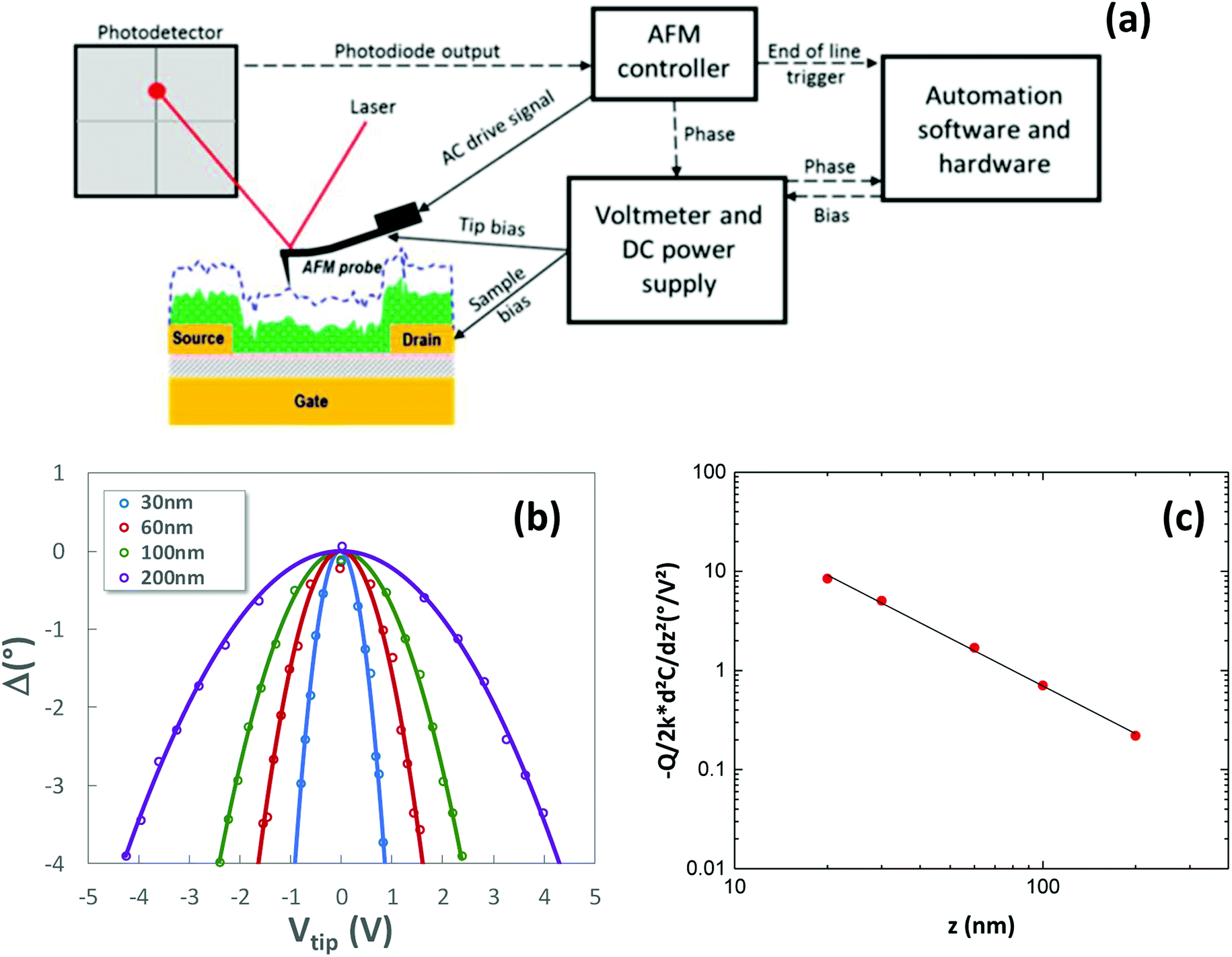 | ||
| Fig. 2 (a) Schematics of the KPFM setup and illustration of the lift mode during the measurement of the surface potential profile of a thin-film transistor. (b) Measured phase shift versus tip bias at various lift heights. (c) Variation of the parabola opening versus the lift height. AFM tip: Bruker SCM-PIT-V2. The experimental power law is −1.60 ± 0.04. | ||
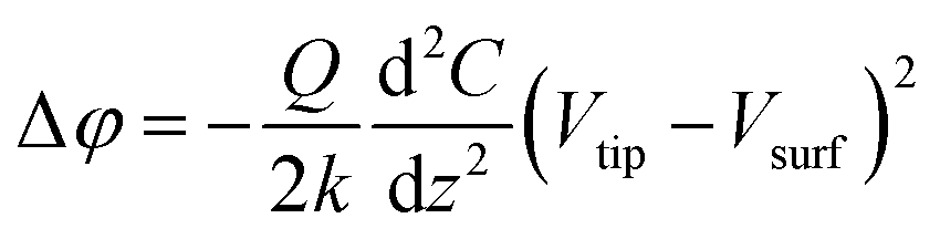
During the lift scan, an external digital phase-control loop1,3 makes it possible to quantitatively measure the surface potential. The phase-shift control loop is based on the measurement of the phase difference Δφ between the cantilever excitation drive AC signal and the actual cantilever oscillation signal measured by the photodetector. Within a limited tip-to-surface potential difference (Vtip − Vsurf), as illustrated in Fig. 2(b), the electrostatic interaction between the tip and the surface produces a phase shift of the cantilever oscillation, which can be described by a parabola:7
 | (1) |
 is the phase parabola opening, with Q being the quality factor and k the spring constant of the cantilever. The phase parabola opening is proportional to the second derivative of the capacitance,
  , which is dependent on the parameter z, as shown in Fig. 2(b) and (c). Since the phase shift depends on the electrostatic force gradient,7 the technique minimizes the influence of the cantilever and provides a resolution similar to frequency-modulation KPFM modes.17 The maximum of the parabola is obtained when the tip bias Vtip equals the local surface potential Vsurf (Fig. 2(b)). The continuous acquisition of the phase parabola while scanning makes it possible to measure the surface potential along the transistor channel.
A maximum phase shift of 4° is targeted during the numerical feedback loop. This prevents the electrostatic forces to be applied to the cantilever from being too large. The maximum cantilever deflection was measured in standard conditions during the phase feedback loop. For lift heights ranging from 30 nm and 200 nm, the deflection was found to be below 3% of the lift heights for the SCMPIT-V2 and the PFQNE-AL probes. This limited cantilever deflection is thought to not influence the surface potential measurements.
As shown in Fig. 2(b) the phase parabola opening decreases when the lift height increases, since the electrostatic interaction between the tip and the surface decreases. This decrease was found to follow a power law dependence, as shown in Fig. 2(c) for the SCMPIT-V2 probes, with a slope of −1.60 ± 0.04. This slope agrees with the model and experimental results of S. Belaidi et al.18 at intermediate lift distances, with a power law dependence of the force gradient between −1 and −2 at comparable lift heights. Furthermore, at a lift height of 30 nm, the experimental phase opening is close to that predicted by the sphere model expression 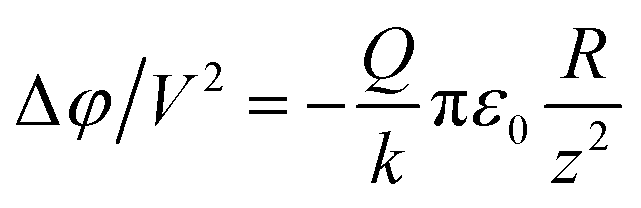 with R the tip radius, and z the lift height. A tip radius of 30 nm is calculated from this equation, compared to the nominal value of 25 nm. This model should only be valid for lift heights that are small compared to the tip radius (z ≪ R); under these conditions the power law dependence should be −2, i.e., the force gradient should vary as 1/z2. On the other extrema of our experimental data, i.e., for a lift height of 200 nm and using the PFQNE-AL tips with a radius of 5 nm, the phase parabola opening of 0.22° V−2 matches well with the uniformly charge line model developed in ref. 19, giving 0.25° V−2 when approximating the PFQNE-AL tip cone angle to 20°. Following this model, the power law dependence of the force gradient with the lift height should be −1, varying as 1/z. At intermediate lift heights, our data suggest an intermediate situation between these two models, with a power law of −1.6.
Resolution estimate of the double-pass KPFM method
In the framework of the Jacobs model,20 the surface potential expression is generalizable when the potential evolves in the form of a two-dimensional convolution product between the surface potential, assumed to be flat, and the probe point spread function (PSF). In the present work, we target the measurement of the potential profiles of thin-film transistors. These devices exhibit an almost invariant structure along one axis (y), in the direction parallel to the edges of the source and drain contacts (having a width of 200 μm), and a ‘limited’ topography (discussed below). The problem is therefore reduced to a one-dimensional problem along the scan direction (x), in particular neglecting any surface topography related effects. In our system, we demonstrate below that the system resolution is not only dependent on the probe PSF, but also on the phase feedback loop. The measured potential therefore results from the convolution of three contributions, namely the surface potential, the probe PSF, and the phase feedback loop.Thanks to the properties of the convolution product, the KPFM measurement system impulse response can be expressed as a function g(x) being the convolution of the probe PSF with the phase feedback loop impulse response, as illustrated in Fig. 3. The measured electrical potential Vmeas at a given point xprobe of the tip above the surface can be written as:
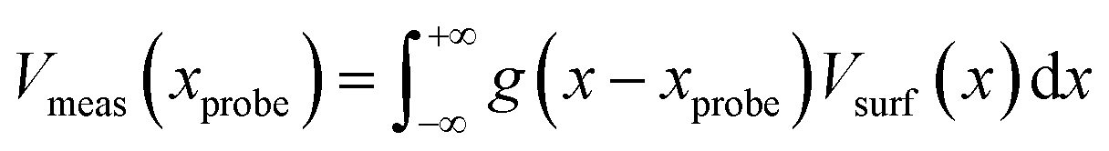 | (2) |
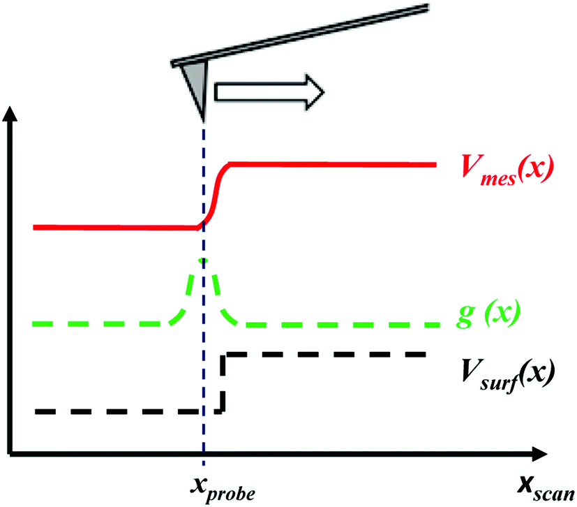 | ||
| Fig. 3 Illustration of the principle of the method to experimentally determine the lateral KPFM system resolution. The measured surface potential (full red line) is a convolution of an ideal (perfectly abrupt) potential step (black dashed line) and the system response function g(x) (green dashed line). The lateral resolution of the system is defined as the FWHM of g(x). | ||
The measured potential Vmeas at a given position xprobe along the scan line depends on the surface potential Vsurf(x) convolved by the function g(x). This formulation is valid only if the sample has limited topography.
Theoretical studies show that the tip/sample capacitance and the system impulse response g(x) are very sensitive to the shape of the tip, in particular its apex, and to the actual scan height.21 In practice, the tip shape can evolve during the measurement, because of wear, or due to in situ tip contamination. There is a justified interest in measuring the effective system impulse response for various tip–sample configurations in order to define the best measurement conditions and to monitor the system.
To measure the system impulse response, we have used the dedicated devices described above, consisting of two metal electrodes separated by a nanometric gap (Fig. 4).
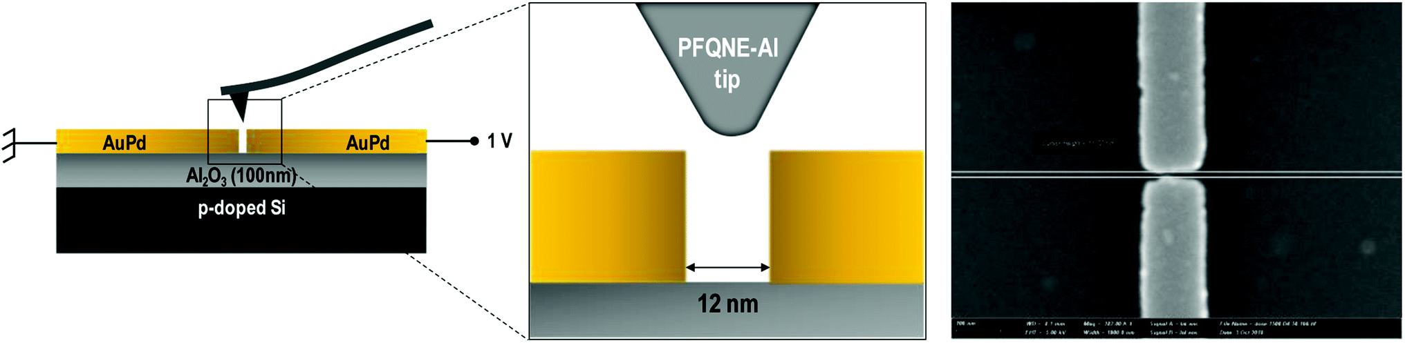 | ||
| Fig. 4 Left: schematic cross section of a calibration device with an AFM tip in proximity. Scales are adapted to the PFQNE-AL tip above the 12 nm gap, with 22 nm-thick AuPd electrodes. Right: SEM image of a calibration device with a gap length of 12 nm. | ||
During the experiment, the two metal electrodes are biased independently to achieve an abrupt potential drop of typically 1 V, using an external voltage source. This user-defined voltage is sufficiently small to avoid dielectric breakdown, yet sufficiently large to obtain a sufficient potential drop and a sufficient signal-to-noise ratio. In the present experiment, the leakage current is monitored and limited in real time to ensure safe and reliable measurements. If it was possible to make the gap length separating the two metal electrodes equal to zero, the potential step would be perfectly abrupt and known precisely. In reality, the two metal electrodes are separated by insulating Al2O3 and air. The surface potential of the insulator is unknown and can vary along the gap with any kind of profile, depending on environmental parameters, such as moisture or surface contamination. To be able to compute the theoretical system impulse response according to eqn (2), the surface potential of the sample, Vsurf(x), is an input parameter, which means that its profile must be defined. We have chosen to approximate the surface potential above the insulator to a linear profile from one electrode potential to the other, as illustrated in Fig. 5 (dashed black line). Simulations have been performed to evaluate the influence of this step-potential profile approximation on the resolution estimate. Owing to the very small gap length (12 nm), and within the present experimental limitations, such as the tip radius and the minimum lift height, no difference between the impulse response estimates has been observed when comparing a perfectly abrupt potential profile to a linear potential profile between the electrodes.
 | ||
| Fig. 5 Left: illustration of the expected theoretical potential profile Vmeas(x) on the calibration device. Right: examples of a measured (blue line) and a fitted (red line) potential profile on a calibration device. The dashed black line is the theoretical calibration-sample step profile: linear increase of 12 nm between two plateaus of constant potentials. A potential difference of 1 V was applied across a gap with a gap length of 12 nm. AFM tip: Bruker PFQNE-AL. FWHM of the fitted Gaussian: 56 nm. | ||
Also, because the electrodes are not perfectly rectangular, as seen in Fig. 4, the location of the minimum gap length is located by topography mapping before the system-resolution measurements are performed. At this location, the gap is so narrow (see Fig. 4) that during the topography measurement, the tip does not reach the insulator surface located 22 nm below the plane of the metal top surface. From the topography profile, the tip–height variation above the narrowest gap is measured to be 5 to 7 nm. This is much smaller than the experimental lift heights in this work, which range from 30 to 200 nm. However, since the system resolution is better at smaller lift heights, there is a possibility that the effective lift heights during the system-resolution measurements (see Fig. 6) are shifted towards smaller values (5 to 7 nm). The key advantage of this particular calibration sample is the possibility of biasing the two electrodes independently to produce a sharp, well-defined potential step with an amplitude of 1 V, allowing quantitative control of the potential-measurement accuracy. Since the calibration of the system relies on the knowledge of the calibration-sample potential profile, the metallic nature of the device is of prime importance.
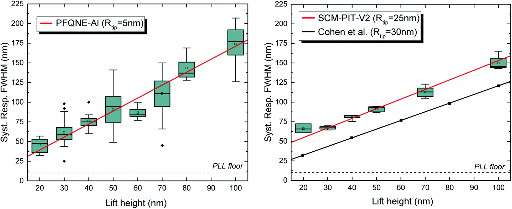 | ||
| Fig. 6 Measurements of the system impulse response performed using a calibration device with a gap length of 12 nm using Bruker PFQNE-Al tips (left) and Bruker SCM-PIT-V2 tips (right). The PLL floor is due to the numerical phase feedback loop. Simulations fromref. 21 are shown for comparison on the SCM-PIT-V2 graph (black plain line). | ||
Examples of a measured and a fitted potential profile are shown in Fig. 5. The theoretical potential profile (red lines in Fig. 5) was calculated by the convolution of a potential step Vsurf(x) of 1 V (dashed black line) with a Gaussian function g(x) (dashed green line), according to eqn (2). The Gaussian function g(x) represents the impulse response of the system for a given lift height and tip condition. The theoretical response is adjusted to match the measured profile, the fitting parameter being the FWHM of the Gaussian. No data processing of the measured potential profile was performed.
In this process, we do not intend to reconstruct the surface potential from the measured surface potential, as described in ref. 21 and 22. The proposed approach is based on an experimental determination of the system impulse response g(x) in a configuration as close as possible to that used while measuring the active devices of interest, namely thin-film transistors. The system impulse response g(x), including the tip PSF and other contributions such as the external phase feedback loop algorithm and related delays, is unknown and not the result of an electrostatic model, but rather approximated to a standard Gaussian function. The potential profile of the device under study Vsurf(x) is modeled as a simple potential step, and the experimental profile Vmeas(x) is fitted using this model convoluted by the system impulse response g(x). When calibrating the setup, the calibration sample potential profile Vsurf(x) is known and the system impulse response g(x) is estimated. When measuring a device, the system impulse response g(x) is known and the device potential profile Vsurf(x) is determined.
Using the proposed method and setup, a practical evaluation of the lateral resolution of the double-pass KPFM experiment was established, in conditions close to those used for the characterization of thin-film transistors. As discussed in the following section, this procedure was then used to compare the KPFM resolutions using different AFM tips and different lift heights, before applying the method to the study of organic thin-film transistors.
Results and discussion
Resolution measurements were performed using two types of conductive tips from Bruker: SCM-PIT-V2, with a typical radius of about 25 nm, and PFQNE-AL, with a typical radius of 5 nm. The oscillation amplitudes of both types of tips have been estimated from force-curve measurements. Using an amplitude setpoint of 120 mV, oscillation amplitudes of 4 to 4.5 nm and 3.5 to 5 nm have been estimated respectively for the SCMPIT-V2 and the PFQNE-AL tips respectively. The oscillation amplitudes of both tips remain small compared to the lift heights used in this work and are not expected to impact the resolution measurements.19,23 Except for the oscillation-amplitude measurements, the amplitude setpoint was adjusted for each individual experiment and varies typically from 90 mV to 130 mV.As mentioned, the measurements were performed on the calibration device with the smallest available gap length (12 nm). Resolution measurements were performed at several lift heights, and the resolution was extracted following the procedure described above. Fig. 6 shows the results of several tip-resolution measurements plotted versus the lift height for the SCM-PIT-V2 tips (black squares) and the PFQNE-AL tips (red circles).
Regardless of the choice of the tip (PFQNE-AL, SCM-PIT-V2), the measurement resolution degrades with increasing the lift height, as expected from an electrostatic point of view.19 The PFQNE-AL tips provide better resolution than the SCMPIT-V2 tips, as expected from the difference in tip radius (5 nm for the PFQNE-AL tips; 25 nm for the SCMPIT-V2 tips). From this figure it appears that the resolution of the present KPFM experiment increases linearly with the lift height for both tips, with reasonable confidence in the lift range considered. The slopes are (1.49 ± 0.07) nm nm−1 and (1.10 ± 0.05) nm nm−1 for the PFQNE-AL and SCMPIT-V2 probes, respectively. The intercept at zero lift height is (15.6 ± 3.4) nm for the PFQNE-AL tip and (37.2 ± 2.7) nm for the SCM-PIT-V2 tip. Taking into account the degradation of the resolution by 11 nm due to the phase feedback loop (determined from simulations of the feedback algorithm, as shown in Fig. 7), the zero lift height intercepts appear very close to the radius of the tips, at 5 nm and 25 nm for the PFQNE-AL and the SCM-PIT-V2 tips, respectively. Finally, this linear degradation of the resolution with lift height is in agreement with the simulations performed on similar systems: in ref. 21 a slope close to 1.0 nm nm−1 is found as shown Fig. 6 (right), while in ref. 19 slopes of 1.16 to 1.18 nm nm−1 are calculated for tip radii of 5 nm and 20 nm when the lift height is above the tip radius. The experimental resolution degradation rate with lift height is slightly above the simulation prediction for the PFQNE-AL tips. It remains important from an experimental point of view to work as close as possible to the surface.
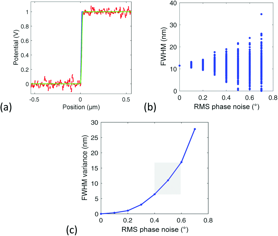 | ||
| Fig. 7 Simulation of the resolution dispersion induced by the phase feedback loop and phase noise. (a) Simulated potential profile (dashed red line) and fitted theoretical response (green solid line), showing the impact of random phase noise with a value of 2° on an ideal (perfectly abrupt) potential profile (black solid line). (b) Tip response FWHM extracted from 100 noisy potential profiles with random noise, simulated at each average value of the RMS phase noise, showing the dispersion of the determined FWHM. (c) Dependence of the variance of the tip FWHM on the RMS phase noise, extracted from the simulated data. The simulation algorithm performs exactly the same feedback process as the feedback loop implemented in the KPFM experiment. The grey area represents the actual KPFM setup RMS phase noise. | ||
As can be seen in Fig. 6, in particular for the PFQNE-AL probes, the measured system lateral resolutions show some degree of day-to-day and tip-to-tip variation, with a certain sensitivity to the experimental noise. In order to ensure an accurate determination of the system resolution, it appeared necessary to understand this behavior. The effect on the measured potential profiles of the phase feedback algorithm was simulated, including the various experimental measurement delays of the phase, and adding variable noise RMS amplitudes on the measured phases. This simulates the KPFM experiment response to a model potential profile. Various RMS noise levels were considered, and a theoretical (i.e., perfectly abrupt) potential step was considered (potential step of 1 V, electrode gap of zero). An example of a simulated profile is shown Fig. 7(a) (dashed red line). From the simulated noisy potential profile, an apparent tip response FWHM is determined by fitting the data with a Gaussian tip response, following eqn (2). The theoretical step profile and the corresponding fitted response are shown Fig. 7(a); the blue solid line is the theoretical step profile, and the green solid line is the best fit considering a Gaussian tip response with adjusted FWHM. Repeated simulations with random RMS phase noise were performed to evaluate the dispersion of the FWHM, as shown Fig. 7(b). First, due to the feedback-loop delay only, a FWHM floor of about 11 nm is observed. When adding phase noise, a significant FWHM variance appears. The variance reaches a value of 11 nm for an RMS phase noise of approximately 0.5°. This is the value of the phase noise typically observed in our experiment, which explains some of the dispersion observed in the resolution evaluation (Fig. 6). Three main conclusions are drawn: (i) the phase algorithm degrades the resolution by about 10 nm (ii) the variance of the measured system resolution is about 10 nm for the actual system phase noise, (iii) because of the dispersion induced by noise, several potential profiles must be measured to reduce the measurement uncertainty. Repeated line scans are important for an accurate determination of the resolution. Also, this simulation motivates more efforts to reduce noise in KPFM measurements.
Finally, at a lift height of 20 nm, which is the practical lower limit for the double-pass experiment performed here, the best reproducible resolution is about 40 nm for the PFQNE-Al tip and 60 nm for the SCM-PIT-tip. These resolutions are convenient for many applications, such as the characterization of thin-film transistors, as will be discussed below.
Application to organic thin-film transistors
The setup and resolution measurement technique presented above make it possible to accurately determine the potential profiles of organic thin-film transistors. Organic transistors usually have channel lengths on the order of 1 μm.24 We fabricated organic thin-film transistors in which the source and drain contacts were patterned either by stencil lithography,25 which produces relatively smooth contact edges,26 or by a combination of electron-beam lithography and lift-off,27 which produces very sharp contact edges. Both types of transistor were fabricated in the inverted coplanar (bottom-gate, bottom-contact) device architecture on heavily doped silicon substrates (serving as a global gate electrode) with a 10 nm-thick gate dielectric28 and using the vacuum-deposited small-molecule semiconductor dinaphtho[2,3-b:2′,3′-f]thieno[3,2-b]thiophene (DNTT)29 for the active layer. The nominal channel length of the transistors investigated here is 6 μm (stencil lithography) and 1.8 μm (electron-beam lithography). In both types of transistor, the surface of the aluminum oxide gate dielectric was functionalized with an n-tetradecylphosphonic acid self-assembled monolayer, and that of the gold source and drain contacts with a pentafluorobenzenethiol monolayer.25,27 These surface treatments induce a favorable thin-film morphology of the vacuum-deposited organic semiconductor DNTT, both on the gate-dielectric surface and on the surface of the source and drain contacts.The surface topography of the organic-semiconductor layer was measured by AFM near the edge of the source contact, both in the DNTT transistors fabricated by stencil lithography and in the ones fabricated by electron-beam lithography, as well as in the middle of the channel. The AFM images are shown in Fig. 8. The surface topography of vacuum-deposited DNTT films is usually characterized by the presence of tall features with a height of up to 100 nm,29 significantly above the nominal film thickness of 30 nm. The large density of these tall features makes it difficult to identify locations where the lift height can be safely reduced along the entire channel length. The lift height was thus adjusted to 80 nm for the stencil-patterned contact and 50 nm for the electron-beam-patterned contact. The larger lift height for the stencil-patterned contact was necessary, since the DNTT-topography profile near the stencil-patterned contacts indicated features with a height of almost 100 nm.
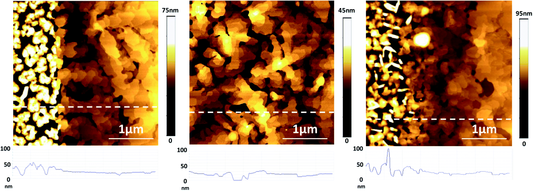 | ||
| Fig. 8 AFM topography of vacuum-deposited thin-films of the small-molecule organic semiconductor DNTT at the edge of a contact patterned by electron-beam lithography and lift-off (left), in the middle of the transistor channel (center), and at the edge of a contact patterned by stencil lithography (right). | ||
How sharp the contact edges of the transistors are is expected to have an impact on the surface potential profile and on the current–voltage characteristics of the transistors. A typical example of the surface potential profile measured across the contact edge of a DNTT transistor with source and drain contacts fabricated by stencil lithography is shown in Fig. 9.
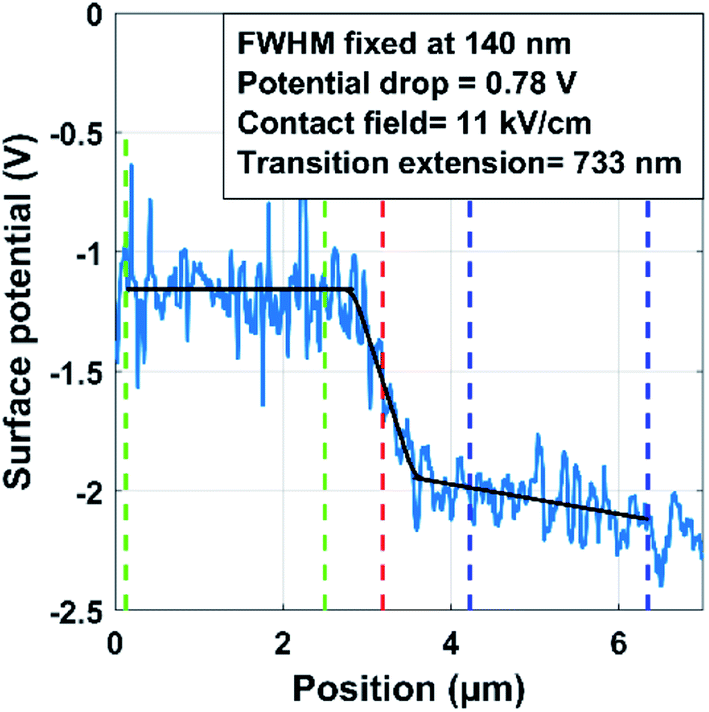 | ||
| Fig. 9 Surface potential profile measured at the interface between the source contact and the semiconductor channel of an organic thin-film transistor fabricated by stencil lithography (blue solid line), and fit to the potential profile using a tip response FWHM of 140 nm (black solid line). The fit parameters (contact potential drop, electric field, transition extension) are indicated. Channel length of the transistor: 6 μm. AFM tip: Bruker PFQNE-Al. Lift height: 80 nm. Drain-source voltage (UDS): −2.5 V. Gate-source voltage (UGS): −3.0 V. | ||
The impulse response was evaluated before and after the KPFM measurement in order to ensure stable resolution of the setup and be able to continuously monitor the tip condition. For a lift height of 30 nm, the FWHM of the impulse response was found to be virtually identical (57 nm before and 55 nm after the KPFM measurements), confirming a stable tip shape and stable measurement resolution.
To account for the smooth potential evolution observed in the transistors fabricated by stencil lithography, the potential profile at the contact edge was approximated as a linear slope between the source contact and the semiconductor channel, extending over a distance to be determined. Given the measurement conditions, the tip FWHM for a lift height of 80 nm was estimated to 140 nm. The measured surface potential profile was then fitted, as shown in Fig. 9 (black solid line). The potential drop extends over a lateral distance of approximately 730 nm, with a total drop of 0.78 V and an average electric field of only 11 kV cm−1. The electric field estimate is accurate in this case, since the lateral extension of the metal–semiconductor transition region is much larger than the KPFM experiment FWHM. The smooth contact edge appears to favor a smooth potential drop and thus a low injection field at the interface between the contact and the semiconductor channel. This was also observed by Ye et al.,30 who concluded that smooth contact edges allow for a favorable semiconductor morphology at the contact-channel interface.
Patterning the source and drain contacts by a combination of electron-beam lithography and lift-off, rather than stencil lithography, produces much sharper contact edges. The measured topography maps, 2D and 3D potential maps, and maps of the second derivative of the capacitance measured on a DNTT transistor with source and drain contacts fabricated by electron-beam lithography are shown in Fig. 10.
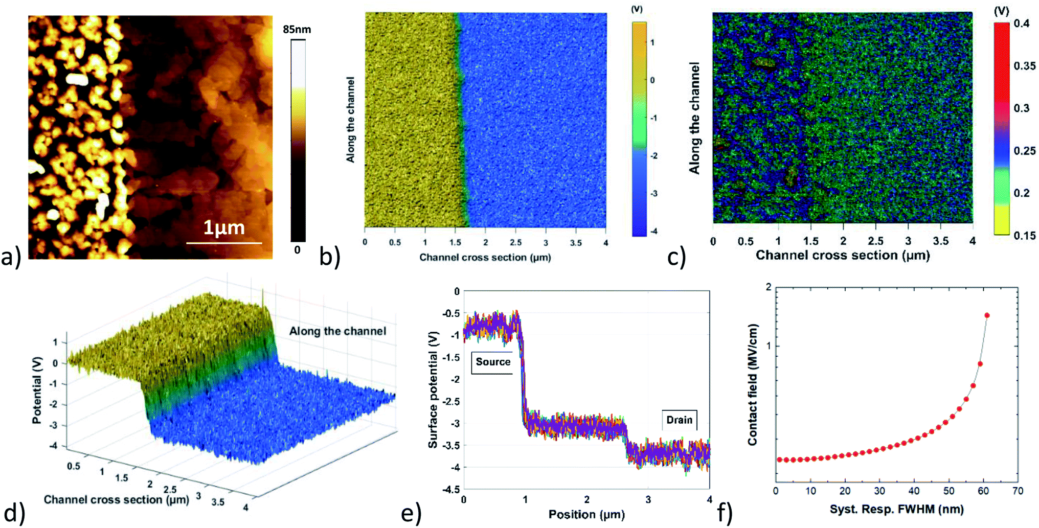 | ||
| Fig. 10 KPFM characterizations of the source contact of an organic thin-film transistor fabricated by a combination of electron-beam lithography and lift-off (a) topography map. (b) Surface potential map. (c) Map of the second derivative of the capacitance. (d) 3D potential map at the source-contact edge. (e) Potential profiles along the channel. (f) Contact field calculated as a function of the PSF FWHM. Channel length of the transistor: 1.8 μm. AFM tip: Bruker PFQNE-Al. Lift height: 50 nm. Drain-source voltage (UDS): −3 V. Gate-source voltage (UGS): −3 V. | ||
The surface-potential profiles in the transistors fabricated by electron-beam lithography are very different from those in the transistors fabricated by stencil lithography. A large and very steep potential drop is observed at the source contact edge over the entire channel width of the transistors fabricated by electron-beam lithography (Fig. 10(d)). The surface potential is constant over the Au source contact, and the voltage drop across the channel is only 0.1 V, while the potential drop at the edge of the source contact is 2.2 V. The conductivity is high both on the Au source contact and in the DNTT channel, compared to the low conductivity at the contact edge, which is responsible for the large potential drop. Also, the potential profile in the channel does not show any fluctuations, indicating a homogenous current flow and a homogeneous channel conductivity. As extracted from Fig. 4(d), the position of the potential drop follows the metallic source contact edge with very little fluctuations, showing a dispersion of only 50 nm from a straight-line approximation. Considering the large DNTT grain size observed in the AFM topography images (which sometimes exceeds 1 μm towards the channel; see Fig. 8(a)), it can be stated that the charges are not injected into the channel through these large grains, despite the observation that they sometimes overlap with the top of the Au contact. The potential profiles at the contacts fabricated by electron-beam lithography seem to indicate that the drain-current flow is limited mostly by an injection process occurring only at the edge of the sharp contact. The large and steep potential drop observed here is possibly the result of contamination from the electron-beam-lithography process, but it is more likely a direct consequence of the very sharp edges of the contacts when these are patterned by electron-beam lithography and lift-off, rather than stencil lithography. The influence of the sharpness of the edges of the source and drain contacts of DNTT transistors fabricated by stencil lithography on the surface-potential profile across the contact edges, on the DNTT morphology near the contact edges and on the contact resistance of the transistors was discussed by Ye et al.30
Assuming a perfectly abrupt contact edge, the raw measurement resolution extracted from 10 measured transistor potential profiles is FWHM = 64 nm, with a potential drop of 2.20 V, and the electric field is 260 kV cm−1. The experimental resolution for the optimum conditions (AFM tip: PFQNE-Al, lift height: 50 nm) is around 50 to 55 nm, i.e., very similar to the resolution obtained under the assumption of a perfect step edge, indicating a very sharp contact edge and a very sharp potential profile for the transistors fabricated by electron-beam lithography.
Taking into account the experimental resolution (FWHM = 50–55 nm), the injection electric field at the contact edge of the transistor fabricated by electron-beam lithography is estimated to range from 420 kV cm−1 to 540 kV cm−1, about 50 times higher than the electric field of the contacts with the smooth edges patterned by stencil lithography. Since these values are very sensitive to the resolution evaluation, a simulation of the extracted electric field was performed based on the measured surface potential profiles (Fig. 10(e)) and variable experimental resolution. Results are shown in Fig. 10(f). As mentioned, the minimum injection electric field is 260 kV cm−1 and increases rapidly beyond 500 kV cm−1 when a KPFM resolution above 55 nm is considered.
Considering the resolution measurement and uncertainties, the electric field at the contact edge of the transistor fabricated by electron-beam lithography is estimated to exceed 420 kV cm−1 and probably reaches 500 kV cm−1. This very high injection field indicates a low charge-injection efficiency from the source contact into the organic semiconductor. Such a high electric field is required if the charges must overcome a large injection barrier.31,32 The sharp contact edges in the transistor fabricated by electron-beam lithography appears to generate such a barrier.
Finally, thanks to the lateral resolution evaluation process implemented here, the present KPFM method appears well suited to analyze various contact technologies and to evaluate the injection field in thin-film transistors, measured from 10 kV cm−1 in the case of contacts patterned by stencil lithography, to more than 400 kV cm−1 in the case of contacts patterned by electron-beam lithography. This is believed to be a relevant contribution to the understanding of thin-film transistors and of the impact of the fabrication process, providing quantitative measurements of the contact potential drops and injection fields.
Conclusions
Targeting the reliable characterization of active electronic devices by KPFM, a double-pass method was used, based on a numerical feedback loop and lift mode. Since the lateral resolution of the surface electrical potential measurement is degraded by the tip-to-surface distance in lift mode, a method for estimating the lateral resolution of the present setup was developed. It uses a specially designed calibration sample with a nanometer gap between two conductive electrodes, achieving an abrupt potential step of 1 V. The system resolution was defined as the FWHM of the measured system impulse response on this quasi-planar surface. The method was successfully demonstrated to measure the resolution of different commercial AFM tips. At best, a lateral resolution of 40 nm was demonstrated in ambient conditions with a 20 nm lift height. The method can be used to monitor in situ the degradation of the tip. This is of particular interest for long KPFM measurement campaigns on active devices.Based on the knowledge of the tip response FWHM, quantitative exploitation of measured surface potential profiles becomes possible. Using this experiment, a study of the impact of the contact fabrication technology of organic thin-film transistors was conducted. Transistors with smooth and with sharp contacts were fabricated using stencil lithography and electron-beam lithography, respectively. The contact potential profiles close to the source contact edges were measured and compared. The electric field at the contact edges is reduced from more than 400 kV cm−1 to about 10 kV cm−1 respectively between the sharp and the smooth contacts. This difference has many impacts on the device performances and reliability. The capability to estimate the electric field responsible for the charge injection process at the metal/organic semiconductor interface is very important for modeling the device behavior. This is to our knowledge the first time such a measurement has been performed. The calibrated KPFM setup presented here is expected to help improve the knowledge of many electronic devices.
Conflicts of interest
There are no conflicts to declare.Acknowledgements
The authors thank the Region Champagne-Ardenne, URCA, DRRT Grand Est and FEDER program. The AFM experiments were performed in the NanoMat facility. The authors thank Grégoire De Tournadre for his contribution to the implementation of the KPFM experiment.References
- G. de Tournadre, F. Reisdorffer, R. Rödel, O. Simonetti, H. Klauk and L. Giraudet, High voltage surface potential measurements in ambient conditions: application to organic thin-film transistor injection and transport characterization, J. Appl. Phys., 2016, 119(12), 125501, DOI:10.1063/1.4944884.
- C. Riedel, et al., Determination of the nanoscale dielectric constant by means of a double pass method using electrostatic force microscopy, J. Appl. Phys., 2009, 106(2), 024315, DOI:10.1063/1.3182726.
- N. B. Bercu, L. Giraudet, O. Simonetti and M. Molinari, Development of an improved Kelvin probe force microscope for accurate local potential measurements on biased electronic devices, J. Microsc., 2017, 267(3), 272–279, DOI:10.1111/jmi.12563.
- D. Sarid, Scanning Force Microscopy, Oxford University Press, New York, 1994 Search PubMed.
- S. Gómez-Moñivas, L. S. Froufe, R. Carminati, J. J. Greffet and J. J. Sáenz, Tip-shape effects on electrostatic force microscopy resolution, Nanotechnology, 2001, 12(4), 496–499, DOI:10.1088/0957-4484/12/4/323.
- U. Zerweck, C. Loppacher, T. Otto, S. Grafström and L. M. Eng, Accuracy and resolution limits of Kelvin probe force microscopy, Phys. Rev. B: Condens. Matter Mater. Phys., 2005, 71(12), 125424, DOI:10.1103/PhysRevB.71.125424.
- P. Girard, Electrostatic force microscopy: principles and some applications to semiconductors, Nanotechnology, 2001, 12(4), 485–490, DOI:10.1088/0957-4484/12/4/321.
- J. Colchero, A. Gil and A. M. Baró, Resolution enhancement and improved data interpretation in electrostatic force microscopy, Phys. Rev. B: Condens. Matter Mater. Phys., 2001, 64(24), 245403, DOI:10.1103/PhysRevB.64.245403.
- S. Gómez-Moñivas, J. J. Sáenz, R. Carminati and J. J. Greffet, Theory of electrostatic probe microscopy: a simple perturbative approach, Appl. Phys. Lett., 2000, 76(20), 2955–2957, DOI:10.1063/1.126528.
- G. Li, B. Mao, F. Lan and L. Liu, Practical aspects of single-pass scan Kelvin probe force microscopy, Rev. Sci. Instrum., 2012, 83(11), 113701, DOI:10.1063/1.4761922.
- U. Zerweck, C. Loppacher, T. Otto, S. Grafström and L. M. Eng, Kelvin probe force microscopy of C60 on metal substrates: towards molecular resolution, Nanotechnology, 2007, 18(8), 084006, DOI:10.1088/0957-4484/18/8/084006.
- O. Douhéret, et al., High-resolution morphological and electrical characterisation of organic bulk heterojunction solar cells by scanning probe microscopy, Prog. Photovolt.: Res. Appl., 2007, 15(8), 713–726, DOI:10.1002/pip.795.
- J. L. Garrett and J. N. Munday, Fast, high-resolution surface potential measurements in air with heterodyne Kelvin probe force microscopy, Nanotechnology, 2016, 27(24), 245705, DOI:10.1088/0957-4484/27/24/245705.
- F. Krok, K. Sajewicz, J. Konior, M. Goryl, P. Piatkowski and M. Szymonski, Lateral resolution and potential sensitivity in Kelvin probe force microscopy: towards understanding of the sub-nanometer resolution, Phys. Rev. B: Condens. Matter Mater. Phys., 2008, 77(23), 235427, DOI:10.1103/PhysRevB.77.235427.
- D. C. Coffey and D. S. Ginger, Time-resolved electrostatic force microscopy of polymer solar cells, Nat. Mater., 2006, 5(9), 9, DOI:10.1038/nmat1712.
- Y. Chen, Nanofabrication by electron beam lithography and its applications: a review, Microelectron. Eng., 2015, 135, 57–72, DOI:10.1016/j.mee.2015.02.042.
- V. Panchal, et al., Standardization of surface potential measurements of graphene domains, Sci. Rep., 2013, 3, 2597, DOI:10.1038/srep02597.
- S. Belaidi, et al., Electrostatic forces acting on the tip in atomic force microscopy: modelization and comparison with analytic expression, J. Appl. Phys., 1997, 81(3), 1023–1030, DOI:10.1063/1.363884.
- G. Li, B. Mao, F. Lan and L. Liu, Practical aspects of single-pass scan Kelvin probe force microscopy, Rev. Sci. Instrum., 2012, 83, 113701, DOI:10.1063/1.4761922.
- H. O. Jacobs, P. Leuchtmann, O. J. Homan and A. Stemmer, Resolution and contrast in Kelvin probe force microscopy, J. Appl. Phys., 1998, 84(3), 1168–1173, DOI:10.1063/1.368181.
- G. Cohen, et al., Reconstruction of surface potential from Kelvin probe force microscopy images, Nanotechnology, 2013, 24(29), 295702, DOI:10.1088/0957-4484/24/29/295702.
- T. Machleidt, E. Sparrer, T. Kubertschak, R. Nestler and K. Franke, Kelvin Probe Force Microscopy: Measurement Data Reconstruction, Proc. SPIE, 2009, 7378, 737881C, DOI:10.1117/12.821787.
- F. J. Giessilb, Forces and frequency shifts in atomic-resolution dynamic-force microscopy, Phys. Rev. B: Condens. Matter Mater. Phys., 1997, 56, 24, DOI:10.1103/PhysRevB.56.16010.
- S. Elsaegh, et al., Low-Power Organic Light Sensor Array Based on Active-Matrix Common-Gate Transimpedance Amplifier on Foil for Imaging Applications, IEEE J. Solid-State Circuits, 2020, 55(9), 2553–2566, DOI:10.1109/JSSC.2020.2993732.
- J. W. Borchert, et al., Flexible low-voltage high-frequency organic thin-film transistors, Sci. Adv., 2020, 6(21), eaaz5156, DOI:10.1126/sciadv.aaz5156.
- O. Vazquez-Mena, L. G. Villanueva, V. Savu, K. Sidler, P. Langlet and J. Brugger, Analysis of the blurring in stencil lithography, Nanotechnology, 2009, 20(41), 415303, DOI:10.1088/0957-4484/20/41/415303.
- U. Zschieschang, et al., Roadmap to Gigahertz Organic Transistors, Adv. Funct. Mater., 2020, 30(20), 1903812, DOI:10.1002/adfm.201903812.
- M. Aghamohammadi, et al., Threshold-Voltage Shifts in Organic Transistors Due to Self-Assembled Monolayers at the Dielectric: Evidence for Electronic Coupling and Dipolar Effects, ACS Appl. Mater. Interfaces, 2015, 7(41), 22775–22785, DOI:10.1021/acsami.5b02747.
- U. Kraft, et al., Detailed analysis and contact properties of low-voltage organic thin-film transistors based on dinaphtho[2,3-b:2′,3′-f]thieno[3,2-b]thiophene (DNTT) and its didecyl and diphenyl derivatives, Org. Electron., 2016, 35, 33–40, DOI:10.1016/j.orgel.2016.04.038.
- X. Ye, et al., Blurred Electrode for Low Contact Resistance in Coplanar Organic Transistors, ACS Nano, 2021, 15(1), 1155–1166, DOI:10.1021/acsnano.0c08122.
- J. C. Scott and G. G. Malliaras, Charge injection and recombination at the metal–organic interface, Chem. Phys. Lett., 1999, 299(2), 115–119, DOI:10.1016/S0009-2614(98)01277-9.
- L. Giraudet and O. Simonetti, Threshold voltage and turn-on voltage in organic transistors: sensitivity to contact parasitics, Org. Electron., 2011, 12(1), 219–225, DOI:10.1016/j.orgel.2010.11.002.
Footnote |
| † Both authors contributed equally to this work. |
| This journal is © The Royal Society of Chemistry 2022 |