
 Open Access Article
 This Open Access Article is licensed under a
 Creative Commons Attribution 3.0 Unported Licence
Reconfigurable carrier type and photodetection of MoTe2 of various thicknesses by deep ultraviolet light illumination†
Byung Min
Ko‡
a,
Muhammad Farooq
Khan‡
 b,
Ghulam
Dastgeer
a,
Gyu Nam
Han
a,
Muhammad Asghar
Khan
a and
Jonghwa
Eom
*a
b,
Ghulam
Dastgeer
a,
Gyu Nam
Han
a,
Muhammad Asghar
Khan
a and
Jonghwa
Eom
*a
aDepartment of Physics & Astronomy and Graphene Research Institute, Sejong University, Seoul 05006, Korea. E-mail: eom@sejong.ac.kr
bDepartment of Electrical Engineering, Sejong University, 209 Neungdong-ro, Gwangjin-gu, Seoul 05006, Korea
First published on 10th May 2022
Abstract
Tuning of the Fermi level in transition metal dichalcogenides (TMDCs) leads to devices with excellent electrical and optical properties. In this study, we controlled the Fermi level of MoTe2 by deep ultraviolet (DUV) light illumination in different gaseous environments. Specifically, we investigated the reconfigurable carrier type of an intrinsic p-MoTe2 flake that gradually transformed into n-MoTe2 after illumination with DUV light for 30, 60, 90, 120, 160, 250, 500, 900, and 1200 s in a nitrogen (N2) gas environment. Subsequently, we illuminated this n-MoTe2 sample with DUV light in oxygen (O2) gas and reversed its carrier polarity toward p-MoTe2. However, using this doping scheme to reveal the effect of DUV light on various layers (3–30 nm) of MoTe2 is challenging. The DUV + N2 treatment significantly altered the polarity of MoTe2 of different thicknesses from p-type to n-type under the DUV + N2 treatment, but the DUV + O2 treatment did not completely alter the polarity of thicker n-MoTe2 flakes to p-type. In addition, we investigated the photoresponse of MoTe2 after DUV light treatment in N2 and O2 gas environments. From the time-resolved photoresponsivity at different polarity states of MoTe2, we have shown that the response time of the DUV + O2 treated p-MoTe2 is faster than that of the pristine and doped n-MoTe2 films. These carrier polarity modulations and photoresponse paves the way for wider applications of MoTe2 in optoelectronic devices.
Introduction
Recently, two-dimensional (2D) nanomaterials have gained significant attention because of their unique optical and electrical properties.1–3 Graphene has been the focus of modern research in the past few years because of its high intrinsic electron mobility of 200![[thin space (1/6-em)]](https://www.rsc.org/images/entities/char_2009.gif) 000 cm2 V s−1 and high thermal conductivity of approximately 4400 to 5780 W m K−1 at room temperature.4,5 In addition, the transmittance of light was found to be 97.7% at 550 nm owing to the small thickness of a single layer.6 However, the absence of the bandgap in graphene initiates the search for other 2D bandgap materials, which is necessary for switching device applications. Transition metal dichalcogenides (TMDCs) have a significant bandgap range of approximately 1.0 to 2.5 eV, which facilitates fabrication of atomically thin p–n diodes such as MoTe2/MoS2, WSe2/MoS2 and black phosphorus/IGZO.7–9 The Fermi level of TMDCs is near the center between conduction and valence bands,10 but most TMDCs used in experiments are naturally n-type or p-type doped due to intrinsic structural defects and interface impurities.11,12
000 cm2 V s−1 and high thermal conductivity of approximately 4400 to 5780 W m K−1 at room temperature.4,5 In addition, the transmittance of light was found to be 97.7% at 550 nm owing to the small thickness of a single layer.6 However, the absence of the bandgap in graphene initiates the search for other 2D bandgap materials, which is necessary for switching device applications. Transition metal dichalcogenides (TMDCs) have a significant bandgap range of approximately 1.0 to 2.5 eV, which facilitates fabrication of atomically thin p–n diodes such as MoTe2/MoS2, WSe2/MoS2 and black phosphorus/IGZO.7–9 The Fermi level of TMDCs is near the center between conduction and valence bands,10 but most TMDCs used in experiments are naturally n-type or p-type doped due to intrinsic structural defects and interface impurities.11,12
Controlled modulation of the Fermi level in the bandgap of TMDCs has been exploited in various reports for device applications.13,14 While most of the well-known TMDCs such as WS2, MoS2, MoSe2, ReSe2, and ReS2 are observed to be n-type semiconductors, MoTe2 is p-type when thin, and shows ambipolar and n-type properties in thicker forms.15–19 In addition, MoTe2 has shown great potential in applications, such as chemical sensors, memristors, and photodetectors.20–22 The thicker hexagonal structure of MoTe2 has a bandgap of 0.88 eV, whereas its mono-layer exhibits a direct bandgap of almost 1.1 eV.23,24 The narrow bandgap also enables a huge tunneling current and a high on-off ratio of MoTe2 FETs. The pinning of the Fermi level at the MoTe2-metal interface is not as strong as that of sulfur-terminated TMDCs.25 Thus, the weak pinning and small bandgap of MoTe2 make the Fermi level modulation feasible and carrier polarity controllable by various techniques. The doping treatment of MoTe2 has been accomplished by electrostatic gating, chemical doping, and work function engineering with different metal electrodes; however, the doping effect was weak and too volatile for electronic devices.26–28 Designing a constructive approach that provides non-volatility and reversibility of charge carrier polarity in 2D TMDC materials is indispensable. Therefore, MoTe2 with layers of different thicknesses is a promising candidate for overcoming the abovementioned challenges. However, there is still ambiguity in the doping effect and carrier-type inversion of MoTe2 layers with different thicknesses when exposed to deep ultraviolet (DUV) light in various gaseous environments.
In this study, we fabricated a MoTe2 field-effect transistor (FET) on a SiO2 substrate using the mechanical exfoliation technique. We exposed MoTe2 thin-film FETs under deep ultraviolet (DUV) light for different illumination times in the presence of different gases (N2 or O2), which resulted in a non-volatile doping effect and inversion of charge carrier polarity in MoTe2 FETs. In addition, we investigated the photodetection of DUV light after a variety of doping treatments (pristine p-MoTe2, DUV + N2 treatment, and DUV + O2 treatment).
Fabrication
We fabricated a MoTe2 FET on a SiO2 substrate (Fig. 1a) to elucidate the carrier polarity modification. Bulk MoTe2 was first put on tape and then exfoliated to make the MoTe2 thin films.29 Then, the tape was pressed on top of polydimethylsiloxane (PDMS). Subsequently, PDMS was stamped on the desired area on the Si/SiO2 substrates.30 A MoTe2 thin film was produced as confirmed using optical microscopy. Then, conventional e-beam lithography was employed to make Cr/Au (5 nm/60 nm) electrical contacts, which were annealed at 100 °C for 1.5 h to improve the ohmic properties.30–32 The optical microscope images of the final device are shown in Fig. 1a. Meanwhile, the thickness of the flakes was investigated using atomic force microscopy (AFM). Fig. 1b and c show the AFM images of the film and the thickness of the exfoliated MoTe2 film was found to be approximately 6.5 nm.15,33 Then, the crystal properties of MoTe2 were examined by Raman spectroscopy15 as shown in Fig. 1d.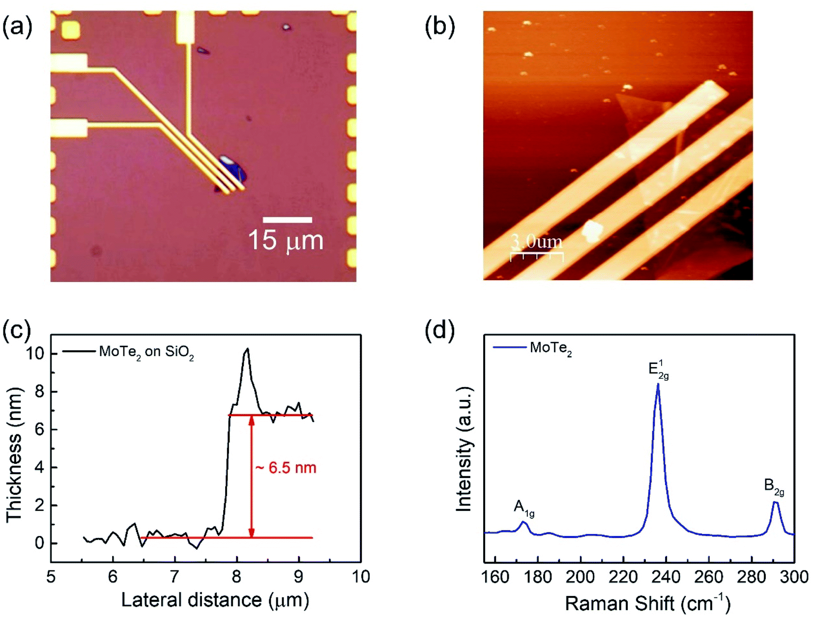 | ||
| Fig. 1 (a) Optical microscope image of the MoTe2 device. (b) Atomic force microscopy (AFM) image of the MoTe2 device. (c) The thickness profile of the MoTe2 thin film by AFM. (d) The Raman spectroscopy image of the MoTe2 film under ambient conditions. | ||
Furthermore, the DUV doping treatments were performed in N2 and O2 gas environments at a pressure of 0.8 bar. The average intensity of the DUV light was 11 mW cm−2, which was measured at a wavelength of 220 nm.
Results and discussion
Transition from intrinsic p-type MoTe2 to n-type MoTe2
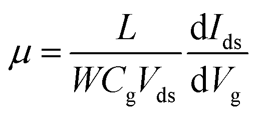
Raman spectroscopy was performed to examine the crystal bonding properties and estimate the thickness of the pristine MoTe2 flakes. Fig. 1d shows the Raman spectrum of MoTe2 obtained using a Renishaw microspectrometer with a laser wavelength of 514 nm and an optical intensity of 1 mW cm−2. Three vibrational modes were observed, namely, A1g, E2g1 and B2g1 at approximately 173.8 cm−1, 236.2 cm−1, and 291.1 cm−1, respectively. These results reveal five layers of MoTe2, which is almost consistent with previous reports.34,35Furthermore, we investigated the intrinsic nature of the charge carriers of the MoTe2 flakes by measuring the transfer curves (Idsvs. Vg) at a fixed source–drain bias voltage Vds = 1 V. After sweeping the gate voltage from −60 to 60 V, a threshold current (Ids) was observed in the negative gate voltage regime, confirming the p-type nature of the pristine MoTe2 flake, as shown in Fig. 2a. Subsequently, we treated the pristine p-MoTe2 with DUV light in a N2 environment (DUV + N2) for 1200 s to obtain n-MoTe2. The change in the charge carrier type was confirmed by using the Ids–Vg transfer curves, as shown in Fig. 2b. The DUV exposure time was varied from 0 to 1200 s, with a time interval of 30 s. The DUV + N2 treatment gave rise to n-type doping in MoTe2. The Fermi level of the intrinsic p-type MoTe2 was near the valence band, but after the DUV + N2 treatment, the Fermi level shifted near the conduction band. This Fermi level shift is responsible for the change in the nature of the MoTe2 flakes from p- to n-type. To verify the doping mechanism more precisely, the mobility of electrons/holes of intrinsic p-MoTe2 and n-MoTe2 (after DUV + N2 treatment) sheets was extracted from the transfer curves using the following equation:
 | (1) |
 | ||
| Fig. 2 (a) Transfer curve (Ids–Vg) of the intrinsic p-MoTe2 device. (b) The transfer curves at different DUV + N2 treatment times. (c) Electron and hole mobility at different DUV + N2 treatment times. (d) The charge carrier density of electrons and holes of the MoTe2 flake for various DUV + N2 treatment times. | ||
Moreover, the charge carrier density of holes in p-type MoTe2 and electrons in DUV + N2 treated MoTe2 sheets was calculated using the relation:37,38
| n = q−1Cg|Vth − Vg| | (2) |
Transition from n-type MoTe2 to p-type MoTe2
Interestingly, the n-MoTe2 flake, which was treated with DUV + N2 for 1200 s, could be reconfigured to p-MoTe2 by DUV + O2 treatment. As mentioned previously, the source–drain voltage was fixed at Vds = 1 V, and the back-gate voltage was applied to the substrate to check the Ids–Vg transfer curve from 60 V to −60 V. Fig. 3a shows the transfer curve of n-MoTe2 treated with DUV + N2 for 1200 s. Then, the transfer curves were measured as we increased the treatment time of DUV + O2, as shown in Fig. 3b. The mobility of the electrons (holes) in the n-MoTe2 sheets was estimated to be 0.25 cm2 V−1 s−1 (3.8 cm2 V−1 s−1) after the DUV + O2 treatment, as shown in Fig. 3c. As the exposure time of the DUV + O2 treatment increased from 0 to 1200 s, the mobility of electrons decreased, while the mobility of holes increased. Similarly, the carrier density of the holes (electrons) at a fixed gate voltage of ±40 V increased (decreased) with increasing exposure time, as shown in Fig. 3d. Initially, the carrier density increased abruptly but started to saturate with time after 200 s. The increase in the hole density indicates that the nature of n-type MoTe2 shifted back to that of p-type MoTe2 after the DUV + O2 treatment. This reverse doping could be ascribed to the oxygen donor molecules under DUV light, and the shift of the MoTe2 Fermi level near the valence band. In case of transition from pristine p-MoTe2 to n-MoTe2, the current and mobility values are saturated after 1200 s DUV + N2 treatment as shown in Fig. S2a and S2b (see the ESI†). On the other hand, when n-type doped MoTe2 (self-made) is converted to p-MoTe2 by DUV + O2 treatment, the current and mobility values reach the maximum values, but after 1200 s they slightly start to degrade due to weak oxidation of MoTe2 under DUV + O2 treatment (see Fig. S1c and S1d†).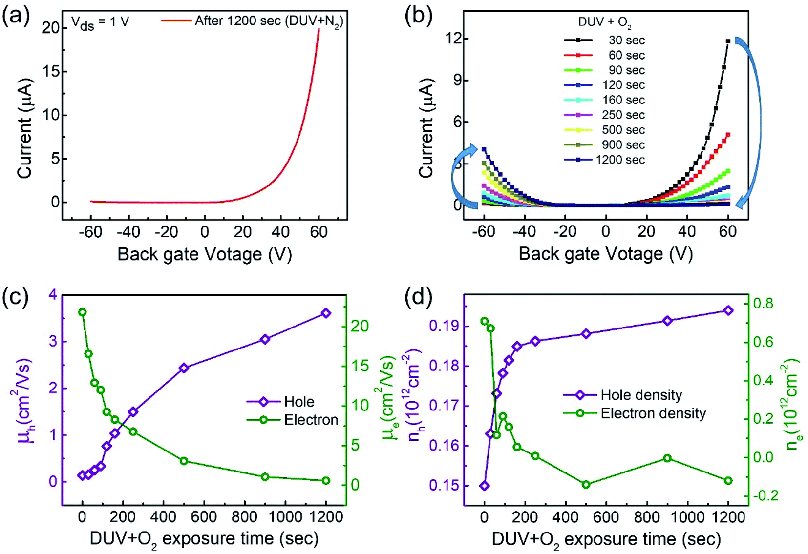 | ||
| Fig. 3 (a) Transfer curve of the MoTe2 device after DUV + N2 doping for 1200 s. (b) Transfer curves after DUV + O2 treatments for various times. (c) Electron and hole mobility for various DUV + O2 treatment times. (d) Charge carrier density of electrons and holes of the MoTe2 flake for various DUV + O2 treatment times. | ||
In addition, we investigated several intrinsic p-MoTe2 devices with different flake thickness values under DUV light in N2 and O2 environments. AFM images and thickness profiles of the devices are shown in Fig. S2.† As shown in Fig. 4a, we measured the Ids–Vg curves of intrinsic MoTe2 devices with different thicknesses (3.1, 5.9, 14, and 30 nm). However, we found that the thin flake devices showed only p-type behavior, whereas the thicker flakes showed ambipolar or n-type characteristics. After the DUV + N2 treatment, all devices were then completely configured into n-type, as shown in Fig. 4b. Subsequently, we exposed the n-MoTe2 devices to DUV + O2 treatment, which altered all the n-type devices to p-type. Interestingly, only the thin devices completely changed their polarities. The thicker devices did not completely change back to p-type but showed ambipolar behavior, as shown in Fig. 4c. The DUV + O2 treatment did not fully dope the thick flakes. Furthermore, the mobilities of electrons and holes for all devices (pristine, after DUV + N2, and DUV + O2 treatments) were estimated, as shown in Fig. 4d and e. While the 3.1 nm-thick MoTe2 flake was p-type in the pristine state, the 30 nm-thick MoTe2 flake was n-type in the pristine state. We found that the DUV treatments were more efficient for thinner MoTe2 flakes.
 | ||
| Fig. 4 Transfer curves of (a) pristine p-MoTe2 flakes. (b) DUV + N2 treated MoTe2 flakes. (c) DUV + O2 treated MoTe2 flakes. (d) Hole mobility of all devices having different thicknesses of MoTe2. (e) Electron mobility of all devices with different thicknesses of MoTe2. | ||
Photodetector measurements
The key factors in photodetection are current photo-generation and photoresponsivity, which play promising roles in optical devices. Therefore, the time-resolved photoresponse of the fabricated FETs was examined under a DUV lamp (λ = 220 nm, P = 11 mW cm−2) in a vacuum box. The newly fabricated device was first imaged as shown in Fig. 5a. For comparison, the response of the pristine p-MoTe2, n-MoTe2 after DUV + N2 treatment, and p-MoTe2 after DUV + O2 treatment under DUV light irradiation was observed in a vacuum at Vg = 0 V and Vds = 0.5 V. When the DUV light on the pristine p-MoTe2 photodetector was switched ON (for 60 s), a photocurrent was generated owing to electron–hole pair generation. Then, the photocurrent quickly dropped toward its initial state when the DUV light was switched OFF (for 60 s), as shown in Fig. 5b. The photoresponse of the pristine MoTe2 device is shown in Fig. 5b.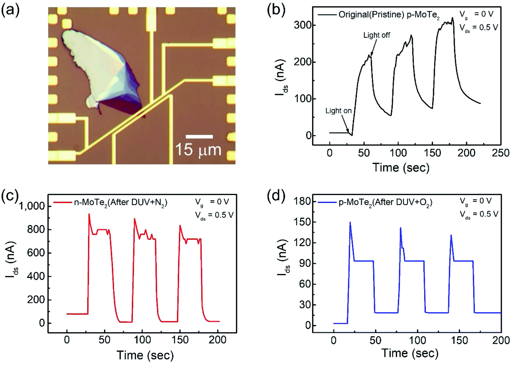 | ||
| Fig. 5 (a) Optical microscope image of the pristine p-MoTe2 device. Photoresponse of (b) pristine p-MoTe2, (c) after 1200 s DUV + N2 treatment and (d) after 1200 s DUV + O2 treatment. | ||
Meanwhile, the self-made n-MoTe2 photodetector after DUV + N2 doping showed a faster response with higher photocurrent values, as shown in Fig. 5c. This increase in the photocurrent is likely due to the large electron density caused by DUV + N2 doping, which facilitates the charge carrier transport after the generation of electron–hole pairs by DUV light. Furthermore, for the self-made p-MoTe2 device after DUV + O2 doping, the photoresponse is faster but the photocurrent magnitude is reduced, as shown in Fig. 5d. The reduced current is attributed to the oxygen trap states formed by DUV + O2. However, the sharp rise and decay of the n-MoTe2 and p-MoTe2 photodetectors (Fig. 5c and d) are expected to occur because of the additional energy states in MoTe2 (n- and p-type) with N2 and O2 treatment under DUV light. When the DUV light is turned ON, an abrupt rise in the photocurrent is produced due to electron–hole pair generation, but electrons are quickly captured in trapping states of the defects and the current quickly falls down to a saturation level.
To elucidate the photoresponse in detail, we calculated the photoresponsivity of each device (Fig. 6a). The responsivities of pristine MoTe2, DUV + N2 doped MoTe2 (n-MoTe2), and DUV + O2 doped MoTe2 (p-MoTe2) were found to be approximately 183, 1080, and 18 A/W, respectively. This trend is expected because the DUV + O2 treated p-MoTe2 device exhibited low photocurrent generation (approximately 12 nA) compared to pristine p-MoTe2 (110 nA) and DUV + N2 doped devices (713 nA), as shown in Fig. S3.† The lower photocurrent in the DUV + O2 treated devices can be ascribed to the quick recombination of photogenerated charges in defect states of p-type MoTe2.
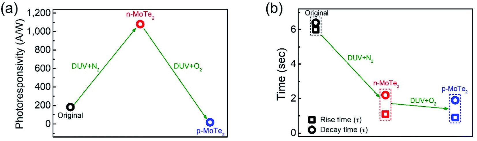 | ||
| Fig. 6 (a) Photoresponsivity of pristine p-MoTe2, DUV + N2 treated and DUV + O2 treated devices. (b) Response time (rise & decay) of MoTe2 photodetectors of each type. The rectangular shape represents the rise time constant and circle shape represents the decay time constant. | ||
The response times of the pristine MoTe2, DUV + N2 doped n-MoTe2, and DUV + O2 doped p-MoTe2 devices were also extracted after fitting the following equations:39,40
| It = Idark + A(1 − e−t/λ1) and It = Idark + Be−t/λ2 | (3) |
Conclusion
In summary, FETs were fabricated using pristine p-MoTe2, n-MoTe2 (after DUV + N2 treatment), and p-MoTe2 (after DUV + O2 treatment). The pristine p-MoTe2 gradually changed to n-MoTe2 after DUV + N2 treatment. Subsequently, the treated n-MoTe2 was reconfigured to p-MoTe2 by DUV + O2 treatment. We estimated that the field-effect mobility and charge carrier density of electrons/holes significantly changed under the DUV + N2/O2 treatments. In addition, we investigated each type of the MoTe2 photodetector at Vg = 0 V and found that the photocurrent of n-MoTe2 was higher than that of intrinsic p-MoTe2 and treated p-MoTe2. The DUV + O2 treated p-MoTe2 devices exhibited slightly poor performance owing to the O2 based electron trapping states in MoTe2. Interestingly, we found that the polarity of thin MoTe2 flakes could be easily changed from p-type to n-type and then from n-type to p-type, whereas the thicker MoTe2 flakes could easily transform into an n-type material after DUV + N2 treatment; however, their polarities were not entirely transformed from n-type to p-type after DUV + O2 treatment. Moreover, we found that the response time of DUV + O2 treated p-MoTe2 is faster than that of intrinsic p-MoTe2 and DUV + N2 treated n-MoTe2, which is attributed to the additional trapping/oxide states in the DUV + O2 treated p-MoTe2 flake. We believe that such a reversibility of carrier polarity by DUV + N2/O2 treatment can be utilized for the next generation of optoelectronic devices.Conflicts of interest
The authors declare no competing financial interests.Acknowledgements
This work was supported by grants No. 2021R1A4A1031900, the Basic Science Research Program (2019R1F1A1057697), and the Global Research and Development Center Program (2018K1A4A3A01064272) through a National Research Foundation of Korea (NRF) grant funded by the Korean government (Ministry of Education and the Ministry of Science and ICT).References
- Y. Yang, Z. Liu, K. Shu, L. Li and J. Li, Adv. Mater. Interfaces, 2021, 2100164 CrossRef CAS.
- X. Zhai, X. Xu, J. Peng, F. Jing, Q. Zhang, H. Liu and Z. Hu, ACS Appl. Mater. Interfaces, 2020, 12, 24093–24101 CrossRef CAS PubMed.
- S. Rehman, H. Kim, M. F. Khan, J.-H. Hur, J. Eom and D.-k. Kim, J. Alloys Compd., 2021, 855, 157310 CrossRef CAS.
- K. I. Bolotin, K. J. Sikes, Z. Jiang, M. Klima, G. Fudenberg, J. Hone, P. Kim and H. L. Stormer, Solid State Commun., 2008, 146, 351–355 CrossRef CAS.
- A. A. Balandin, S. Ghosh, W. Bao, I. Calizo, D. Teweldebrhan, F. Miao and C. N. Lau, Nano Lett., 2008, 8, 902–907 CrossRef CAS PubMed.
- S.-E. Zhu, S. Yuan and G. C. A. M. Janssen, Europhys. Lett., 2014, 108, 17007 CrossRef.
- A. Pezeshki, S. H. H. Shokouh, T. Nazari, K. Oh and S. Im, Adv. Mater., 2016, 28, 3216–3222 CrossRef CAS PubMed.
- R. Cheng, D. Li, H. Zhou, C. Wang, A. Yin, S. Jiang, Y. Liu, Y. Chen, Y. Huang and X. Duan, Nano Lett., 2014, 14, 5590–5597 CrossRef CAS PubMed.
- G. Dastgeer, M. F. Khan, J. Cha, A. M. Afzal, K. H. Min, B. M. Ko, H. Liu, S. Hong and J. Eom, ACS Appl. Mater. Interfaces, 2019, 11, 10959–10966 CrossRef CAS PubMed.
- C. Kittel, Introduction to Solid State Physics, Wiley, Sussex, Eng., United Kingdom, Fifth edition, 1976 Search PubMed.
- D. Rhodes, S. H. Chae, R. Ribeiro-Palau and J. Hone, Nat. Mater., 2019, 18, 541–549 CrossRef CAS PubMed.
- M. F. Khan, F. Ahmed, S. Rehman, I. Akhtar, M. A. Rehman, P. A. Shinde, K. Khan, D.-k. Kim, J. Eom and H. Lipsanen, Nanoscale, 2020, 12, 21280–21290 RSC.
- D.-H. Kang, J. Shim, S. K. Jang, J. Jeon, M. H. Jeon, G. Y. Yeom, W.-S. Jung, Y. H. Jang, S. Lee and J.-H. Park, ACS Nano, 2015, 9, 1099–1107 CrossRef CAS PubMed.
- S. Zhang, H. M. Hill, K. Moudgil, C. A. Richter, A. R. Hight Walker, S. Barlow, S. R. Marder, C. A. Hacker and S. J. Pookpanratana, Adv. Mater., 2018, 30, 1802991 CrossRef PubMed.
- C. Ruppert, O. B. Aslan and T. F. Heinz, Nano Lett., 2014, 14, 6231–6236 CrossRef CAS PubMed.
- A. Eftekhari, J. Mater. Chem. A, 2017, 5, 18299–18325 RSC.
- O. Lopez-Sanchez, D. Lembke, M. Kayci, A. Radenovic and A. Kis, Nat. Nanotechnol., 2013, 8, 497–501 CrossRef CAS PubMed.
- M. F. Khan, S. Rehman, I. Akhtar, S. Aftab, H. M. S. Ajmal, W. Khan, D.-k. Kim and J. Eom, 2D Materials, 2019, 7, 015010 CrossRef.
- E. Zhang, Y. Jin, X. Yuan, W. Wang, C. Zhang, L. Tang, S. Liu, P. Zhou, W. Hu and F. Xiu, Adv. Funct. Mater., 2015, 25, 4076–4082 CrossRef CAS.
- Z. Feng, Y. Xie, J. Chen, Y. Yu, S. Zheng, R. Zhang, Q. Li, X. Chen, C. Sun and H. Zhang, 2D Materials, 2017, 4, 025018 CrossRef.
- L. Sun, M. Ding, J. Li, L. Yang, X. Lou, Z. Xie, W. Zhang and H. Chang, Appl. Surf. Sci., 2019, 496, 143687 CrossRef CAS.
- H. Huang, J. Wang, W. Hu, L. Liao, P. Wang, X. Wang, F. Gong, Y. Chen, G. Wu and W. Luo, Nanotechnology, 2016, 27, 445201 CrossRef PubMed.
- D. H. Keum, S. Cho, J. H. Kim, D.-H. Choe, H.-J. Sung, M. Kan, H. Kang, J.-Y. Hwang, S. W. Kim and H. Yang, Nat. Phys., 2015, 11, 482–486 Search PubMed.
- J. S. Cho, H. S. Ju, J.-K. Lee and Y. C. Kang, Nanoscale, 2017, 9, 1942–1950 RSC.
- C. Kim, I. Moon, D. Lee, M. S. Choi, F. Ahmed, S. Nam, Y. Cho, H.-J. Shin, S. Park and W. J. Yoo, ACS Nano, 2017, 11, 1588–1596 CrossRef CAS PubMed.
- S. Larentis, B. Fallahazad, H. C. Movva, K. Kim, A. Rai, T. Taniguchi, K. Watanabe, S. K. Banerjee and E. Tutuc, ACS Nano, 2017, 11, 4832–4839 CrossRef CAS PubMed.
- W. Luo, M. Zhu, G. Peng, X. Zheng, F. Miao, S. Bai, X. A. Zhang and S. Qin, Adv. Funct. Mater., 2018, 28, 1704539 CrossRef.
- A. Pezeshki, S. H. Hosseini Shokouh, P. J. Jeon, I. Shackery, J. S. Kim, I.-K. Oh, S. C. Jun, H. Kim and S. Im, ACS Nano, 2016, 10, 1118–1125 CrossRef CAS PubMed.
- K. S. Novoselov, Angew. Chem., Int. Ed., 2011, 50, 6986–7002 CrossRef CAS PubMed.
- R. Yang, X. Zheng, Z. Wang, C. J. Miller and P. X. L. Feng, J. Vac. Sci. Technol., B: Nanotechnol. Microelectron.: Mater., Process., Meas., Phenom., 2014, 32, 061203 Search PubMed.
- J. Lin, S. T. Pantelides and W. Zhou, ACS Nano, 2015, 9, 5189–5197 CrossRef CAS PubMed.
- D. Qi, Q. Wang, C. Han, J. Jiang, Y. Zheng, W. Chen, W. Zhang and A. T. S. Wee, 2D Materials, 2017, 4, 045016 CrossRef.
- I. G. Lezama, A. Arora, A. Ubaldini, C. Barreteau, E. Giannini, M. Potemski and A. F. Morpurgo, Nano Lett., 2015, 15, 2336–2342 CrossRef CAS PubMed.
- M. Grzeszczyk, K. Gołasa, M. Zinkiewicz, K. Nogajewski, M. R. Molas, M. Potemski, A. Wysmołek and A. Babiński, 2D Materials, 2016, 3, 025010 CrossRef.
- M. Yamamoto, S. T. Wang, M. Ni, Y.-F. Lin, S.-L. Li, S. Aikawa, W.-B. Jian, K. Ueno, K. Wakabayashi and K. Tsukagoshi, ACS Nano, 2014, 8, 3895–3903 CrossRef CAS PubMed.
- M. W. Iqbal, M. Z. Iqbal, M. F. Khan, M. A. Shehzad, Y. Seo, J. H. Park, C. Hwang and J. Eom, Sci. Rep., 2015, 5, 10699 CrossRef CAS PubMed.
- Y.-H. Lee, L. Yu, H. Wang, W. Fang, X. Ling, Y. Shi, C.-T. Lin, J.-K. Huang, M.-T. Chang, C.-S. Chang, M. Dresselhaus, T. Palacios, L.-J. Li and J. Kong, Nano Lett., 2013, 13, 1852–1857 CrossRef CAS PubMed.
- J. D. Lin, C. Han, F. Wang, R. Wang, D. Xiang, S. Qin, X.-A. Zhang, L. Wang, H. Zhang, A. T. S. Wee and W. Chen, ACS Nano, 2014, 8, 5323–5329 CrossRef CAS PubMed.
- B. Chitara, S. B. Krupanidhi and C. N. R. Rao, Appl. Phys. Lett., 2011, 99, 113114 CrossRef.
- Y. Miyamoto, D. Yoshikawa, K. Takei, T. Arie and S. Akita, Jpn. J. Appl. Phys., 2018, 57, 06HB01 CrossRef.
Footnotes |
| † Electronic supplementary information (ESI) available. See https://doi.org/10.1039/d1na00881a |
| ‡ These authors contributed equally. |
| This journal is © The Royal Society of Chemistry 2022 |