
 Open Access Article
 This Open Access Article is licensed under a Creative Commons Attribution-Non Commercial 3.0 Unported Licence
A controlled nucleation and growth of Si nanowires by using a TiN diffusion barrier layer for lithium-ion batteries†
Dongheun
Kim
a,
Towfiq
Ahmed
 b,
Kenneth
Crossley
a,
J. Kevin
Baldwin
a,
Sun Hae
Ra Shin‡
a,
Yeonhoo
Kim§
a,
Chris
Sheehan
a,
Nan
Li
a,
Doug V.
Pete
c,
Henry H.
Han‡
*a and
Jinkyoung
Yoo
*a
b,
Kenneth
Crossley
a,
J. Kevin
Baldwin
a,
Sun Hae
Ra Shin‡
a,
Yeonhoo
Kim§
a,
Chris
Sheehan
a,
Nan
Li
a,
Doug V.
Pete
c,
Henry H.
Han‡
*a and
Jinkyoung
Yoo
*a
aCenter for Integrated Nanotechnologies, Los Alamos National Laboratory, Los Alamos, NM 87545, USA. E-mail: hhan@pnnl.gov; jyoo@lanl.gov
bT-4, Los Alamos National Laboratory, Los Alamos, NM 87545, USA
cCenter for Integrated Nanotechnologies, Sandia National Laboratories, Albuquerque, NM 87110, USA
First published on 9th March 2022
Abstract
Uniform size of Si nanowires (NWs) is highly desirable to enhance the performance of Si NW-based lithium-ion batteries. To achieve a narrow size distribution of Si NWs, the formation of bulk-like Si structures such as islands and chunks needs to be inhibited during nucleation and growth of Si NWs. We developed a simple approach to control the nucleation of Si NWs via interfacial energy tuning between metal catalysts and substrates by introducing a conductive diffusion barrier. Owing to the high interfacial energy between Au and TiN, agglomeration of Au nanoparticle catalysts was restrained on a TiN layer which induced the formation of small Au nanoparticle catalysts on TiN-coated substrates. The resulting Au catalysts led to the nucleation and growth of Si NWs on the TiN layer with higher number density and direct integration of the Si NWs onto current collectors without the formation of bulk-like Si structures. The lithium-ion battery anodes based on Si NWs grown on TiN-coated current collectors showed improved specific gravimetric capacities (>30%) for various charging rates and enhanced capacity retention up to 500 cycles of charging–discharging.
Introduction
The soaring demand for mobile and independent energy-consuming devices has driven an urgent need for the improvement of electrical energy storage (EES) systems. Lithium-ion batteries (LIBs) are essential components of EES systems, as they are light weight and offer a high energy density and acceptable lifetime.1,2 The main driver of LIB development is to increase capacity.1 Alloying Li with host electrode materials remarkably enhances capacity, compared with Li intercalation.3 Silicon (Si) is a useful alloying element for LIB anodes because it offers a high theoretical specific capacity of 3579 mA h g−1, exceeding that (372 mA h g−1) of commercialized graphite, by alloying LixSi at room temperature.4 However, Si experiences a volume change of ∼300% during lithiation and delithiation;5 the resulting mechanical stress induces fractures in Si anodes, resulting in the loss of electrical contact between Si anodes and current collectors. An architectural solution for Si-based LIB anodes is one-dimensional (1D) nanostructures, such as nanowires (NWs) among the different types of structures.3,6–9 NWs provide robust and reliable electrical contact with current collectors, because stress can be relieved along the lateral direction in 1D nanostructures. Several pioneering studies of Si NW-based anodes have shown gains in specific energy density, as well as faster charging, due to the combination of small lateral size and high interfacial contact with electrolytes. Nevertheless, physically implemented Si NW-based anodes have not fully met the expected performance level of LIB electrodes due to discrepancies between the ideal and manufactured architectures.The ideal architecture of Si NWs for LIB electrodes requires Si NWs to contact current collectors directly, without unintentional interruption in the form of bulk-like structures, such as islands or aggregated materials (chunks).3,6,10 Direct electrical contact can be achieved by growing Si NWs on metal substrates. Si NWs have been grown successfully on stainless steel disks, a typical part of a coin cell, using the Au-catalyzed vapor–liquid–solid (VLS) growth mechanism. However, the direct growth of Si NWs on current collectors causes the formation of metal silicide layers with dead-weight, in that these layers do not contribute to capacity but increase the weight of LIB anodes. Moreover, Si NWs directly grown on current collectors contain Si islands and chunks among or below the NWs, which act as interfaces that become delaminated from current collectors during lithiation and delithiation. Delamination then occurs, as these bulk-like structures have sizes that are larger than the critical length for fracture (>240 nm).11 Although the formation of metal silicide layers and bulk-like Si structures can be reasonably mitigated by controlling growth conditions10 and implementing template-assisted growth,12 the aforementioned methods still have limitations due to catalyst contamination and manufacturing costs. Transition metal catalysts, particularly Au nanoparticles, for VLS growth of NWs, tend to form alloys with substrate materials.13–16 The unintentionally formed alloy, composed of Au and metal entities, contaminates the catalysts as nucleation sites; hence, the nucleation of Si NWs is delayed at these sites, and Si is consumed by silicide formation.13 Template-assisted growth to minimize the formation of Si islands and aggregates requires the preparation of templates such as anodized aluminum oxide (AAO) layers on current collectors. Typical AAO-assisted growth of Si NWs involves additional steps of Al deposition, anodization, electrodeposition of Au seed layers, and etching of the sacrificial AAO layers.12 The requirement for multiple fabrication steps has prevented template-assisted growth from being applied in practice for high performance LIB electrode production. Thus, an advanced, simple and economical Si NW growth technique on current collectors is required to mitigate unintentional catalyst contamination. Si NW–carbon nanotube (CNT) hybrids were employed to eliminate the contamination.17 Although the hybrids showed remarkable improvement of LIB anode performances, the CNT growth at 750 °C prevents direct synthesis of CNTs on metal current collectors. Deposition of conductive diffusion barriers on current collectors can be a cost-effective solution for the catalyst alloying problem. As titanium nitride (TiN) is a metallic and refractory material, it has been widely employed as a diffusion barrier material for similar problems in the Si-based electronics industry for several decades.18–20 TiN layers have also been used as coating materials for daily use machine tools, due to their chemical stability and availability for economical processes, such as sputtering and arc deposition. However, to our knowledge, studies of NW growth on TiN have been limited to nitride NWs [e.g., gallium nitride (GaN)].21,22
Here, we demonstrated a controlled nucleation of Si NWs on a TiN layer by inhibiting agglomeration of Au nanoparticle catalysts on TiN. Due to the high interfacial energy between Au and TiN, the size of Au catalysts on TiN was smaller than that observed on Si as investigated by electron microscopy and density functional theory calculation. The resulting Au catalysts allowed nucleation and growth of Si NWs on TiN with a narrow size distribution and without the formation of bulk-like Si structures. The rate-dependent specific gravimetric capacities of Si NW-based LIB anodes prepared on TiN-coated current collectors were studied in conjunction with the morphology of Si NWs, which were governed by nucleation behavior.
Materials and methods
Prior to the growth of phosphorus (P)-doped n-type Si NWs [Si(P) NWs], uncoated and TiN-coated polished stainless steel 304 (SS304) disks (spacers for CR2325 coin cells; MTI Corporation, Richmond, CA, USA) were prepared. A 50 nm-thick TiN thin film was deposited onto SS304 disks by sputtering at room temperature. After TiN deposition, the coated SS304 disks showed metallic gold color, indicating the formation of stoichiometric TiN. Details of TiN deposition are described elsewhere.23,24 A 3 nm-thick Au film was deposited onto uncoated and TiN-coated SS304 disks by electron (e)-beam evaporation. The deposition temperature, pressure, and deposition rate were 295 K, 3 × 10⁻⁷ Torr, and 0.5 Å s−1, respectively. The Au film thickness was monitored using a quartz crystal microbalance in the e-beam evaporator chamber. For comparison with Si(P) NW growth on Si, a 3 nm-thick Au film was also deposited onto Si (111) substrates, which were cleaned using the RCA-1 process (Scheme 1). | ||
| Scheme 1 Schematic representation of Si(P) NWs grown on 3 nm-thick Au/SS304 disks (a) and 3 nm-thick Au/50 nm-thick TiN/SS304 disks (b). | ||
High-resolution scanning electron microscopy (SEM) images of Au layers were obtained at the magnification of 1![[thin space (1/6-em)]](https://www.rsc.org/images/entities/char_2009.gif) 00000× in the extreme high-resolution mode of an FEI Magellan 400. To investigate the formation behavior of Au particles on Si (111), SS304, and TiN, SEM observation of Au layers on each substrate was conducted before and after the thermal annealing process. The size of Au nanoparticles was measured by using a MountainsSEM® of Digital Surf.
00000× in the extreme high-resolution mode of an FEI Magellan 400. To investigate the formation behavior of Au particles on Si (111), SS304, and TiN, SEM observation of Au layers on each substrate was conducted before and after the thermal annealing process. The size of Au nanoparticles was measured by using a MountainsSEM® of Digital Surf.
The Au-deposited substrates were heated to 380 °C, the growth temperature of Si(P) NWs, for 10 minutes at 1.5 Torr under hydrogen flow to emulate the initial stage of Si(P) NW growth. The precursors of Si(P) NWs were silane (SiH4, 50% diluted with hydrogen) and phosphine (PH3, 5000 ppm diluted with hydrogen). The growth temperature, reactor pressure, and growth time were 380 °C, 2 Torr, and 10 minutes, respectively. The P/Si ratio was ∼4 × 10⁻⁴. For one growth run, six substrates were loaded. The average weight of Si(P) NWs on each substrate was 180 ± 5 µg.
Results and discussion
Fig. 1 shows the top-view SEM images of Au-deposited substrates before (a, c, e) and after (b, d, f) the annealing process. Fig. 1(a), (c), and (e) show the top-view SEM images of the as-deposited Au layer on Si (111), SS304, and TiN, respectively. The Au layer on the Si (111) substrate did not show any distinguishable features. On the other hand, the as-deposited Au on SS304 and TiN exhibited dot-like features, as shown in Fig. 1(c) and (e). The morphological difference of Au layers deposited on Si, SS304, and TiN originates from wetting behavior governed by the contrast in the surface free energies of Au and the given substrates. The surface free energies of Au, Fe, Si (111), and TiN are 1.537, 2.475, 1.24, and 0.063 J m−2, respectively.25–29 The surface free energy difference between Au and Si (111) is less than 0.3 eV, whereas the difference between Au and Fe or TiN is about 1 eV. The significant difference in surface free energy among Au, Fe, and TiN induces Volmer–Weber mode of deposition, resulting in dot formation due to unfavorable wetting of the deposited material during Au deposition onto SS304 and TiN substrates.30 Thus, Au on SS304 and TiN formed nanodots spontaneously, as shown in Fig. 1(c) and (e). | ||
| Fig. 1 Top-view high-resolution SEM images of the as-deposited and annealed Au on Si (a, b), SS304 (c, d), and TiN (e, f). | ||
The Au morphology at growth temperature of Si NWs was also investigated because Au nanoparticles act as nucleation sites of Si NWs at elevated temperatures. The annealing process consisted of heating the substrates to 380 °C, the typical growth temperature of Si NWs, and cooling down to room temperature. The Au morphology after annealing at 380 °C exhibited strong dependence on the substrates used. Fig. 1(b), (d), and (f) show the top-view SEM images of the annealed Au on Si (111), SS304, and TiN, respectively. The SEM images revealed that the spontaneously formed Au nanoparticles on SS304 and TiN were preserved, whereas the Au on Si (111) formed agglomerates with lateral sizes of ∼200 nm (Fig. 1(b)) at 380 °C. However, the size of Au nanoparticles on SS304 and TiN in Fig. 1(c–f) increased during the annealing process.
The size distribution of Au nanoparticles on SS304 and TiN was quantified by lateral diameter measurements of ∼300 nanoparticles in each SEM image (Fig. 2); several distinct features were resolved. (1) The nanoparticle size increased with annealing at 380 °C on both SS304 and TiN. (2) The change in the lateral size of Au nanoparticles on SS304 upon annealing was noticeably larger than that on TiN. (3) The annealed Au nanoparticles on SS304 were larger than those on TiN. Table 1 summarizes the average lateral diameter (D) and the sample standard deviation of the lateral diameter (S) of Au nanoparticles on SS304 and TiN, before and after annealing at 380 °C. The average lateral diameters of the as-deposited Au nanoparticles on SS304 (13.9 nm) and TiN (14.1 nm) were similar. However, the lateral size distribution of the as-deposited Au nanoparticles on SS304 was broader than that on TiN, as quantified using the S. The S of Au nanoparticles on SS304 increased significantly after annealing, from 5.6 to 7 nm. In contrast, the S of annealed Au nanoparticles on TiN (3.7 nm) was nearly identical to that of the as-deposited nanoparticles (3.6 nm).
 | ||
| Fig. 2 Distribution of diameters of the as-deposited and annealed Au nanoparticles on SS304 (a) and TiN (b), and of Si(P) NWs grown on SS304 and TiN (c). | ||
| Lateral sizes of Au nanoparticles | On SS304 | On TiN | ||
|---|---|---|---|---|
| As deposited | After annealing | As deposited | After annealing | |
| Average diameter (nm) | 13.9 | 20.5 | 14.1 | 16.3 |
| Sample standard deviation (S, nm) | 5.6 | 7.0 | 3.6 | 3.7 |
As shown in Fig. 2(c), the Au nanoparticle diameter trends correspond to the Si(P) NW diameter trends. For the approximately 600 NWs sampled for each substrate, the Si(P) NWs grown on TiN had a D of 36 nm and a S of 9 nm, while the Si(P) NWs grown on SS304 had a D of 39 nm and a S of 11 nm.
The preservation of Au nanoparticles on SS304 and TiN after annealing, observed in Fig. 1, implies that Au agglomeration via surface diffusion on SS304 and TiN is suppressed compared with that on Si (111). However, the differences in the D and S of the as-deposited and annealed Au nanoparticles on SS304 and TiN, shown in Fig. 2, indicate that the surface diffusion behavior of Au depends on the substrates. The agglomeration of Au on a substrate consists of energetically favorable adsorption, surface diffusion, and clustering of Au atoms at specific sites. Density functional theory (DFT) calculation was used to identify the reaction path and Au diffusion barrier for Au cluster formation on Si (111), TiN (100), and Fe (111) surfaces. To simplify the calculation, Fe (111) was selected as a surrogate SS304. Details of the DFT calculation are described in the ESI.†Fig. 3 shows the energies for reaction pathways along Au adsorption and cluster formation through surface diffusion on Fe (111), Si (111), and TiN (100) surfaces. The energy required to form the initial state describing Au adsorption on the surfaces suggests that Au adsorption on TiN (100) is energetically more stable than that on Fe (111) or Si (111). Moreover, Au atoms encounter a higher cluster formation barrier with Fe (111) (X1, 0.28 eV per electron) and TiN (100) (Σ1, 0.31 eV per electron) than that with Si (111) (Δ1, 0.17 eV per electron). Taken together, this implies that Au cluster formation on TiN (100) and Fe (111) is more likely to show dot formation with suppressed agglomeration. However, the less favorable adsorption of Au on Fe (111) than on TiN (100) indicates that Au atoms go through other reaction pathways, not necessarily limited to surface diffusion of Au on Fe (111). The DFT calculation is qualitatively consistent with the experimental observation of Au dot formation and suppressed agglomeration on SS304 and TiN shown in Fig. 1.
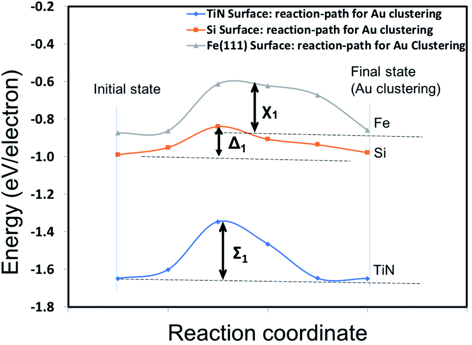 | ||
| Fig. 3 Au cluster formation pathways on Fe (111) (grey, triangles), Si (111) (orange, squares), and TiN (100) (blue, diamonds). The energy barriers for Au diffusion and cluster formation on Fe (111), Si (111), and TiN (100) are X1, Δ1, and Σ1, respectively. | ||
The effect of TiN on Si NW morphology was investigated by low-pressure chemical vapor deposition (LPCVD) of Si(P) NWs on SS304 and TiN/SS304 disks and subsequent SEM observations. LIB anode performances were evaluated, with a focus on fast lithiation in phosphorus doped n-type Si(P) NWs.31 Prior to the Si(P) NW growth, a 3 nm-thick Au layer was deposited onto SS304 and TiN/SS304 disks under the same conditions utilized for Au dot formation (Fig. 1 and 2). Fig. 4 shows the typical top- and 45° tilted-view SEM images of Si(P) NWs grown on SS304 and TiN/SS304 disks. The top-view SEM images (Fig. 4(a) and (c)) revealed NW growth and agglomerate formation on both SS304 and TiN surfaces. The number densities of NWs, estimated by counting in the top-view SEM images of 18 samples for each case, are 5–8 and 10–12 wires per µm2 for SS304 and TiN surfaces, respectively. The larger number density of NWs on TiN than on SS304 provides insight into either enhanced NW nucleation or suppressed bulk-like agglomerate formation on TiN. The tilted-view SEM images (Fig. 4(b) and (d)) reveal the dominant presence of chunks at the bottom of the samples grown on SS304. Fig. 4(c) shows that the chunks and short NWs, with >200 nm lateral size, prevailed on the surface of SS304. In contrast, Fig. 4(d) shows that a significant amount of the Si(P) NWs were not buried in chunks, but instead were attached directly to the TiN surface. Suppressed agglomeration of Au on TiN, as shown by Fig. 1–3, can be reasonably correlated with the higher number density of Au-catalyzed NWs on TiN.
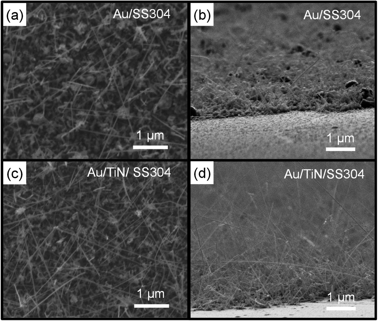 | ||
| Fig. 4 SEM images of Si(P) NWs grown on 3 nm-thick Au/SS304 disks (a, b) and 3 nm-thick Au/50 nm-thick TiN/SS304 disks (c, d). (a, c) and (b, d) show the top-view and 45° tilted-view images, respectively. | ||
The effects of the morphological differences of Si(P) NWs induced by TiN introduction were examined with respect to the electrochemical performances of Si-based LIB anodes, using specific gravimetric capacity measurements at various charging rates in a 2032 type half-coin cell configuration. There were no additives in the half-coin cell. Before the first cycle at a current rate of interest, each half-coin cell was cycled at a current rate of 200 mA g−1 (0.05C for Si) in the voltage windows of 0.005 and 1.5 V to form a conformal solid electrolyte interphase. Fig. 5(a) shows the specific gravimetric capacity curves of Si(P) NWs grown on SS304 and TiN/SS304 disks, along with the number of cycles at a current rate of 800 mA g−1 (0.2C for Si). The specific capacities of Si(P) NWs grown on SS304 and TiN/SS304 disks at the first cycle were 1720 and 2480 mA h g−1, respectively. The specific capacity of Si(P) NWs on TiN/SS304 decreased steadily during the cycling, whereas that on SS304 showed a two-step decrease. During the charging/discharging cycles up to 500 times, the specific capacity of Si(P) NWs on TiN/SS304 was noticeably larger than that on SS304. After the 500th-cycle of charging and discharging at 800 mA h g−1 (0.2C for Si), the specific capacity of Si(P) NWs grown on TiN/SS304 was 1000 mA h g−1 whereas that on SS304 was 230 mA h g−1. The retained ratio of specific capacities at the 500th-cycle to those from the 1st-cycle was 0.4 and 0.13 for TiN/SS304 and SS304, respectively. Cyclic voltammetry measurements show that TiN does not reversibly react with lithium within the potential range of the cell, and thus does not contribute to the enhanced retained capacity (see the ESI, Fig. S2†). The chemical inertness of TiN is consistent with reported results.32,33 Rate-dependent specific capacity was also used to assess LIB anode performance. Fig. 5(b) shows the rate-dependent specific gravimetric capacities of Si(P) NWs grown on TiN/SS304 and SS304 at various current rates ranging from 400 (0.1C for Si) to 8000 (2C for Si) mA g−1. For all current rates in the range of 400 and 8000 mA g−1, the specific capacities of Si(P) NWs grown on TiN/SS304 are 30–50% larger than those on SS304. The rate- and cycle-dependent electrochemical characterization revealed that introducing TiN as a substrate of Si(P) NWs significantly improved LIB anode performances in the case of direct growth of Si(P) NWs on a metal current collector. The improved LIB anode performances are attributed to the larger fraction of NWs than that of the bulk-like chunks. Reducing these bulk-like structures via suppressed agglomeration of nuclei for Si results in an increase in the fraction of NWs. The conductive diffusion barrier design could also be expanded to other current collectors such as carbon based and stainless-steel fibers aiming toward improved performance for various battery type applications.34–36 Consequently, Si NWs directly grown on a current collector enhance LIB anode performances with minimal hindrance from bulk-like structures.
 | ||
| Fig. 5 Specific gravimetric capacities of Si(P) NWs grown on SS304 (black, square, empty) and on TiN/SS304 (red, circle, solid) over cycling at 800 mA g−1 (0.2C for Si) (a) and at different charging rates (b). | ||
Conclusion
We achieved enhanced Si-based LIB anode performances via suppressed agglomeration of Au particles as nucleation sites of Si NWs. Energetics at the interface between Au and TiN led to the spontaneous formation of Au nanoparticles and minimal surface diffusion of Au on TiN. The underlying interfacial characteristics of the Au/TiN interface resulted in preferential nucleation of Si(P) NWs over the growth of bulk-like Si structures, such as chunks. A higher fraction of Si(P) NWs in the LIB anode improved Si-based LIB anode performances, in terms of rate-dependent specific gravimetric capacity and durability. Our method of Si NW growth on TiN provides a facile and economical way to realize high-performance LIB anodes due to the established deposition of TiN, which is widely employed in various industries and applications, such as semiconductor device manufacturing, machine tool fabrication, aerospace, and biomedical tools.Conflicts of interest
There are no conflicts to declare.Acknowledgements
This work was performed in part at CINT, a U.S. Department of Energy, Office of Basic Energy Sciences User Facility at Los Alamos National Laboratory (contract DE-AC52-06NA25396), and Sandia National Laboratories (contract DE-AC04-94AL85000). This work is also supported in part by the U.S. Department of Energy Basic Energy Sciences Core Program (LANL E3B5). This research used resources of the National Energy Research Scientific Computing Center, a DOE Office of Science User Facility (contract DE-AC02-05CH11231). The research was partly supported by the Laboratory Directed Research and Development Program of Los Alamos National Laboratory.References
- G. E. Blomgren, The development and future of lithium ion batteries, J. Electrochem. Soc., 2017, 164(1), A5019–A5025 CrossRef CAS.
- T. M. Gür, Review of electrical energy storage technologies, materials and systems: challenges and prospects for large-scale grid storage, Energy Environ. Sci., 2018, 11, 2696–2767 RSC.
- H. Wu and Y. Cui, Designing nanostructured Si anodes for high energy lithium ion batteries, Nano Today, 2012, 7, 414–429 CrossRef CAS.
- D. Larcher, S. Beattie, M. Morcrette, K. Edström, J.-C. Jumas and J.-M. Tarascon, Recent findings and prospects in the field of pure metals as negative electrodes for Li-ion batteries, J. Mater. Chem., 2007, 17, 3759–3772 RSC.
- L. Y. Beaulieu, T. D. Hatchard, A. Bonakdarpour, M. D. Fleischauer and J. R. Dahn, Reaction of Li with alloy thin films studied by in situ AFM, J. Electrochem. Soc., 2003, 150(11), A1457–A1464 CrossRef CAS.
- T. Kennedy, M. Brandon and K. M. Ryan, Advances in the application of silicon and germanium nanowires for high-performance lithium-ion batteries, Adv. Mater., 2016, 28, 5696–5704 CrossRef CAS PubMed.
- C. K. Chan, H. Peng, G. Liu, K. McIlwrath, X. F. Zhang, R. A. Huggins and Y. Cui, High-performance lithium battery anodes using silicon nanowires, Nat. Nanotechnol., 2008, 3, 31–35 CrossRef CAS PubMed.
- Z. Zhou, L. F. Ma and C. L. Tan, Preparation of Layered (NH4)2V6O16 center dot H2O Nanosheets as an Anode for Li-ion Batteries, Chem. J. Chin. Univ., 2021, 42(2), 662–670 Search PubMed.
- C. L. Tan, Z. Y. Zeng, X. Huang, X. H. Rui, X. J. Wu, B. Li, Z. M. Luo, J. Z. Chen, B. Chen, Q. Y. Yan and H. Zhang, Liquid-Phase Epitaxial Growth of Two-Dimensional Semiconductor Hetero-nanostructures, Angew. Chem., Int. Ed., 2015, 54(6), 1841–1845 CrossRef CAS PubMed.
- J.-H. Cho, X. Li and S. T. Picraux, The effect of metal silicide formation on silicon nanowire-based lithium-ion battery anode capacity, J. Power Sources, 2012, 205, 467–473 CrossRef CAS.
- S. W. Lee, M. T. McDowell, L. A. Berla, W. D. Nix and Y. Cui, Fracture of crystalline silicon nanopillars during electrochemical lithium insertion, Proc. Natl. Acad. Sci. U. S. A., 2012, 109(11), 4080–4085 CrossRef CAS PubMed.
- J.-H. Cho and S. T. Picraux, Enhanced lithium ion battery cycling of silicon nanowire anodes by template growth to eliminate silicon underlayer islands, Nano Lett., 2013, 13(11), 5740–5747 CrossRef CAS PubMed.
- M. Kolíbal, T. Pejchal, T. Musálek and T. Šikola, Catalyst–substrate interaction and growth delay in vapor–liquid–solid nanowire growth, Nanotechnology, 2018, 29, 205603 CrossRef PubMed.
- B. Ressel, K. C. Prince, S. Heun and Y. Homma, Wetting of Si surfaces by Au–Si liquid alloys, J. Appl. Phys., 2003, 93, 3886–3892 CrossRef CAS.
- V. Zannier, V. Grillo, F. Martelli, J. R. Plaisier, A. Lausi and S. Rubini, Tuning the growth mode of nanowires via the interaction among seeds, substrates and beam fluxes, Nanoscale, 2014, 6, 8392–8399 RSC.
- B. Nikoobakht, A. Herzing, S. Muramoto and J. Tersoff, Vapor–liquid–solid etch of semiconductor surface channels by running gold nanodroplets, Nano Lett., 2015, 15(12), 8360–8364 CrossRef CAS PubMed.
- X. Li, J.-H. Cho, N. Li, Y. Zhang, D. Williams, S. A. Dayeh and S. T. Picraux, Carbon Nanotube-Enhanced Growth of Silicon Nanowires as an Anode for High-Performance Lithium-Ion Batteries, Adv. Energy Mater., 2012, 2(1), 87–93 CrossRef CAS.
- D. W. Pashley and M. J. Stowell, Nucleation and growth of thin films as observed in the electron microscope, J. Vac. Sci. Technol., 1966, 3(3), 156–166 CrossRef CAS.
- M.-A. Nicolet, Diffusion barriers in thin films, Thin Solid Films, 1978, 52, 415–443 CrossRef CAS.
- K. G. Grigorov, G. I. Grigorov, M. Stoyanova, J.-L. Vignes, J.-P. Langeron, P. Denjean and J. Perriere, Diffusion of silicon in titanium nitride films. Efficiency of TiN barrier layers, Appl. Phys. A, 1992, 55, 502–504 CrossRef.
- K. Kishino, H. Sekiguchi and A. Kikuchi, Improved Ti-mask selective-area growth (SAG) by rf-plasma-assisted molecular beam epitaxy demonstrating extremely uniform GaN nanocolumn arrays, J. Cryst. Growth, 2009, 311(7), 2063–2068 CrossRef CAS.
- M. Wölz, C. Hauswald, T. Flissikowski, T. Gotschke, S. Fernández-Garrido, O. Brandt, H. T. Grahan, L. Geelhaar and H. Riechert, Epitaxial growth of GaN nanowires with high structural perfection on a metallic TiN film, Nano Lett., 2015, 15, 3743–3747 CrossRef PubMed.
- E. B. Watkins, J. Majewski, J. K. Baldwin, Y. Chen, N. Li, R. G. Hoagland, S. K. Yadav, X.-Y. Liu, I. J. Beyerlein and N. A. Mara, Neutron reflectometry investigations of interfacial structures of Ti/TiN layers deposited by magnetron sputtering, Thin Solid Films, 2016, 616, 399–407 CrossRef CAS.
- N. Li, H. Wang, A. Misra and J. Wang, In situ nanoindentation study of plastic co-deformation in Al-TiN nanocomposites, Sci. Rep., 2014, 4, 6633 CrossRef CAS PubMed.
- L. Vitos, A. V. Ruban, H. L. Skriver and J. Kollár, The surface energy of metals, Surf. Sci., 1998, 411, 186–202 CrossRef CAS.
- C.-C. Sun, S.-C. Lee, W.-C. Hwang, J.-S. Hwang, I.-T. Tang and Y.-S. Fu, Surface free energy of alloy nitride coatings deposited using closed field unbalanced magnetron sputter ion plating, Mater. Trans., 2006, 47(10), 2533–2539 CrossRef CAS.
- F. R. de Boer, R. Boom, W. C. M. Mattens, A. R. Miedema and A. K. Niessen, Cohesion in Metals, North-Holland, Amsterdam, 1988 Search PubMed.
- J. J. Gilman, Direct measurements of the surface energies of crystals, J. Appl. Phys., 1960, 31, 2208 CrossRef CAS.
- E. A. Brandes and G. B. Brook, Smithells Metals Reference Book, 7th edn, Butterworth-Heinemann, 2003 Search PubMed.
- M.-Y. Li, M. Sui, E.-S. Kim and J. Lee, Effect of Au thickness on the evolution of self-assembled Au droplets on GaAs (111)A and (100), Nanoscale Res. Lett., 2014, 9, 407 CrossRef PubMed.
- X. H. Liu, L. Q. Zhang, L. Zhong, Y. Liu, H. Zheng, J. W. Wang, J.-H. Cho, S. A. Dayeh, S. T. Picraux, J. P. Sullivan, S. X. Mao, Z. Z. Ye and J. Y. Huang, Ultrafast electrochemical lithiation of individual Si nanowire anodes, Nano Lett., 2011, 11(6), 2251–2258 CrossRef CAS PubMed.
- X. Zhao, Q. Zhou, H. Ming, J. Adkins, M. Liu, L. Su and J. Zheng, Surface nitridation induced high electrochemical performance of Li4Ti5O12 using urea as a nitrogen source, Ionics, 2013, 19(12), 1843–1848 CrossRef CAS.
- D. Tang, R. Yi, M. L. Gordin, M. Melnyk, F. Dai, S. Chen, J. Song and D. Wang, Titanium nitride coating to enhance the performance of silicon nanoparticles as a lithium-ion battery anode, J. Mater. Chem. A, 2014, 2(27), 10375–10378 RSC.
- S. Imtiaz, I. S. Amiinu, D. Storan, N. Kapuria, H. Geaney, T. Kennedy and K. M. Ryan, Dense Silicon Nanowire Networks Grown on a Stainless-Steel Fiber Cloth: A Flexible and Robust Anode for Lithium-Ion Batteries, Adv. Mater., 2021, 33(52), 2105917 CrossRef CAS PubMed.
- N. Harpak, G. Davidi, D. Schneier, S. Menkin, E. Mados, D. Golodnitsky, E. Peled and F. Patolsky, Large-Scale Self-Catalyzed Spongelike Silicon Nano-Network-Based 3D Anodes for High-Capacity Lithium-Ion Batteries, Nano Lett., 2019, 19(3), 1944–1954 CrossRef CAS PubMed.
- N. Harpak, G. Davidi and F. Patolsky, Breathing parylene-based nanothin artificial SEI for highly-stable long life three-dimensional silicon lithium-ion batteries, Chem. Eng. J., 2022, 429, 132077 CrossRef CAS.
Footnotes |
| † Electronic supplementary information (ESI) available. See DOI: 10.1039/d1na00844g |
| ‡ Present address: Pacific Northwest National Laboratory, Richland, WA, 99354, USA. |
| § Present address: Interdisciplinary Materials Measurement Institute, Korea Research Institute of Standards and Science (KRISS), Daejeon 34113, Republic of Korea. |
| This journal is © The Royal Society of Chemistry 2022 |