
 Open Access Article
 This Open Access Article is licensed under a Creative Commons Attribution-Non Commercial 3.0 Unported Licence
Modulation of electrical properties in MoTe2 by XeF2-mediated surface oxidation†
Eunji
Ji‡
a,
Jong Hun
Kim‡
ade,
Wanggon
Lee
b,
June-Chul
Shin
d,
Hyungtak
Seo
 c,
Kyuwook
Ihm
f,
Jin-Woo
Park
a and
Gwan-Hyoung
Lee
*degh
c,
Kyuwook
Ihm
f,
Jin-Woo
Park
a and
Gwan-Hyoung
Lee
*degh
aDepartment of Material Science and Engineering, Yonsei University, Seoul, 03722, Korea
bDepartment of Energy Systems Research, Ajou University, Suwon 16499, Republic of Korea
cDepartment of Materials Science and Engineering, Ajou University, Suwon 16499, Republic of Korea
dDepartment of Materials Science and Engineering, Seoul National University, Seoul 08826, Korea
eResearch Institute of Advanced Materials (RIAM), Seoul National University, Seoul 08826, Korea
fDepartment of Physics and Pohang Accelerator Laboratory, Pohang University of Science and Technology, 37673, Pohang, Korea
gInstitute of Engineering Research, Seoul National University, Seoul 08826, Korea
hInstitute of Applied Physics, Seoul National University, Seoul 08826, Korea. E-mail: gwanlee@snu.ac.kr
First published on 5th January 2022
Abstract
Transition metal dichalcogenides (TMDs) are promising candidates for the semiconductor industry owing to their superior electrical properties. Their surface oxidation is of interest because their electrical properties can be easily modulated by an oxidized layer on top of them. Here, we demonstrate the XeF2-mediated surface oxidation of 2H-MoTe2 (alpha phase MoTe2). MoTe2 exposed to XeF2 gas forms a thin and uniform oxidized layer (∼2.5 nm-thick MoOx) on MoTe2 regardless of the exposure time (within ∼120 s) due to the passivation effect and simultaneous etching. We used the oxidized layer for contacts between the metal and MoTe2, which help reduce the contact resistance by overcoming the Fermi level pinning effect by the direct metal deposition process. The MoTe2 field-effect transistors (FETs) with a MoOx interlayer exhibited two orders of magnitude higher field-effect hole mobility of 6.31 cm2 V−1 s−1 with a high on/off current ratio of ∼105 than that of the MoTe2 device with conventional metal contacts (0.07 cm2 V−1 s−1). Our work shows a straightforward and effective method for forming a thin oxide layer for MoTe2 devices, applicable for 2D electronics.
Introduction
Transition metal dichalcogenide (TMD) semiconductors have been actively studied owing to their great potential in advanced electronics and unprecedented physical properties.1–8 Electronic devices based on exfoliated TMDs have a thickness limit of a few atomic layers with dangling-bond-free passivated surfaces because individual layers of TMDs are held together with weak van der Waals forces. Among these TMDs, 2H-MoTe2 (alpha phase MoTe2) has a moderate indirect band gap (Eg) of 0.88 eV in bulk9,10 and a direct band gap (Eg) of 1.1 eV in a monolayer form.11 The moderate band gap of MoTe2, similar to that of bulk silicon, makes it a promising candidate for various electronic applications, such as transistors, complementary logic devices, optoelectronic devices, and memory.12,13 It is well known that the Schottky barrier height between MoTe2 and the metal is very weakly dependent on the work function of the metal due to the strong Fermi level pinning effect, leading to a high contact resistance (Rc).14 Although the Schottky barrier height is determined by the work function of the contact metal according to the Schottky–Mott rule, a strong Fermi level pinning effect and high contact resistance (Rc) are caused by physical bombardment during the metal deposition process, leading to crystallinity damage in MoTe2.15 It was recently found that transition metal oxides (TMOs) are suitable candidates as buffer layers between TMDs and metals.16,17 The fabrication of TMOs has been reported using various methods, such as oxygen plasma treatment,18 atomic layer deposition (ALD),19 UV–ozone treatment20 and thermal evaporation.21 However, surface treatment methods can easily damage TMDs, leading to reduced crystallinity and increased surface roughness.15,22 The atomic thickness of TMD flakes gives rise to these issues, degrading the electronic properties of the device.In this work, we demonstrate the fabrication of a thin and uniform oxidized layer on top of MoTe2 by exposing it to XeF2 gas. The oxidized layer had a uniform thickness of ∼2.5 nm regardless of the exposure time (within ∼120 s) due to the passivation effect and simultaneous etching. The non-stoichiometric oxide layer has a high work function, allowing for p-doping of the underlying MoTe2. The MoTe2 device showed a high field-effect hole mobility of 6.31 cm2 V−1 s−1 with a high on/off current ratio of ∼105. The palladium (Pd) metal can easily tunnel to MeTe2 layer by MoOx layer. The mobility is two orders of magnitude higher than that of the MoTe2 device with conventional metal contacts.
Results and discussions
The mechanically exfoliated MoTe2 flakes were exposed to XeF2 gas at 1.8 torr for different treatment times. The optical microscope images of the MoTe2 flakes in Fig. 1a show the contrast change before and after XeF2 exposure for 150 s. The corresponding surface morphology was also identified by using atomic force microscopy (AFM), as shown in Fig. 1b. As confirmed using AFM images, even after the treatment, the overall structure was not changed, exhibiting the relatively uniform surface morphologies; however, the optical contrast of the flakes was significantly suppressed after XeF2 exposure. The depression in the optical contrast may be attributed to the change in the optical path caused by mediating the refractive properties of MoTe2 with XeF2 treatment.23,24Fig. 1c shows the height profiles created by following the dashed lines in Fig. 1b. The thickness of the fourth layer (4 L) and third layer (3 L) MoTe2 was measured to be ∼3.1 nm and ∼2.4 nm before XeF2 exposure (blue dashed lines in Fig. 1b), respectively. However, the thickness remained approximately the same even after XeF2 exposure (red dashed lines in Fig. 1b), i.e., ∼3.0 nm and ∼2.3 nm, respectively. Fig. 1d and e show the Raman spectra of the 3 L and 4 L regions (blue and red dots in Fig. 1a, respectively) of the MoTe2 flakes. MoTe2 showed the representative phonon modes of Ag1 (∼170 cm−1), E2g1 (∼234 cm−1), and B2g1 (∼289 cm−1).25 Meanwhile, monolayer (1 L) MoTe2 was found to have a prominent peak of E2g1 and a weaker peak of A1g at ∼235 cm−1 and ∼174 cm−1, respectively.26 The Raman spectra of 3 L MoTe2 in Fig. 1d show that all Raman modes were depressed after XeF2 exposure. However, only the B2g1 mode of 4 L MoTe2 disappeared after XeF2 exposure, maintaining other Raman peaks (Fig. 1e). This indicates that a few topmost layers of MoTe2 were substituted with a different material with a comparable atomic thickness, while the subsurface remained as MoTe2. It was expected that unidentified layers were produced upon XeF2 exposure. In particular, the Raman mode related to MoO3![[thin space (1/6-em)]](https://www.rsc.org/images/entities/char_2009.gif) 27 and MoO228,29 cannot be observed. Therefore, Raman spectroscopy failed to provide clear evidence of it.
27 and MoO228,29 cannot be observed. Therefore, Raman spectroscopy failed to provide clear evidence of it.
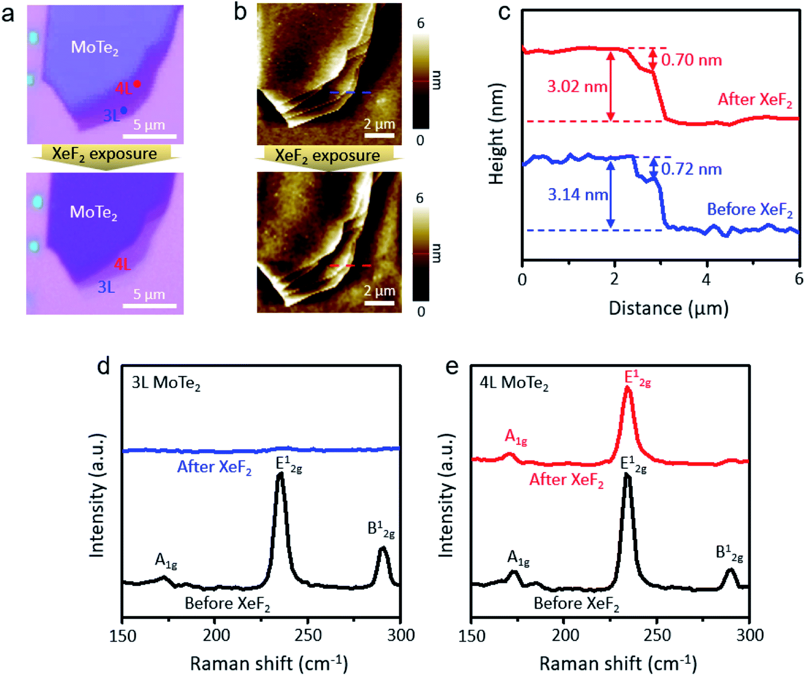 | ||
| Fig. 1 (a) Optical microscope images of few layer MoTe2 before and after XeF2 exposure at 1.8 torr for 150 s, (b) AFM topology images of MoTe2 before and after XeF2 treatment, (c) height profile of MoTe2 before (blue line) and after (red line) XeF2 treatment, (d) the Raman spectra of 3 L MoTe2 (blue dot region) in Fig. 1a before (black line) and after (red line) XeF2 treatment, and (e) the Raman spectra of 4 L MoTe2 (red dot region) in Fig. 1a before (black line) and after (red line) XeF2 treatment. | ||
ESI, Fig. S2a and b† show the optical microscope images and Raman spectra of 1 L and 2 L of MoTe2 before and after XeF2 exposure at 1.8 torr for 60 s, respectively. After XeF2 treatment, the intensities of E2g1 and B2g1 in 2 L MoTe2 were slightly lower than those before XeF2 exposure. However, the B2g1 mode in 2 L disappeared after XeF2 exposure in the Raman spectrum, indicating that 2 L transforms into 1 L at 1.8 torr for 60 s (the graph at the top in the red-colored region in ESI, Fig. S2b†). All modes in 1 L of MoTe2 disappeared after XeF2 exposure, indicating that its crystal structure vanished (the graphs in the blue-colored region of ESI, Fig. S2b†). The E2g1 mode of XeF2-exposed 2 L was downshifted by 2.18 cm−1 compared to that of pristine 1 L of MoTe2 (before XeF2 exposure). The Ag1 mode showed an upshift from 171.94 cm−1 (pristine 1 L of MoTe2) to 172.15 cm−1 (XeF2-exposed 2 L of MoTe2), which is another evidence for p-type doping of MoTe2 after XeF2 treatment.30 We used the Raman mapping method to verify the uniform treatment of XeF2 gas on the MoTe2 surface (ESI, Fig. S2c and d,†). E2g1 and B2g1 intensities uniformly disappeared and remained after XeF2 exposure. In particular, the E2g1 intensity remained and B2g1 mode completely disappeared in the 2 L region after XeF2 exposure, implying that 2 L becomes uniform 1 L.
Scanning transmission electron microscopy (STEM) was used to identify the mysterious top layer of XeF2-exposed MoTe2. As shown in the cross-sectional STEM images of Fig. 2a, two MoTe2 samples with different XeF2 exposure times of 60 and 120 s at 1.8 torr showed a uniform and smooth layer of the same thickness (∼2.5 nm) on top of intact MoTe2. The underlying MoTe2 might have remained intact, without any structural changes, even after XeF2 exposure. The surface was continuously scanned using contact-mode AFM to evaluate the thickness of the oxidized layer. The topmost region of XeF2-exposed MoTe2 can be smoothly removed by using an AFM tip, as shown in Fig. 2b. The height profile based on the red dashed lines in Fig. 2b is shown in Fig. 2d. The exposed new surface had a difference in thickness of ∼2.6 nm compared to the unexposed surface, which is consistent with the TEM results. The peeled area appeared as flat as the non-peeled area. In addition, the energy-dispersive X-ray spectroscopy (EDS) map in Fig. 2c clearly shows that the top region of XeF2-exposed MoTe2 contains more oxygen than the underlying region. Although it was challenging to quantitatively analyze the composition of the top region due to the resolution limit of the EDS and ultrathin sample, we could confirm that the top region of MoTe2 was predominantly oxidized and disordered by XeF2-exposure (a green dotted region indicates oxygen), while the lower MoTe2 remained approximately intact even after XeF2 exposure, showing only the Mo (purple dots) and Te (cyan-colored dots) spectra in EDS.
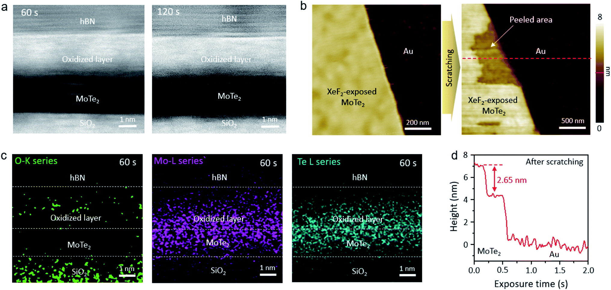 | ||
| Fig. 2 (a) Cross-sectional STEM images of MoTe2 after XeF2 treatment at 1.8 torr for 60 s and 120 s, respectively, (b) AFM topology images of XeF2 treated MoTe2 before and after removing the surface layer by using a cantilever tip, (c) EDS mapping image of O-K, Mo-L and Te-L series of MoTe2 after XeF2 treatment at 1.8 torr for 60 s and (d) height profile of XeF2 treated MoTe2 after scratching by using a cantilever tip. | ||
The AFM images in Fig. 3a show the surface morphology of XeF2-exposed MoTe2 for different times. The surface of XeF2-exposed MoTe2 is cleaner and smoother than plasma-treated MoTe2 for a long exposure time of 270 s owing to the suppression of ion-bombardment effect.31,32 The roughness and relative thickness of XeF2-exposed MoTe2 are plotted in Fig. 3b and c, respectively. The actual thicknesses of the flakes were measured using contact AFM. We did not observe a significant difference in the roughness of MoTe2 even after a long exposure of 270 s (Fig. 3b). Thermodynamically, the XeF2-treatment is possible to remove Mo or Te from the surface because the melting temperatures of MoF6 and TeF6 are lower than the room temperature.33 Therefore, if a few top layers of MoTe2 reacted with XeF2, it would turn into a disordered structure with several broken bonds. Moreover, the disordered layer can be easily oxidized by exposing it to air after treating the surface with XeF2 gas. Therefore, the broken structures can easily bond with oxygen when the sample is unloaded from the chamber. Some Mo–O bonds were expected to form at the surface defect sites, thinning the intrinsic MoTe2.34 In Fig. 3c, the relative thickness (the difference in thickness before and after XeF2 exposure) was plotted as a function of the treatment time. The relative thickness of MoTe2 gradually increased with the treatment time (from 0 to 120 s) after XeF2 exposure because of the self-limiting growth mechanism of MoOx.35,36 This is consistent with the results illustrated in Fig. 2a (similar thicknesses of the oxidized layer after XeF2 exposure for 60 and 120 s). However, the relative thickness decreased rather rapidly with the exposure time from 120 to 270 s. The formation of MoF6 in the chamber can become more dominant than MoOx due to the Gibbs free energies of MoF6, MoO2, and MoO3 (i.e., −1473.17, −533.0, and −668.1 J mol−1, respectively).33 Therefore, such a decrease in the thickness can be observed as MoF6 can be easily removed owing to its low melting and boiling temperatures. When the available number of fluorine atoms decreased at a reduced pressure of 1 torr-60 s XeF2 (ESI, Fig. S3a and b,†), the number of bonding between carbon (C) and fluorine (F) atom should be limited, which revealed the nanohole surface on the MoTe2 surface. In this case, while the relative thickness was just negligibly changed (ESI, Fig. S3d†), the surface roughness became deteriorated, as shown in ESI, Fig. S3c.† We used the same conditions—fabrication of a uniform oxidized layer with no nanoholes on MoTe2 with XeF2 gas of 1.8 torr—for other experiments. Changes in the morphology due to various treatments in 2D materials devices often lead to reduced electrical contact.37–39 We directly fabricated smooth and uniform oxidized layers on MoTe2 through XeF2 gas under the conditions of 1.8 torr within 120 s. The XeF2 exposure method is easier to scale-up compared with previous methods, such as laser, plasma and thermal annealing.40–42
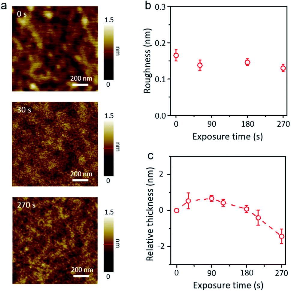 | ||
| Fig. 3 (a) The AFM topology images of XeF2 exposed MoTe2 to show the uniform surface morphology after XeF2 treatment for 0 s (as-exfoliated MoTe2), 30 s and 270 s, respectively, (b) the root-mean-square (RMS) roughness of MoTe2 after XeF2 treatment at 1.8 torr with appropriate exposure times (from 0 s to 270 s) and (c) the relative height change of MoTe2 as a function of increasing XeF2 treatment time at 1.8 torr. | ||
Photoelectron spectroscopy (PES) with a photon energy of 780 eV was performed under ultra-high vacuum conditions to identify the top layer of MoTe2 before (black dotted lines) and after (red dotted lines) exposure to XeF2 (Fig. 4a–d). In each figure, the top-(bottom-) panel shows the core-level spectrum before (after) the treatment. We note that the MoTe2 flakes were treated with XeF2 gas at 1.8 torr for 60 s for PES-characterization. The Mo 3d core level from MoTe2 showed the binding energies of Mo 3d5/2 at 228.4 eV and Mo 3d3/2 at 231.9 eV before XeF2 exposure, agreeing with the previous report (Fig. 4a).43 This indicates that the as-prepared MoTe2 sample has high crystallinity. However, mixed states of Mo4+ and Mo6+ were observed after XeF2 exposure of 60 s (red dotted lines), supporting the partial oxidation of molybdenum. Additionally, the Te–O bonds in the XPS spectra showed two peaks at 576.3 eV and 587.1 eV (upper graph of Fig. 4b, red dotted lines). The more interesting result is that the Mo 3d and Te 3d peaks are downshifted to almost the same extent (∼0.7 eV). The peak downshifts can be assigned to hole-doping, since the Fermi level, which represents zero energy, moves further away from the conduction band with hole-doping.44,45 Besides, the previously suggested Raman spectra also support that the p-type doping occurred after XeF2 exposure (ESI, Fig. S2b†). As expected, the O 1s core level appeared after XeF2 exposure (Fig. 4c). No peak related to H2O (∼532 eV30) was found because PES was performed under ultra-high vacuum conditions immediately after mechanically exfoliating MoTe2. The O 1s core-level spectrum together with the occurrence of Mo6+ in Mo 3d strongly indicates that an oxidized layer was formed, such as MoOx.46 Lastly, the F 1s peak (Fig. 4d) shows that a small number of fluorine atoms are chemically bonded. Hence, MoOx, a disordered oxide layer containing negligible fluorine atoms, was formed, playing an important role in doping.
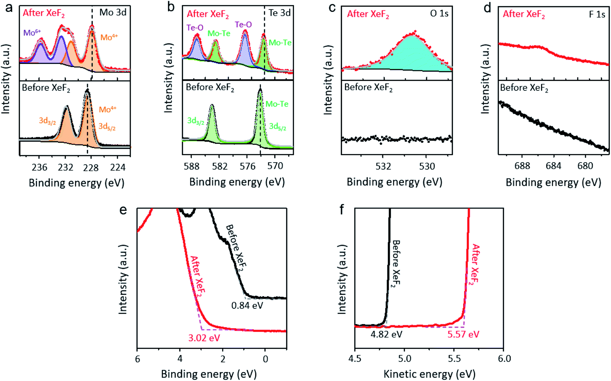 | ||
| Fig. 4 (a–d) PES spectra with a photon energy of 780 eV of 2H-MoTe2 without and with XeF2 treatment at 1.8 torr for 60 s; the bottom spectra of PES show MoTe2 before XeF2 treatment and the top spectra of PES show that after XeF2 treatment at 1.8 torr for 60 s. (a) Mo 3d spectra, (b) Te 3d spectra, (c) O 1s spectra and (d) F 1s spectra. (e and f) PES (hv = 90 eV) of 2H-MoTe2 without and with XeF2 treatment at 1.8 torr for 60 s; the black lines show the spectra of PES before XeF2 treatment and the red lines show the spectra of PES after XeF2 treatment at 1.8 torr for 60 s. (e) The valence edge of MoTe2 before and after XeF2 exposure and (f) the secondary electron cutoffs of MoTe2 before and after XeF2 exposure. | ||
The valence band edges of the samples were investigated using PES (hv = 90 eV), as shown in Fig. 4e. The valence band edge of MoTe2 before (black) and after (red) XeF2 exposure was found to be positioned at ∼0.8 eV and ∼3.0 eV below the Fermi level, respectively. The valence band edge of XeF2-treated MoTe2 shifted to about 3.0 eV, which is close to the value of the MoOx phase.47 Interestingly, MoOx does not contain a high density of defects (gap states) inside both MoTe2 surfaces before (black) and after (red) XeF2 exposure. The ultrathin oxidized layer can completely change the band diagram. Also, the secondary electron cutoffs (Fig. 4f) show that the work functions of the samples were positioned at ∼4.8 (pristine MoTe2) and ∼5.6 eV (MoOx), respectively, due to the formation of a non-stoichiometric oxidation phase after XeF2 exposure. The work function of XeF2-exposed MoTe2 was smaller than that (∼6.8 eV) of MoO3.48 Therefore, the result indicates that only a few topmost surface layers of MoTe2 (3 L in Fig. 1) were substituted with MoOx with a comparable atomic thickness, while the subsurface (1 L in Fig. 1) still remained as MoTe2; however, the overall thickness was scarcely changed by XeF2-treatment within a limited exposure time. A schematic image of MoTe2 before and after XeF2 exposure is shown in ESI, Fig. S4.† The 4 L of MoTe2 was converted to a 1 L of MoTe2 with an oxidized layer at 1.8 torr for 150 s. The 3 L of the MoTe2 crystal structure disappeared after XeF2 exposure, forming the remaining oxidized layer.
We fabricated MoTe2 FETs by forming contacts in the XeF2-exposed regions because the ultrathin oxidized layer of XeF2-exposed MoTe2 can be used as a buffer layer between MoTe2 and the metal. Multilayer MoTe2 with a thickness of ∼3 nm was used for device fabrication. Two different types of contacts were fabricated on the same MoTe2 flakes (ESI, Fig. S5† shows the detailed device fabrication process). Electrodes were patterned by e-beam lithography and exposed to XeF2 for 60 s, followed by e-beam deposition of metals (Cr 1 nm/Pd 30 nm/Au 40 nm) to fabricate the contacts in the XeF2-exposed regions. Cr is an adhesion layer; Pd can be connected to MoTe2 for p-type FETs. Metals were also deposited on the surface of the pristine MoTe2 for comparison. As shown in Fig. 5a, the MoTe2 FET with conventional metal contacts showed a low field-effect hole mobility of 0.07 cm2 V−1 s−1 with an on/off current ratio of ∼104, probably because of the high contact resistance (see the non-linear output curves (Ids–Vds) in the inset). Furthermore, the MoTe2 FET with XeF2-exposed contacts exhibited two orders of magnitude higher hole mobility (6.31 cm2 V−1 s−1) with a higher on/off current ratio of ∼105. Particularly, the linear output curves in the inset of Fig. 5b show the ohmic nature of XeF2-exposed contacts. The linear-scale transfer curves of the two devices in Fig. 5c clearly show that the on-current of the MoTe2 FET with XeF2-exposed contacts is significantly higher than that of the MoTe2 FET with conventional metal contacts. The type and height of the Schottky barrier formed at the contact between the metal and the TMDs can determine the contact resistivity. However, the metal-insulator-semiconductor structure with an ultrathin insulating layer can substantially relieve the Fermi level pinning effect by reducing the direct metal contact to the interfacial states of MoTe2.49 The XeF2 vapor process can chemically react with only a few topmost layers of TMDs, minimizing the degradation of underlying MoTe2 crystallinity.34 In addition, the oxidized layer induces p-doping of the underlying MoTe2. Therefore, the ultrathin oxide interlayer enables overcoming the Schottky barrier induced by Fermi level pinning at the semiconductor–metal junction, reducing the contact resistance in the MoTe2 devices (see the band diagram in Fig. 5d). The uniform oxide interlayer only with several nm-thickness can be easily and precisely produced through our method. In particular, the oxygen plasma treatment method was suitable for scale up, but uniform surface cannot be achieved due to ion bombardment on the MoTe2 surface.35 Laser treatment is also widely used to improve the properties of contact between the metal and MoTe2,50 but there is a limitation to scale up. Therefore, our XeF2-mediated oxidation technique is a promising candidate for fabricating high-performance electronic devices based on MoTe2.
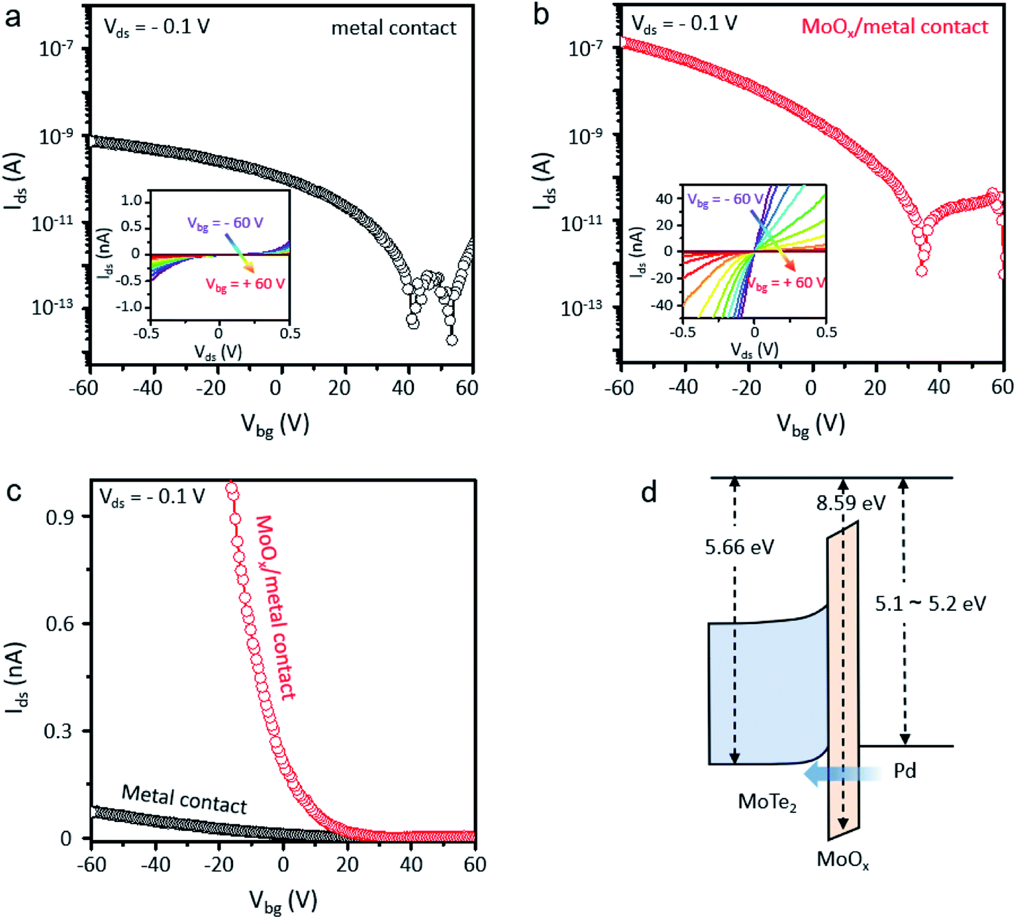 | ||
| Fig. 5 (a) Ids–Vg transfer characteristics of MoTe2 FETs with and without the XeF2 treatment process in the logarithmic scale. The black dotted line curve shows the transfer characteristics of the MoTe2 channel with direct contact between the metal and MoTe2. (b) The red dotted line curve shows the transfer characteristics of the MoTe2 channel with contact between the metal and MoOx/MoTe2 in the logarithmic scale. The insets of Fig. 5a and b show Ids–Vds output characteristics of the MoTe2 FET without XeF2 treatment in the contact region (Fig. 5a) and with XeF2 treatment in the contact region (Fig. 5b) before metal deposition. (c) Ids–Vg transfer characteristics of MoTe2 FETs both conventional metal contacts (black dots) and MoOx/metal contacts (red dots) in the linear scale and (d) the schematic image of the band diagram for MoTe2,15 oxidized layer, and Pd.21,51,52 | ||
Conclusions
In conclusion, we demonstrate a controllable technique to produce a uniform oxidized layer on top of MoTe2 by XeF2 exposure. XeF2-exposed MoTe2 was formed with a thin and uniform oxidized layer (∼2.5 nm-thick MoOx) regardless of the exposure time (within ∼120 s) because of the passivation effect and simultaneous etching. We could directly fabricate the ultra-smooth thin oxidized layer on MoTe2 by the simple and easy XeF2 vapor exposure method. In addition, the electrical properties of MoTe2 FETs with and without XeF2 treatment in the contact region were measured, including the hole mobility and on/off current ratio. The MoTe2 FET with an ultra-smooth MoOx interlayer shows a relatively high field-effect hole mobility of 6.31 cm2 V−1 s−1 with a high on/off current ratio of ∼105. This result is two orders of magnitude higher than that of MoTe2 FETs with conventional metal contacts (0.07 cm2 V−1 s−1). The simplicity and applicability of our method will be useful for practical applications of MoTe2 FETs in the future.Experimental section
Sample preparation
MoTe2 was mechanically exfoliated onto the SiO2 (280 nm)/Si substrate after the substrate was cleaned with acetone and isopropyl alcohol (IPA) in an ultra-sonication bath for 10 min, respectively. The exfoliated MoTe2 flakes were loaded into a XeF2 chamber (ESI, Fig. S1†). The XeF2 gas of high pressure (1.8 torr) was introduced into the chamber in a cyclic manner, where the chamber was filled with XeF2 for different treatment times in a cycle and then pumped out.Raman spectroscopy
The optical properties of MoTe2 were observed through Raman spectroscopy (Renishaw, inVia), with a laser wavelength of 532 nm and a spot size of ∼1 μm. Raman spectra at the same position on MoTe2 were obtained before and after XeF2 exposure.Atomic force microscopy (AFM)
Atomic force microscopy (AFM, Park systems, NX10) was used to observe the surface morphology, roughness, and thickness of the MoTe2 samples. The contact mode was used for exact thickness information. A silicon tip with an elastic constant of ∼0.2 N m−1 was used in contact mode.Transmission electron microscopy (TEM)
For cross-sectional TEM, a focused ion beam (FIB) system (Helios G4, Thermo Fisher Scientific, USA) was used. To protect the sample surface from e-beam, the XeF2-exposed MoTe2 flakes were covered with multilayer h-BN. We used TEM (JEM-F200, JEOL Ltd, Japan) with a low operating voltage of 80 keV. Transmission electron microscopy-energy dispersive X-ray spectroscopy (TEM-EDS) was used to analyze the atomic ratios.Photoemission spectroscopy (PES)
MoTe2 crystals were prepared on an Au-coated SiO2 substrate. Photoelectron spectroscopy (PES) spectra of the sample were recorded at hv = 780 eV. In addition, valence spectra and secondary electron cutoff were measured using a photon energy of hv = 90 eV. Synchrotron-based PES spectroscopy was performed at room temperature at the 4D beamline in the Pohang Light Source II (PLS II), Korea.Device fabrication and electrical measurements
MoTe2 field-effect transistors (FETs) were fabricated on a SiO2 (285 nm)/Si substrate using e-beam lithography (EBL, TESCAN). Metal contacts were deposited by using an e-beam evaporator (Temescal six pocket e-beam evaporation systems). The MoTe2 FETs were measured by using a semiconductor parameter analyzer (Keithley 4200). The source-drain current (Ids) was measured with a fixed source-drain voltage (Vds) of −0.1 V and varying back-gate voltage (Vbg) from −60 V to 60 V. The field-effect mobility (μFE) was calculated, extracting from the linear area of the transfer curve. The equation is μFE = [(ΔIds/ΔVbg)(L/W)Vds]/Cox, where Δ, W, L, and Cox are the gradient of Ids to Vds, channel width, length and gate capacitance of SiO2 (12.1 nF cm−2 for a SiO2 thickness of 285 nm).Author contributions
E. J. and J. H. K. contributed equally. E. J., J. H. K., and G. -H. L. designed this work. E. J. and J. H. K. performed all experiments including AFM, Raman spectroscopy, PES, and STEM analysis. W. L. performed the Xenon difluoride (XeF2) experiments. K. I performed the photoemission spectroscopy (PES) system. E. J. and J.-C. S fabricated the device and analyzed device performance. All authors discussed the results. E. J. and J. H. K. wrote the manuscript together. J.-W. P, H. S and G.-H. L reviewed and edited the manuscript together. All authors have given approval to the final version of the manuscript.Conflicts of interest
The authors declare no competing financial interest.Acknowledgements
This research was supported by the Basic Science Research Program through the National Research Foundation of Korea (NRF) funded by the Ministry of Science, ICT & Future Planning (2021R1A2C3014316) and the National Research Foundation of Korea (NRF) funded by the Ministry of Science and ICT (2021M3F3A2A01037858). Experiments at PLS-II were supported by MSIP-R. O., Korea. This paper was also a result of the research project supported by SK Hynix Inc.References
- B. Radisavljevic, A. Radenovic, J. Brivio, V. Giacometti and A. Kis, Nat. Nanotechnol., 2011, 6, 147–150 CrossRef CAS PubMed.
- Z. Yin, H. Li, H. Li, L. Jiang, Y. Shi, Y. Sun, G. Lu, Q. Zhang, X. Chen and H. Zhang, ACS Nano, 2012, 6, 74–80 CrossRef CAS PubMed.
- S. Fathipour, N. Ma, W. Hwang, V. Protasenko, S. Vishwanath, H. Xing, H. Xu, D. Jena, J. Appenzeller and A. Seabaugh, Appl. Phys. Lett., 2014, 105, 192101 CrossRef.
- J. Y. Lim, M. Kim, Y. Jeong, K. R. Ko, S. Yu, H. G. Shin, J. Y. Moon, Y. J. Choi, Y. Yi and T. Kim, npj 2D Mater. Appl., 2018, 2, 1–7 CrossRef CAS.
- N. Huo, S. Tongay, W. Guo, R. Li, C. Fan, F. Lu, J. Yang, B. Li, Y. Li and Z. Wei, Adv. Electron. Mater., 2015, 1, 1400066 CrossRef.
- S. Yu, J. S. Kim, P. J. Jeon, J. Ahn, J. C. Park and S. Im, Adv. Funct. Mater., 2017, 27, 1603682 CrossRef.
- H. S. Lee, S. W. Min, M. K. Park, Y. T. Lee, P. J. Jeon, J. H. Kim, S. Ryu and S. Im, Small, 2012, 8, 3111–3115 CrossRef CAS PubMed.
- H. Y. Chang, M. N. Yogeesh, R. Ghosh, A. Rai, A. Sanne, S. Yang, N. Lu, S. K. Banerjee and D. Akinwande, Adv. Mater., 2016, 28, 1818–1823 CrossRef CAS PubMed.
- N. Haratipour and S. J. Koester, Multi-layer MoTe2 p-channel MOSFETs with high drive current, in, 72nd Device Research Conference, IEEE, 2014, pp. 171–172 Search PubMed.
- M. Grzeszczyk, K. Gołasa, M. Zinkiewicz, K. Nogajewski, M. R. Molas, M. Potemski, A. Wysmołek and A. Babiński, 2D Materials, 2016, 3, 025010 CrossRef.
- N. R. Pradhan, D. Rhodes, S. Feng, Y. Xin, S. Memaran, B.-H. Moon, H. Terrones, M. Terrones and L. Balicas, ACS Nano, 2014, 8, 5911–5920 CrossRef CAS PubMed.
- A. V. Penumatcha, R. B. Salazar and J. Appenzeller, Nat. Commun., 2015, 6, 1–9 Search PubMed.
- Y. F. Lin, Y. Xu, C. Y. Lin, Y. W. Suen, M. Yamamoto, S. Nakaharai, K. Ueno and K. Tsukagoshi, Adv. Mater., 2015, 27, 6612–6619 CrossRef CAS PubMed.
- C. M. Smyth, R. Addou, C. L. Hinkle and R. M. Wallace, J. Phys. Chem. C, 2020, 124, 14550–14563 CrossRef CAS.
- C. Kim, I. Moon, D. Lee, M. S. Choi, F. Ahmed, S. Nam, Y. Cho, H.-J. Shin, S. Park and W. J. Yoo, ACS Nano, 2017, 11, 1588–1596 CrossRef CAS PubMed.
- S. McDonnell, A. Azcatl, R. Addou, C. Gong, C. Battaglia, S. Chuang, K. Cho, A. Javey and R. M. Wallace, ACS Nano, 2014, 8, 6265–6272 CrossRef CAS PubMed.
- R.-S. Chen, G.-L. Ding, Y. Zhou and S.-T. Han, J. Mater. Chem. C, 2021, 9, 11407–11427 RSC.
- X. Liu, C. Wang, S. Yi and Y. Gao, Org. Electron., 2014, 15, 977–983 CrossRef CAS.
- S. Lee, A. Tang, S. Aloni and H.-S. Philip Wong, Nano Lett., 2016, 16, 276–281 CrossRef CAS PubMed.
- Y.-H. Chen, C.-Y. Cheng, S.-Y. Chen, J. S. D. Rodriguez, H.-T. Liao, K. Watanabe, T. Taniguchi, C.-W. Chen, R. Sankar and F.-C. Chou, npj 2D Mater. Appl., 2019, 3, 1–7 CrossRef CAS.
- S. Chuang, C. Battaglia, A. Azcatl, S. McDonnell, J. S. Kang, X. Yin, M. Tosun, R. Kapadia, H. Fang and R. M. Wallace, Nano Lett., 2014, 14, 1337–1342 CrossRef CAS PubMed.
- Y. Liu, H. Nan, X. Wu, W. Pan, W. Wang, J. Bai, W. Zhao, L. Sun, X. Wang and Z. Ni, ACS Nano, 2013, 7, 4202–4209 CrossRef CAS PubMed.
- H. Zhang, Y. Wan, Y. Ma, W. Wang, Y. Wang and L. Dai, Appl. Phys. Lett., 2015, 107, 101904 CrossRef.
- P. Blake, E. Hill, A. Castro Neto, K. Novoselov, D. Jiang, R. Yang, T. Booth and A. Geim, Appl. Phys. Lett., 2007, 91, 063124 CrossRef.
- T. Wieting, A. Grisel and F. Levy, Phys. B+C, 1980, 99, 337–342 CrossRef CAS.
- M. Yamamoto, S. T. Wang, M. Ni, Y.-F. Lin, S.-L. Li, S. Aikawa, W.-B. Jian, K. Ueno, K. Wakabayashi and K. Tsukagoshi, ACS Nano, 2014, 8, 3895–3903 CrossRef CAS PubMed.
- B. Zheng, Z. Wang, Y. Chen, W. Zhang and X. Li, 2D Materials, 2018, 5, 045011 CrossRef CAS.
- Y. Zhang, H. Wu, Z. Liu, S. Xie and J. Li, Journal of Materiomics, 2021, 7, 347–354 CrossRef.
- L. Kumari, Y.-R. Ma, C.-C. Tsai, Y.-W. Lin, S. Y. Wu, K.-W. Cheng and Y. Liou, Nanotechnology, 2007, 18, 115717 CrossRef.
- X. Zheng, Y. Wei, C. Deng, H. Huang, Y. Yu, G. Wang, G. Peng, Z. Zhu, Y. Zhang and T. Jiang, ACS Appl. Mater. Interfaces, 2018, 10, 30045–30050 CrossRef CAS PubMed.
- H. Nan, R. Zhou, X. Gu, S. Xiao and K. K. Ostrikov, Nanoscale, 2019, 11, 19202–19213 RSC.
- J. Shim, A. Oh, D. H. Kang, S. Oh, S. K. Jang, J. Jeon, M. H. Jeon, M. Kim, C. Choi and J. Lee, Adv. Mater., 2016, 28, 6985–6992 CrossRef CAS PubMed.
- J. G. Speight, Lange's Handbook of Chemistry, McGraw-Hill Education, 2017 Search PubMed.
- R. Zhang, D. Drysdale, V. Koutsos and R. Cheung, Adv. Funct. Mater., 2017, 27, 1702455 CrossRef.
- Q. Wang, J. Chen, Y. Zhang, L. Hu, R. Liu, C. Cong and Z.-J. Qiu, Nanomaterials, 2019, 9, 756 CrossRef CAS PubMed.
- M. Yamamoto, S. Dutta, S. Aikawa, S. Nakaharai, K. Wakabayashi, M. S. Fuhrer, K. Ueno and K. Tsukagoshi, Nano Lett., 2015, 15, 2067–2073 CrossRef CAS PubMed.
- J. Jang, Y. Kim, S.-S. Chee, H. Kim, D. Whang, G.-H. Kim and S. J. Yun, ACS Appl. Mater. Interfaces, 2019, 12, 5031–5039 CrossRef PubMed.
- C. M. Smyth, R. Addou, C. L. Hinkle and R. M. Wallace, J. Phys. Chem. C, 2019, 123, 23919–23930 CrossRef CAS.
- M. Li, F. Lan, W. Yang, Z. Ji, Y. Zhang, N. Xi, X. Xin, X. Jin and G. Li, Nanotechnology, 2020, 31, 395713 CrossRef CAS PubMed.
- A. Castellanos-Gomez, M. Barkelid, A. Goossens, V. E. Calado, H. S. van der Zant and G. A. Steele, Nano Lett., 2012, 12, 3187–3192 CrossRef CAS PubMed.
- J. Wu, H. Li, Z. Yin, H. Li, J. Liu, X. Cao, Q. Zhang and H. Zhang, Small, 2013, 9, 3314–3319 CAS.
- X. Lu, M. I. B. Utama, J. Zhang, Y. Zhao and Q. Xiong, Nanoscale, 2013, 5, 8904–8908 RSC.
- D. Qu, X. Liu, M. Huang, C. Lee, F. Ahmed, H. Kim, R. S. Ruoff, J. Hone and W. J. Yoo, Adv. Mater., 2017, 29, 1606433 CrossRef PubMed.
- A. Nipane, D. Karmakar, N. Kaushik, S. Karande and S. Lodha, ACS Nano, 2016, 10, 2128–2137 CrossRef CAS PubMed.
- J. H. Kim, J. Lee, J. H. Kim, C. Hwang, C. Lee and J. Y. Park, Appl. Phys. Lett., 2015, 106, 251606 CrossRef.
- J. Chastain and R. C. King Jr, Perkin-Elmer, Handbook of X-ray Photoelectron Spectroscopy, Perkin-Elmer, USA, 1992, p. 261 Search PubMed.
- X. Zheng, X. Zhang, Y. Wei, J. Liu, H. Yang, X. Zhang, S. Wang, H. Xie, C. Deng and Y. Gao, Nano Res., 2020, 13, 952–958 CrossRef CAS.
- J. Meyer, S. Hamwi, M. Kröger, W. Kowalsky, T. Riedl and A. Kahn, Adv. Mater., 2012, 24, 5408–5427 CrossRef CAS PubMed.
- M. Farmanbar and G. Brocks, Phys. Rev. B, 2016, 93, 085304 CrossRef.
- S.-Y. Seo, J. Park, J. Park, K. Song, S. Cha, S. Sim, S.-Y. Choi, H. W. Yeom, H. Choi and M.-H. Jo, Nat. Electron., 2018, 1, 512–517 CrossRef CAS.
- M. Fontana, T. Deppe, A. K. Boyd, M. Rinzan, A. Y. Liu, M. Paranjape and P. Barbara, Sci. Rep., 2013, 3, 1–6 Search PubMed.
- W.-M. Kang, S. Lee, I.-T. Cho, T. H. Park, H. Shin, C. S. Hwang, C. Lee, B.-G. Park and J.-H. Lee, Solid-State Electron., 2018, 140, 2–7 CrossRef CAS.
Footnotes |
| † Electronic supplementary information (ESI) available. See DOI: 10.1039/d1na00783a |
| ‡ These authors contributed equally: Eunji Ji and Jong Hun Kim. |
| This journal is © The Royal Society of Chemistry 2022 |