
 Open Access Article
 This Open Access Article is licensed under a Creative Commons Attribution-Non Commercial 3.0 Unported Licence
Confined pulsed diffuse layer charging for nanoscale electrodeposition with an STM†
Mark
Aarts
 a,
Alain
Reiser
b,
Ralph
Spolenak
b and
Esther
Alarcon-Llado
*a
a,
Alain
Reiser
b,
Ralph
Spolenak
b and
Esther
Alarcon-Llado
*a
aCenter for Nanophotonics, AMOLF, Science Park 109, Amsterdam, Netherlands. E-mail: e.alarcon-llado@amolf.nl
bLaboratory for Nanometallurgy, Department of Materials, ETH Zürich, Vladimir-Prelog-Weg 1-5/10, Zürich, Switzerland
First published on 13th January 2022
Abstract
Regulating the state of the solid–liquid interface by means of electric fields is a powerful tool to control electrochemistry. In scanning probe systems, this can be confined closely to a scanning (nano)electrode by means of fast potential pulses, providing a way to probe the interface and control electrochemical reactions locally, as has been demonstrated in nanoscale electrochemical etching. For this purpose, it is important to know the spatial extent of the interaction between pulses applied to the tip, and the substrate. In this paper we use a framework of diffuse layer charging to describe the localization of electrical double layer charging in response to a potential pulse at the probe. Our findings are in good agreement with literature values obtained in electrochemical etching. We show that the pulse can be much more localized by limiting the diffusivity of the ions present in solution, by confined electrodeposition of cobalt in a dimethyl sulfoxide solution, using an electrochemical scanning tunnelling microscope. Finally, we demonstrate the deposition of cobalt nanostructures (<100 nm) using this method. The presented framework therefore provides a general route for predicting and controlling the time-dependent region of interaction between an electrochemical scanning probe and the surface.
Introduction
Ion dynamics and charging phenomena at interfaces play a key role in any ion-based system.1–4 Pulsed or stepped potential techniques provide a method to investigate and make use of the time-dependent behavior of the interface, for example to study charge carrier dynamics,5 electrochemical deposition,6 or nanopore charging.7 Combining potential pulsing with nanoscale electrodes has become an exciting approach in recent years to study localized charging phenomena of the solid–liquid interface, which has shown great potential with regards to the understanding and control of charge dynamics at solid–liquid interfaces.8 For instance, potential pulsing at scanning nano-electrodes has been used to locally probe and image ion distributions in the electrical double layer (EDL) that forms in solution at the solid–liquid interface with an electrode substrate.9,10Analogously to local probing, potential pulses at scanning nano/micro-electrodes have been used for driving local reactions at a substrate. Confined electrochemical etching, also referred to as micro/nano machining, has demonstrated a feature size of ∼200 nm,11 where the duration of the pulse has been shown to influence the extent of the electrochemical etching through the distance-limited EDL charging.12 In contrast, the reverse reaction of confined electrodeposition has proven to be more difficult to implement for continuous nanostructuring.12,13 Alternative electrochemical scanning probe deposition methods can reach small feature sizes (<10 nm), but the deposits are typically limited to single clusters.14–17 As such, free-form electrochemical writing is most successfully shown with nozzle-based approaches (through mechanisms such as electrohydrodynamic jets,18 local ion delivery,19,20 or meniscus-confinement21,22), but are limited to larger scales (>100 nm), typically due to clogging of the smallest nozzles, and, in the case of local ion delivery, due to broadening diffusion profiles.19,23 Despite the potential of pulsed electrochemical nanofabrication for high resolution and high throughput additive manufacturing, a clear demonstration of continuous nanoscale electrodeposition using high frequency pulses has so far been lacking.24
In order to use fast pulses at scanning nanoelectrodes for electrodeposition, it is crucial to better understand and predict the spatial extent of charging of the substrate-liquid interface due to a pulse applied to the nano-probe. Previous works have suggested semi-empirical models for the charging extent based on equivalent electrical circuits, where the interfaces and solution are modelled by measured capacitance and resistance, respectively. This simple description already captures the behavior of confined etching with nanosecond potential pulses quite well using estimated values of the EDL capacitance and solution resistance.12,25,26 Nonetheless, it is difficult to unambiguously determine a capacitance for the EDL as a function of experimental parameters such as concentration,27,28 polarization,29,30 and frequency,31 and fitting of an electrical circuit model to the resolution obtained in pulsed etching has yielded unexpected values for the electrochemical fit parameters.32
Here, we provide and verify a diffuse layer charging description for both localized electrochemical etching and deposition with ns-voltage pulses. Our primary aim is to predict the etching/writing resolution, or spatial extent of a certain applied pulse, based on fundamental constants of the electrolyte and employed experimental parameters. A model without fit parameters based on the time-scale τC, associated with charging of the diffuse layer of the EDL33 is developed, which provides good agreement with values reported in literature for electrochemical etching.
Further, we demonstrate the local deposition of cobalt from a dimethyl sulfoxide (DMSO) solution. Using DMSO as a solvent improves the writing resolution as compared to aqueous electrolytes, allowing much higher localization for experimentally accessible pulse lengths, due to a lower diffusion coefficient of the ions in solution. Our results show that reproducible writing of metal structures of ∼50 nm linewidth is feasible with nanosecond voltage pulses. The diffuse layer charging description can provide a handle for a priori predictions on the writing resolution and the spatial extent of a potential pulse in nanoscale electrochemical systems. By demonstrating the controlled electrodeposition of sub-100 nm lines, such scanning probe deposition methods are ultimately envisioned to enable the direct maskless writing of 2D and 3D metal or semiconductor nanostructures.
Results
Predicting etching resolution with a diffuse layer charging model
Previous studies have considered an equivalent electrical circuit between an independently biased scanning probe and a substrate to describe the perturbation of the pulsed tip on the substrate–liquid EDL.12 This simple model consists of the EDL capacitances, CEDL, at both electrodes (tip and substrate) in series with a resistor R representing the solution resistance (Fig. 1a). As such, the total system contains many RC-subcircuits that represent the current paths from the tip to different positions on the substrate. As the solution resistance increases with distance, the associated charging time (i.e. RC-time) is longer for locations on the substrate farther away from the probe, since the larger solution resistance slows EDL charging through ion migration (Fig. 1b). By applying a short potential pulse to the tip, the substrate–liquid interface is only significantly polarized close to the probe, which may locally enable an electrochemical reaction. In fact, due to the exponential dependence of the faradaic current on the interface potential as described by Butler–Volmer kinetics, even modest potential differences near the probe are expected to result in sharp localization profiles for the electrochemical reaction rate.12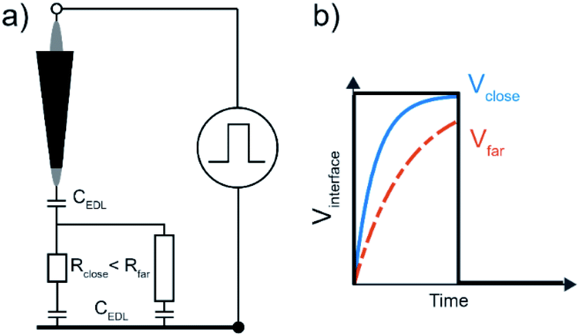 | ||
| Fig. 1 (a) Illustration of the mechanism for electrochemical localization by short voltage pulses. By applying a potential pulse to the probe, the EDL at the substrate will charge more quickly due to the lower path resistance through the solution and associated shorter RC-time. This is illustrated in (b) as the potential of the interface for a short (blue solid line) and long (red dashed line) path, during a potential pulse (black line). | ||
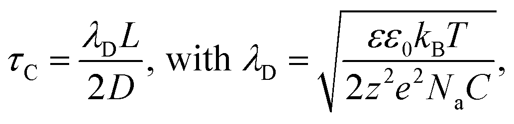
Here, we consider a description of the time constant for interfacial charging analogous to the RC-time to predict the spatial extend of an electrical pulse applied to a scanning electrode. The charging time τC has been identified as the RC time for a simple electrochemical system of two parallel plate, blocking electrodes (i.e. without faradaic current), with a z:z electrolyte (i.e. each ion has equal charge), and an applied step potential, and is given by;33
 | (1) |
In general, the minimum required time (treq) after which an electrochemical reaction can happen upon applying a potential at the electrode is determined by the charging curve of the interface potential (Vinterface, blue dashed curve in Fig. 2a). Here, the interface potential is the electrode potential with respect to the solution potential. Considering the interface as a capacitor, the interface potential rises exponentially with the characteristic τC time 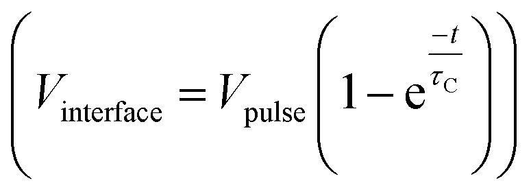 . In other words, τC corresponds to the time required for the interface to charge to ∼63% (i.e. e−1) of the applied potential. In most cases, the voltage-dependent rate of electrochemical reactions is well-described by the Butler–Volmer formalism, where the charge transfer per unit time is proportional to e(Vinterface−Vreq), where Vreq is the minimum thermodynamic potential for the reaction to occur (i.e. redox potential). As such, the minimum charging time (treq) is the time when the interface potential reaches Vreq (leftmost blue dot in Fig. 2a). By defining treq ≡ τCα the required potential and pulse potential are connected by Vreq = Vpulse(1 − e−α) and thus α = Ln(1/(1 − Vreq/Vpulse)) is fully defined by the electrochemical system under consideration and the applied pulse potential.
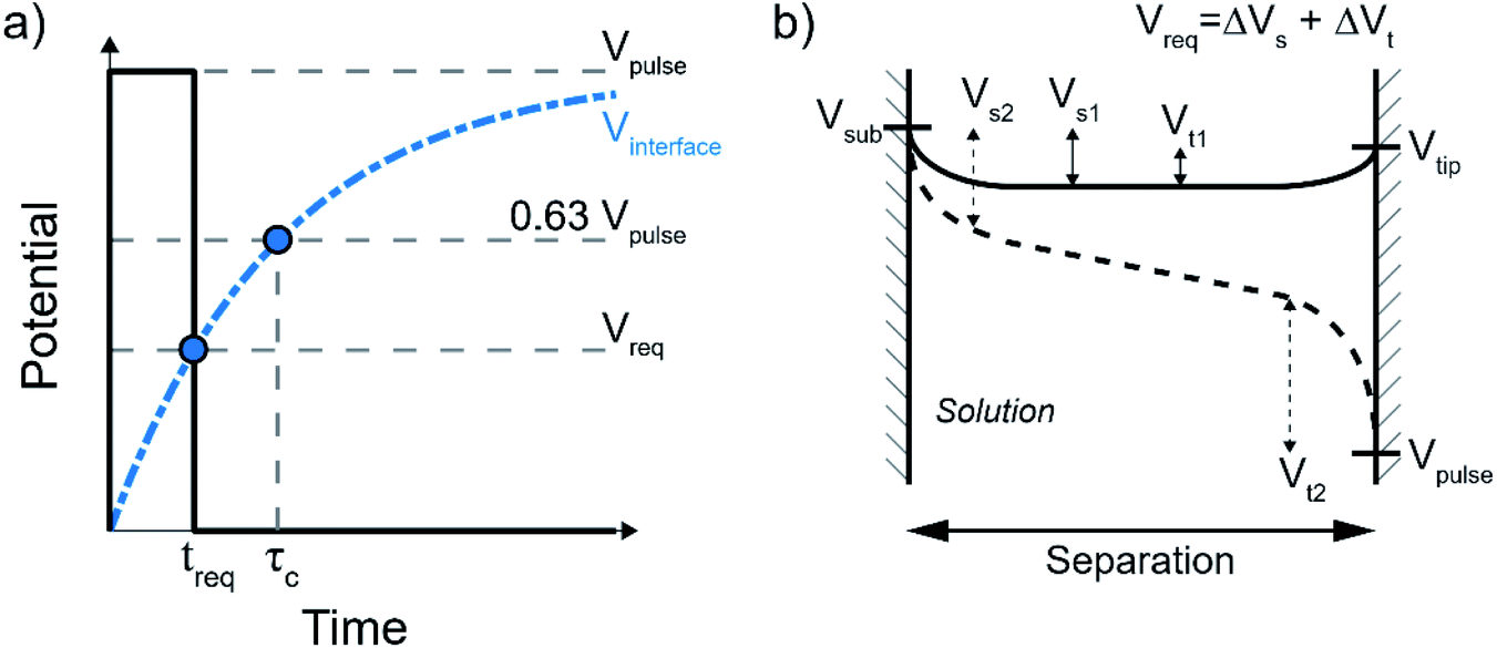 | ||
| Fig. 2 (a) Charging curve of the solid–liquid interface as an ideal capacitor (blue dash-dotted line), defined by the charging time τC. The black solid line represents a potential pulse that is just long enough for the interface to charge to the potential required for the electrochemical reactions. (b) Schematic of the potential landscape in the tip-substrate gap. The solid–liquid potential drop is altered at both the tip and the substrate electrode under influence of the applied pulse, shifting them from their rest potentials with respect to the solution (Vs1 and Vt1) to where the electrochemical reactions are thermodynamically allowed (Vs2 and Vt2). The required potential Vreq is then the sum of the differences Vreq = ΔVs + ΔVt. | ||
In the small tip-substrate gap, the electrochemical system can be defined by two electrodes, the tip and the sample, where a potential pulse at the tip will force a change in the potential drop at the two solid–liquid interfaces. The required potential Vreq to enable local faradaic currents is the change of the two solid–liquid potential drops from their rest potential to the potential of the respective half-reactions. This is illustrated in Fig. 2b, showing the evolution of the potential landscape in the tip-substrate gap that are kept at some rest potential with respect to the solution (Vs1 and Vt1, solid line), as the interfaces are charged to the potential required for the electrochemical reactions (Vs2 and Vt2, dashed line) under influence of a pulse applied to the tip. It is worth noting that these potentials can be reached before the potential in the gap fully equilibrates, as illustrated here by the linear profile in the center.10 The required polarization is then taken as the sum of the potential changes Vreq = ΔVs + ΔVt. It should be noted that the charging dynamics are expected to deviate from the ideal capacitor behavior at potentials above those required for the electrochemical reactions, as the interface may become (increasingly) non-polarizable once charge transfer is allowed. While this picture therefore illustrates the time required to reach sufficient polarization, it does not determine the (faradaic) reaction rates.
Based on this model, the minimum pulse width required to charge the interface sufficiently for a local electrochemical current to occur is then given by α and eqn (1) for a given tip-substrate distance, required potential, and pulse height. For a certain pulse width (tpulse), eqn (1) can be rewritten to obtain the maximum tip-substrate distance at which the substrate is sufficiently charged to enable the electrochemical reaction:
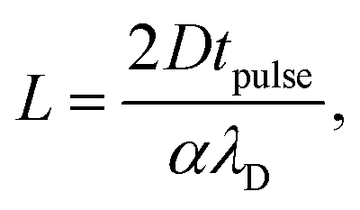 | (2) |
Eqn (2) highlights that the distance of significant charging can be well defined not only through the electrolyte properties (λD and D), but also varied through the experimental parameters Vpulse and Vreq (influenced by the electrochemical system and rest potentials), which influence the minimum charging time through the parameter α. This description can therefore be used to predict the maximum etching distance based directly on the employed electrolyte and the experimental details.
We apply eqn (2) to predict the etching resolution as demonstrated experimentally in previous works of Schuster et al.,12 Kock et al.,11 and De Abril et al.,32 where different metal systems (Cu, Ni), electrolyte concentrations (1–200 mM), pH (1–3), and pulse heights (1.6–3.2 V) are used. Since eqn (2) yields the spatial extent of interface charging sufficient for the etching reaction, and not the rate, these works are considered as they report the achieved resolution for long machining times. These processes are therefore expected to be complete, so that longer machining times will not result in further etching, and the resulting features indicate the maximum spatial extent of the pulse.
The required potential is taken as the sum of the potential changes required for both the probe and the sample, from their rest potentials to the standard potentials of the respective half reactions. As these are etching processes at acidic pH we consider metal oxidation on the substrate and the hydrogen evolution reaction (HER) at the probe, with a pH-dependent potential EHER = 0–60 mV × pH. For the metal oxidation we use ECu = 340 mV, and ENi = 80 mV for copper and nickel, respectively, with potentials relative to the standard hydrogen electrode (SHE). A table of the used parameters can be found in ESI-1.† Importantly, the diffusion coefficient of protons (D = 1 × 10⁻⁸ m2 s−1) is used to determine the time constant in eqn (2), which is typically larger by an order of magnitude compared to values for metal ions in an aqueous solution.
The results are shown in Fig. 3, with symbols indicating the literature values, and the lines the predicted value for L using eqn (2). The legend indicates the electrolyte concentration and etched material. The figure shows that the linear relation between etching resolution (or extent) and the pulse time is captured by our model. Moreover, the predicted etching resolution given by eqn (2) (lines) match the literature closely (within a relative error of ∼50%, ESI-2†), in particular for the shortest pulse times. It is important to note that this implies that the resolution for a given pulse length is limited by the fast diffusion of protons in water-based electrolytes, in line with the sub-ns pulses required for localization of ∼100 nm as reported for electrochemical etching.11 This good agreement for the etching reactions suggests that the diffuse layer description and τC are good indicators to a priori predict the extent of electrochemical reactions in response to a potential pulse at a nearby point-electrode.
 | ||
| Fig. 3 Comparison of the spatial extent of the electrochemical etching reaction reported in literature (symbols), with that predicted by the diffuse layer charge relaxation description using eqn (2) (the matching lines:symbols are dash-dotted:diamonds, solid:squares, long-dash:circles, short-dash:triangle, dash-dot-dot:side-triangle). The results are in good agreement, within a relative error of ∼50% for all datapoints. The legend indicates the electrolyte concentration and etched material. The works considered are references.11,12,32. | ||
Nanoscale charging dynamics for pulsed electrodeposition
While the previously considered works focused on localized etching, we focus now on the local electrodeposition of cobalt with an electrochemical scanning tunneling microscope (EC-STM). We validate the applicability of our model by experimental determination of L (the maximum charging distance) as a function of pulse width for the deposition of Co on Au.In principle, deposition is the reverse process of etching, by inverting the polarity of the pulse. The charging process laid out above is therefore expected to be equivalent, where it should be noted that additional effects such as mass transport limitations or potential barriers for nucleation can affect the growth process. Based on eqn (2), the distance of significant charging, or localization, is proportional to 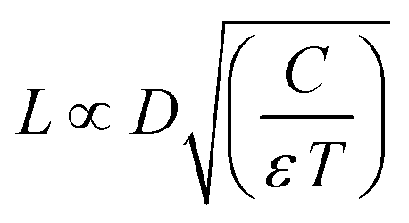 , such that low diffusion coefficients provide the highest resolution. Given the fast diffusion of protons, dimethyl sulfoxide (DMSO) is used as a solvent rather than a water-based electrolyte, similarly to what has been reported previously as a means to increase resolution for the localized etching of gold attributed to the viscosity of the liquid.25,26,35 This is depicted in Fig. 4 showing the distance of significant charging determined for a 50 mM Co salt using eqn (2) when considering either the diffusion coefficient of Co in DMSO (D = 7 × 10⁻¹¹ m2 s−1,36 left), or the diffusion coefficient of protons in water for the same electrolyte (D = 1 × 10⁻⁸ m2 s−1, right). Owing to the different diffusion coefficients of the fastest ionic species in the electrolyte, the distance of relevant charging is two orders of magnitude smaller for Co in DMSO for the same pulse conditions. The distance of significant charging from the tip is directly linked to the localization of the electrochemical reactions and therefore the writing resolution. We therefore consider the absence of protons to be an important factor, where the resolution could be improved by a factor ∼100 based on the difference in diffusion coefficients. As stated above, the figure also highlights that the achievable localization depends on the potential of the pulse with respect to the required potential (Vpulse/Vreq), which determines α in eqn (2). The larger the Vpulse/Vreq ratio, the shorter the pulse width must be to achieve a given desired resolution, which might lead to nonpractical pulse values. It is worth noting that when considering the extent of charging near a scanning probe, reaction profiles can be limited by the tip radius and shape. This is particularly relevant when considering the DMSO solvent in Fig. 4a, yielding values below typical dimensions of the tip (<10 nm). This is an example for Co metal deposition, but can be translated to other material systems that can be electrodeposited, where the resolution can be similarly tailored through the Vpulse/Vreq ratio and pulse width. For practical reasons, an important consideration is the reversibility of the deposition reaction. This requires most careful control of the substrate potential in the case of highly reversible deposition/dissolution, to prevent global deposition on the substrate to occur, while also preventing dissolution after deposition.26 For the validity of eqn (2) it is worth realizing that the described model relies on a capacitance of the interface based on the Gouy–Chapman model,33 which is known to not always be valid in e.g. cases such as high potentials.29 Further, effects related to e.g. mass transport and nucleation are not captured.
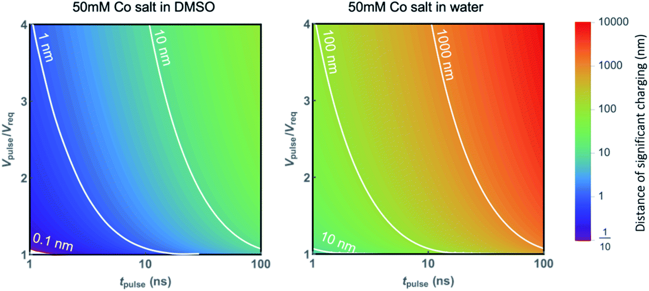 | ||
| Fig. 4 Contour plot of the maximum distance between 2 electrodes where electrochemical reactions are allowed due to significant charging, using eqn (2) as a function of pulse width and pulse height normalized to the required potential (determining α). Diffusion coefficients of 7 × 10⁻¹¹ m2 s−1 and 1 × 10⁻⁸ m2 s−1 are used for Co in DMSO (left) and protons in water (right), respectively, with εDMSO = 46.7 and εwater = 80.1. | ||
The setup used for deposition was as follows. The STM tip was coupled to a bipotentiostat in a 4-electrode setup and could be switched to a pulse generator by means of a relay, as is shown schematically in Fig. 5a, and described in detail in the Methods and ESI-3.† Importantly, to ensure that current flows between the tip and the sample a home-built low-pass filter was included to the potentiostat feedback loop, to prevent the counter electrode from counteracting the applied pulse. The electrochemical cell consisted of a Au(111) single crystal substrate with two gold wires for both the counter electrode and as a quasi-reference electrode (QRE). The STM tips were either Pt or Pt–Ir, and were coated with an insulating wax to decrease the exposed area and minimize parasitic faradaic current along the length of the probe. All experiments were done in ambient conditions. Fig. 5b shows a cyclic voltammogram (CV) of the Au substrate in 500 mM CoSO4 in DMSO (blue curve). The reduction reaction with an onset at ∼−900 mV is associated with the deposition of cobalt, as confirmed by in situ STM imaging (not shown). The cobalt dissolution is connected to the oxidation wave starting at ∼−400 mV, confirmed by the absence of this wave when stopping the scan at cathodic potentials >−900 mV (grey dashed curve). Importantly the reduction/oxidation of cobalt are separated in potential by a few hundred mV, which provides an electrochemical window where the substrate potential can be fixed to prevent global deposition on the substrate, and dissolution of the deposited structures.
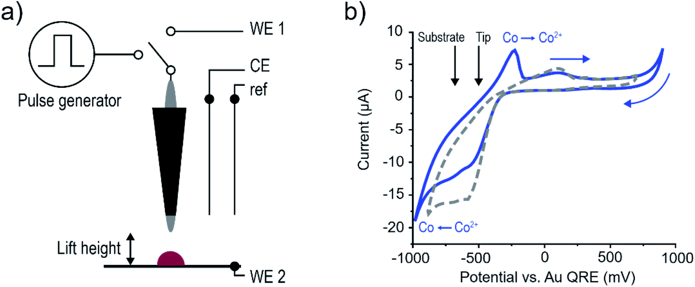 | ||
| Fig. 5 (a) Schematic representation of the EC-STM setup, in a 4-electrode configuration. Local deposition is induced by voltage pulses applied to the tip, after lifting the tip by a distance lift height and changing its electronic connection from the bipotentiostat (WE 1) to an external pulse generator. (b) Cyclic voltammogram on the Au (111) single crystal substrate in 500 mM CoSO4 (DMSO), at a scan rate of 100 mV s−1. The reduction (∼−900 mV) and oxidation (∼−400 mV) potentials for Co2+/Co are indicated (blue curve), and are not present when reversing the scan at lower cathodic potentials (grey dashed curve). Typical tip and substrate rest potentials are indicated by the black arrows. Note that they are separated by 200 mV to enable tunnelling feedback when scanning. | ||
To find the maximum distance L from the tip where deposition occurs for a certain pulse width in the DMSO electrolyte, the following experiment is conducted (Fig. 6a, and ESI-4†). (i) Deposition is attempted by first lifting the tip by a certain height and then sending a pulse train with a pulse width (tpulse) and a period of 10 μs (104 pulses, ON value 2.5 V, OFF value 0 V). This is repeated for ten locations spaced 50 nm apart in a single line (where the tip is approached to the surfaces for each point before lifting), (ii) the surface topography is scanned to check for deposition and in the absence of deposition the process is repeated with increasing pulse ON time (tpulse) until deposition is observed (ESI-5†), (iii) the process is repeated at an increased lift height. The routine then gives the minimum pulse width required to initiate deposition for a certain lift height, or inversely, the maximum distance L over which sufficient charging for deposition occurs for a certain pulse width. The determination of L is thus reduced to a binary qualification of the presence or absence of deposition, rather than attempting to determine the maximum distance from the width of a deposit.
In principle, this protocol is designed to reduce the experiment dimensionality to 1D, as it only considers the shortest path from apex of the tip to the sample no matter the tip shape, rather than considering the lateral extent of the growth. The use of such a protocol is supported by the fact that we often observed deposits much wider than the lift height despite not observing any deposition at slightly smaller pulse widths, as shown in ESI-5† for all datapoints. Sweeping the lift height is done at the same spot on the substrate, with the substrate electrochemically cleaned between experiments through lifting of the substrate potential above the cobalt oxidation potential. In all cases lifting the potential resulted in the deposits dissolving, indirectly confirming that they consist of cobalt (ESI-5†).
Fig. 6b shows the shortest pulse width for which deposition occurred for a certain lift height. The error bars indicate the longest pulse for which no deposition was observed (10 ns for the orange circles), and the dashed lines are linear fits to the data, illustrating the linear dependence on pulse time as predicted by the model. The different symbols indicate sequences done with different STM tips, with scanning electron microscope (SEM) images of the tips provided in ESI-6.† The experiments were done in a 50 mM CoSO4 (DMSO) solution (which is one order of magnitude lower than that used for the CV in Fig. 4). The substrate rest potential was empirically chosen to be right before cobalt deposition was observed with the STM (−700/−900 mV (circles, squares), and −850 mV/−1050 mV (diamonds) vs. Au QRE, respectively.). The tip rest potential was set 200 mV positive to that of the substrate to enable imaging. Given that the substrate is already almost at the required potential for cobalt reduction and that the potential difference between cobalt reduction and DMSO oxidation is found to be ∼1.7 V, we estimate a required potential of 1.5 V for the tip.
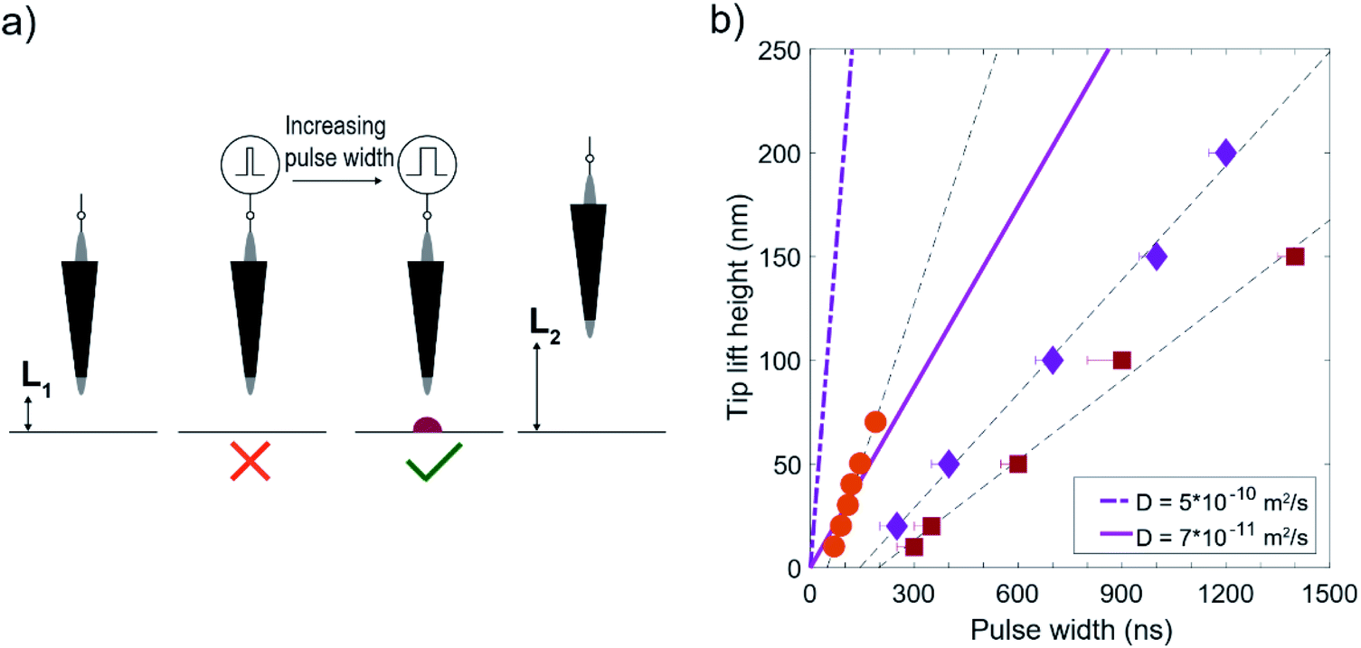 | ||
| Fig. 6 (a) Illustration of the deposition protocol to determine the maximum distance over which deposition occurs. Deposition is attempted at a certain distance L1 by increasing the pulse width until deposition is observed. The surface is scanned after every pulse sequence with a given pulse width. Once deposition is observed, the sequence is repeated at a larger distance (L2) (b) tip lift height vs. pulse width, obtained with the procedure illustrated in (a). The datapoints indicate the minimum pulse width at which deposition is observed, with error bars indicating the longest pulse without deposition and the dashed lines being linear fits to the data. The different symbols indicate different STM tips (shown in ESI-6†). The bold lines (solid, dash-dotted) represent the expected distance from eqn (2), for the employed experimental parameters (see main text). | ||
The bold lines (solid and dash-dotted) correspond to the values predicted by eqn (2), where α is ∼0.92 for Vpulse = 2.5 V and Vreq = 1.5 V based on the separation of the main reduction and oxidation features in the CV in Fig. 5b, and using εDMSO = 46.7 to obtain λD. Curves are shown for both a diffusion coefficient of cobalt in DMSO of 5 × 10⁻¹⁰ m2 s−1, based on measurements of CoCl2 in water37 and scaled with the viscosity η of DMSO (ηwater![[thin space (1/6-em)]](https://www.rsc.org/images/entities/char_2009.gif) :ηDMSO = 1:2, with D ∝ 1/η using Walden's rule), and for D = 7 × 10⁻¹¹ m2 s−1, found in literature.36 The difference between those values is expected to be due to the solvation of cobalt ions with either water or DMSO. As our experiments are carried out under ambient conditions, and the DMSO is hygroscopic, the actual diffusion coefficient is expected to be in between these values depending on the cobalt solvation.35
:ηDMSO = 1:2, with D ∝ 1/η using Walden's rule), and for D = 7 × 10⁻¹¹ m2 s−1, found in literature.36 The difference between those values is expected to be due to the solvation of cobalt ions with either water or DMSO. As our experiments are carried out under ambient conditions, and the DMSO is hygroscopic, the actual diffusion coefficient is expected to be in between these values depending on the cobalt solvation.35
From the figure it can be seen that the distance over which deposition occurs increases linearly with the pulse width, as expected from eqn (2). It is worth mentioning that we observed deposition in aqueous electrolytes (50 mM CoSO4 (aq), pH ∼4) for 10 and 20 ns pulses at lift heights of 200 and 500 nm respectively, with otherwise unchanged experimental conditions (ESI-7†). As such, the potential pulse is much more confined in the DMSO electrolyte (∼60×), in line with the expectation from the diffuse layer charging description.
Despite the qualitative agreement between the different datasets and the model, the local charging appears to require longer times than the model predictions from eqn (2). It is worth mentioning that the experiments were executed using the same stock solution in the chronology of decreasing slope (circles, diamonds, squares), which could indicate some effect of aging of the electrolyte. From the model perspective, such deviation can be either due to an increased α due to an underestimated required potential, or non-ideal charging. The latter can potentially be due to parasitic capacitance of the STM tip, as the different datasets were performed with different STM tips. It should be stressed that the model considers 1D charging and an instantaneously applied potential between the 2 electrodes. Parasitic charging along the STM tip might therefore perturb the pulse arriving at the apex, which we cannot measure in our experimental setup. In fact, it has been demonstrated recently that the machining resolution of a pulsed etching process can be improved for a given pulse length by introducing an additional capacitor that slows down the charging,38 further suggesting that pulse deformation at the tip may be responsible for the discrepancy between the model and experiments. Compared to the etching experiments considered in Fig. 3, differences for the deposition considered here might further arise due to effects related to mass transport and nucleation. Strikingly, we also observe that the linear fits to the three datasets are offset with respect to the x-axis, and intercept the y-axis at the same point, −25 nm ± 1 nm. As this offset is in the order of the expected tip radius (Rtip) this is reminiscent of the theory used to describe tunnelling in a STM, where a spherically symmetric tip is effectively equivalent to a point located at distance Rtip from the apex.39
Direct electrochemical writing of cobalt nanostructures
Finally, we demonstrate the possibility of nanoscale writing using this method. Fig. 6a displays the height profiles of lines written at different lift heights of the tip. The lines are 500 nm in length, and are written with 10 consecutive pulse sequences positioned 50 nm apart, as indicated by the red dots in the first panel. At every point the tip is approached to the surface and is then retracted by a certain lift height after which a pulse train is sent. For the lines in Fig. 6a the pulse train consists of 2000, 5 V pulses of 100 ns, with a 10 μs period. The experiments were done in a 500 mM CoSO4 (DMSO) solution. The tip/sample potentials are kept at −500/−700 mV vs. Au QRE. Additionally, the low level (OFF value) of the pulse to the tip is set to 1 V to reduce the total required charging time. Again, dissolution of written lines by raising the substrate potential was confirmed (not shown). From the STM images, a writing linewidth of ∼50 nm is observed (full width at half maximum, FWHM). Fig. 7b and c illustrate the robustness of the localization by considering the distance Lmax from the edge of the line profile to the tip position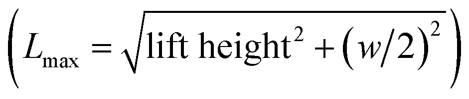 , with w taken as the width of the deposit higher than 1 nm. This maximum lateral charging distance is found to be constant at ∼55 nm, which agrees with the absence of deposition at a lift height of 60 nm and highlights the applicability of the mechanism for in-plane lateral growth. The shape of the lines changes as a function of the lift height however, as illustrated by the FWHM in Fig. 7d. In fact, the aspect ratio of the line can be modulated further by varying the number of pulses (ESI-8†). It should be noted that in this case significant charging up to ∼800 nm from the probe is expected from eqn (2) (using D = 7 × 10⁻¹¹) due to the high applied potential and consequently low value of α. Charging therefore appears to be slowed down significantly compared to the prediction, which could be related to breaking down of the underlying Gouy–Chapman model assumptions at these applied potentials.29
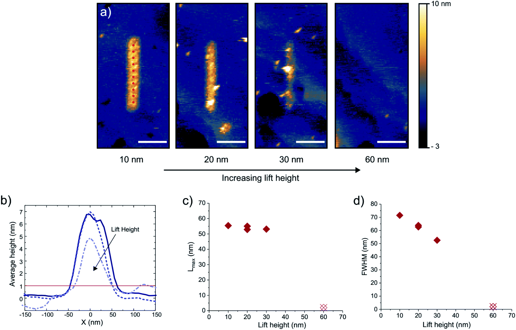 | ||
| Fig. 7 (a) STM topography images of lines written at different lift heights by 10 consecutive pulse sequences, spaced 50 nm apart (red dots in first panel). The scale bars are 200 nm. (b) Profile averaged along the length of the lines in (a) for different lift heights (solid, 10 nm, dashed, 20 nm, dash-dotted 30 nm, the arrow indicating increasing lift height). The width of the lines to compute Lmax is taken as the width above 1 nm (red line). (c) Lmax as defined in the text as the shortest path from the tip to the edge of the deposit for different lift heights. (d) Full width at half maximum (FWHM) of the lines as a function of lift height. | ||
Conclusions
In conclusion, we use the framework of diffuse layer charging to describe the localization of electrical double layer charging in response to a potential pulse applied to a probe, for the purpose of confined electrochemistry. The resolution for electrochemical etching demonstrated in the literature is found to be accurately described in terms of fundamental constants of the electrolyte, using this diffuse layer time constant. The presented model therefore provides a means to predict the extent of the electrochemical reaction a priori in terms of the experimental parameters. A relevant consequence is that the use of aqueous electrolytes could be detrimental to the achievable resolution due to the high diffusion coefficient of protons, therefore requiring extremely short pulses as observed in literature for electrochemical etching. This concept is applied for the inverse process of local electrodeposition through decreasing the extent of significant double layer charging by using DMSO as a solvent to achieve a slower diffusion of ions in solution, due to the absence of protons. In accordance with literature we demonstrate that this drastically improves the localization of the pulse compared to aqueous solutions (∼60×). Finally, we show that pulsed deposition can be used for direct-write patterning purposes, achieving a linewidth of cobalt lines of ∼50 nm, which can potentially be reduced further by optimizing experimental parameters such as the employed pulse (pulse height and rest potentials), solvent, and the radius of the tip. While the present demonstration is limited to mainly in-plane writing, the changing aspect ratio of the structure at larger pulse numbers suggests that this could be expanded to further growth in the out of plane direction. This framework is expected to be general and, as highlighted in Fig. 4, can be used to predict the resolution for the electrochemical etching and writing of other materials. An important consideration is the reversibility of the deposition reaction however, requiring most careful control of the substrate potential in the case of highly reversible deposition/dissolution. Examples of such potential material systems for local SPM deposition could be metals such as Al,40 or even semiconductors like PbO2.41 More broadly, this framework can be used to predict the spatial extent of pulsed potential techniques applied to an electrochemical scanning probe.Methods
Solution preparation
Solutions were prepared in glass vials cleaned in acid piranha and washed with MilliQ® water. Solutions were prepared with CoSO4·7H2O powder (99.999%, Alfa Aesar, Germany) in dimethyl sulfoxide (DMSO, analytical reagent grade, Fisher Scientific UK).Tip preparation
PtIr STM tips were purchased from NaugaNeedles (NN-USPtIr-WR250, nominal radius 25–50 nm). An electrochemically etched Pt wire tip was used for the orange circle datapoints in Fig. 6. All tips were coated by pulling them through a heated thermoplastic wax (Apiezon, wax W).Electrochemical setup
The electrochemical cell was made from polychlorotrifluorethylene. The sample was Au single crystal ((111)-out-of-plane < 1%, 99.999% purity, Mateck, Germany). For the experiments in Fig. 6 (diamonds, squares) the sample was cleaned by cyclic voltammetry in water with low amounts of sulfuric acid (H2SO4) prior to the deposition sequence.Electrochemical pulsed STM electronics
Measurements were conducted with an STM (Cypher-AFM in STM-mode, Asylum Research, USA). Potentials were controlled with a bipotentiostat (PGUmicro, IPS, Germany), and pulses were supplied by an external pulse generator (2 × 81111A, Agilent, USA). Lifting the tip for deposition experiments was done through a closed loop piezo controlled z-motor. A detailed description of the setup can be found in ESI-3.†Author contributions
AR designed and built the STM-based deposition setup, wrote the control software, established and verified general experimental procedures, introduced MA to the setup and advised his experimental work. RS supervised AR's contribution to the work. MA conducted the deposition experiments. MA and EAL devised the experiments and analyzed the results. MA drafted the manuscript under supervision of EAL. All authors discussed the results and reviewed and commented on the manuscript.Conflicts of interest
There are no conflicts to declare.Acknowledgements
This work is part of the research program at the Netherlands Organisation for Scientific Research (NWO). AR was supported from ETH Zürich through grant no. ETH 47 14-2. Electron-microscopy analysis was performed at ScopeM, the microscopy platform of ETH Zürich. A. R. would like to thank Prof. Dr Rolf Schuster (Karlsruhe Institute of Technology) for his input and advice for the construction of the setup, and Martin Elsener (ETH Zürich) for machining setup components. MA and EAL also thank Prof. Dr Joost Frenken for discussions on the electrochemical STM, and D. Ursem for etching the used Pt tips.Notes and references
- G. Gonella, et al., Water at charged interfaces, Nat. Rev. Chem., 2021, 5, 466–485 CrossRef CAS.
- S. Sarkar, S. C. S. Lai and S. G. Lemay, Unconventional electrochemistry in micro-/nanofluidic systems, Micromachines, 2016, 7, 81 CrossRef PubMed.
- M. H. Futscher, et al., Quantification of ion migration in CH 3 NH 3 PbI 3 perovskite solar cells by transient capacitance measurements, Mater. Horiz., 2019, 6, 1497–1503 RSC.
- M. Janssen, E. Griffioen, P. M. Biesheuvel, R. V. Roij and B. Erné, Coulometry and Calorimetry of Electric Double Layer Formation in Porous Electrodes, Phys. Rev. Lett., 2017, 1–5, 166002 CrossRef PubMed.
- D. Toth, et al., Nanoscale Charge Accumulation and Its Effect on Carrier Dynamics in Tri-cation Perovskite Structures, ACS Appl. Mater. Interfaces, 2020, 12, 48057–48066 CrossRef CAS PubMed.
- L. Guo, G. Oskam, A. Radisic, P. M. Hoffmann and P. C. Searson, Island growth in electrodeposition, J. Phys. D: Appl. Phys., 2011, 44, 443001 CrossRef.
- R. Tivony, S. Safran, P. Pincus, G. Silbert and J. Klein, Charging dynamics of an individual nanopore, Nat. Commun., 2018, 9, 1–8 CrossRef CAS PubMed.
- L. Collins, J. I. Kilpatrick, S. V. Kalinin and B. J. Rodriguez, Towards nanoscale electrical measurements in liquid by advanced KPFM techniques: a review, Rep. Prog. Phys., 2018, 81, 086101 CrossRef PubMed.
- K. Hirata, et al., Visualizing charges accumulated in an electric double layer by three-dimensional open-loop electric potential microscopy, Nanoscale, 2018, 10, 14736–14746 RSC.
- L. Collins, et al., Probing charge screening dynamics and electrochemical processes at the solid–liquid interface with electrochemical force microscopy, Nat. Commun., 2014, 5, 3871 CrossRef CAS PubMed.
- M. Kock, V. Kirchner and R. Schuster, Electrochemical micromachining with ultrashort voltage pulses–a versatile method with lithographical precision, Electrochim. Acta, 2003, 48, 3213–3219 CrossRef CAS.
- R. Schuster, V. Kirchner, P. Allongue and G. Ertl, Electrochemical Micromachining, Science, 2000, 289, 98–101 CrossRef CAS PubMed.
- R. Schuster, V. Kirchner, X. H. Xia, A. M. Bittner and G. Ertl, Nanoscale electrochemistry, Phys. Rev. Lett., 1998, 80, 5599–5602 CrossRef CAS.
- D. M. Kolb, Nanofabrication of Small Copper Clusters on Gold(111) Electrodes by a Scanning Tunneling Microscope, Science, 1997, 275, 1097–1099 CrossRef CAS PubMed.
- W. Schindler, D. Hofmann and J. Kirschner, Localized Electrodeposition Using a Scanning Tunneling Microscope Tip as a Nanoelectrode, J. Electrochem. Soc., 2001, 148, C124 CrossRef CAS.
- R. T. Pötzschke, G. Staikov, W. J. Lorenz and W. Wiesbeck, Electrochemical Nanostructuring of n-Si(111) Single-Crystal Faces, J. Electrochem. Soc., 1999, 146, 141 CrossRef.
- R. Widmer and H. Siegenthaler, Nanostructuring experiments in the system Ag(111)/Pb2+, Electrochem. Commun., 2005, 7, 421–426 CrossRef CAS.
- A. Reiser, et al., Multi-metal electrohydrodynamic redox 3D printing at the submicron scale, Nat. Commun., 2019, 10, 1853 CrossRef PubMed.
- L. Hirt, et al., Template-Free 3D Microprinting of Metals Using a Force-Controlled Nanopipette for Layer-by-Layer Electrodeposition, Adv. Mater., 2016, 28, 2311–2315 CrossRef CAS PubMed.
- D. Momotenko, A. Page, M. Adobes-Vidal and P. R. Unwin, Write–Read 3D Patterning with a Dual-Channel Nanopipette, ACS Nano, 2016, 10, 8871–8878 CrossRef CAS PubMed.
- A. P. Suryavanshi and M.-F. Yu, Electrochemical fountain pen nanofabrication of vertically grown platinum nanowires, Nanotechnology, 2007, 18, 105305 CrossRef.
- J. Hu and M.-F. Yu, Meniscus-Confined Three-Dimensional Electrodeposition for Direct Writing of Wire Bonds, Science, 2010, 329, 313–316 CrossRef CAS PubMed.
- L. Hirt, A. Reiser, R. Spolenak and T. Zambelli, Additive Manufacturing of Metal Structures at the Micrometer Scale, Adv. Mater., 2017, 29, 1604211 CrossRef PubMed.
- D. Zhan, et al., Electrochemical micro/nano-machining: principles and practices, Chem. Soc. Rev., 2017, 46, 1526–1544 RSC.
- E. M. Moustafa, O. Mann, W. Furbeth and R. Schuster, Electrochemical Behaviour of Iron in a Third-Generation Ionic Liquid: Cyclic Voltammetry and Micromachining Investigations, ChemPhysChem, 2009, 10, 3090–3096 CrossRef CAS PubMed.
- X. Ma, A. Bán and R. Schuster, Electrochemical machining of gold microstructures in LiCl/dimethyl sulfoxide, ChemPhysChem, 2010, 11, 616–621 CrossRef CAS PubMed.
- A. M. Smith, A. A. Lee and S. Perkin, The Electrostatic Screening Length in Concentrated Electrolytes Increases with Concentration, J. Phys. Chem. Lett., 2016, 7, 2157–2163 CrossRef CAS PubMed.
- M. Khademi and D. P. J. Barz, Structure of the Electrical Double Layer Revisited: Electrode Capacitance in Aqueous Solutions, Langmuir, 2020, 36, 4250–4260 CrossRef CAS PubMed.
- M. Z. Bazant, M. Sabri Kilic, B. D. Storey and A. Ajdari, Nonlinear electrokinetics at large voltages, New J. Phys., 2009, 11, 075016 CrossRef.
- Z. Shi and J. Lipkowski, Chloride adsorption at the Au(111) electrode surface, J. Electroanal. Chem., 1996, 403, 225–239 CrossRef.
- Z. Kerner and T. Pajkossy, On the origin of capacitance dispersion of rough electrodes, Electrochim. Acta, 2000, 46, 207–211 CrossRef CAS.
- O. de Abril, A. Gündel, F. Maroun, P. Allongue and R. Schuster, Single-step electrochemical nanolithography of metal thin films by localized etching with an AFM tip, Nanotechnology, 2008, 19, 325301 CrossRef CAS PubMed.
- M. Z. Bazant, K. Thornton and A. Ajdari, Diffuse-charge dynamics in electrochemical systems, Phys. Rev. E, 2004, 70, 021506 CrossRef PubMed.
- J. A. Kenney, G. S. Hwang and W. Shin, Two-dimensional computational model for electrochemical micromachining with ultrashort voltage pulses, Appl. Phys. Lett., 2004, 84, 3774–3776 CrossRef CAS.
- X. Ma and R. Schuster, Locally enhanced cathodoluminescence of electrochemically fabricated gold nanostructures, J. Electroanal. Chem., 2011, 662, 12–16 CrossRef CAS.
- J. N. Butler, Electrochemistry in dimethyl sulfoxide, J. Electroanal. Chem. Interfacial Electrochem., 1967, 14, 89–116 CrossRef CAS.
- A. C. F. Ribeiro, V. M. M. Lobo and J. J. S. Natividade, Diffusion Coefficients in Aqueous Solutions of Cobalt Chloride at 298.15 K, J. Chem. Eng. Data, 2002, 47, 539–541 CrossRef CAS.
- C. Zhao, X. Bai and L. Xu, Controlled Electrochemical Nanomachining with Adjustable Capacitance, J. Electrochem. Soc., 2018, 165, E269–E273 CrossRef CAS.
- J. Tersoff and D. R. Hamann, Theory of the scanning tunneling microscope, Phys. Rev. B: Condens. Matter Mater. Phys., 1985, 31, 805–813 CrossRef CAS PubMed.
- L. Legrand, A. Tranchant and R. Messina, Electrodeposition Studies of Aluminum on Tungsten Electrode from DMSO 2 Electrolytes: Determination of AlIII Species Diffusion Coefficients, J. Electrochem. Soc., 1994, 141, 378–382 CrossRef CAS.
- A. B. Velichenko, D. V. Girenko and F. I. Danilov, Electrodeposition of lead dioxide at an Au electrode, Electrochim. Acta, 1995, 40, 2803–2807 CrossRef CAS.
Footnote |
| † Electronic supplementary information (ESI) available. See DOI: 10.1039/d1na00779c |
| This journal is © The Royal Society of Chemistry 2022 |