
 Open Access Article
 This Open Access Article is licensed under a Creative Commons Attribution-Non Commercial 3.0 Unported Licence
Utilising problematic waste to detect toxic gas release in the environment: fabricating a NiO doped CuO nanoflake based ammonia sensor from e-waste†
Rumana
Hossain‡
 *,
Kamrul
Hassan‡
and
Veena
Sahajwalla
*,
Kamrul
Hassan‡
and
Veena
Sahajwalla
Centre for Sustainable Materials Research and Technology, SMaRT@UNSW, School of Materials Science and Engineering, UNSW, Sydney, Australia. E-mail: r.hossain@unsw.edu.au
First published on 11th July 2022
Abstract
Using problematic electronic waste to synthesise high-purity nanomaterials can enable sustainable production and create opportunities to divert waste from landfills. Reported here is a simple strategy for the controllable synthesis of in situ NiO doped CuO nanoflakes from waste flexible printed circuit boards (FPCBs) using a chemothermal microrecycling process, and the nanomaterial is then utilised for an ammonia (NH3) sensor at room temperature. Characterisation of the nanoflakes confirmed the purity of the CuO phase with a monoclinic structure without the formation of the Cu2O phase. The NiO doped CuO 2D nanoflakes made of an assembly of 1D nanorods with a high surface area of 115.703 m2 g−1 are selectively synthesised from the waste FPCBs and have outstanding gas sensing characteristics such as a high response, a fast response (11.7 s) and a recovery time of (21.5 s), good stability, and superior selectivity towards 200 ppm of NH3 gas at room temperature (RT, 20 °C). From a broader perspective, the process opens up exciting new avenues explore the production of toxic gas sensing functional materials from toxic and problematic waste.
Introduction
As natural resources decline, global industrial solutions and manufacturing processes must embrace novel strategies which replace conventional resources with materials reformed from waste. One of the most problematic waste streams, electronic waste (e-waste), which made up of many valuable metals and non-metals.1,2 For example, flexible printed circuit boards (FPCBs) contain more than 99% pure copper (Cu) embedded in non-metals including polyimide (PI) and resin2,3. The Ni-based emulsions are widely used as a surface finish for FPCBs, especially to protect against oxidation at the soldering sites. Electronic devices come in many different shapes and sizes. Therefore, FPCBs are made as a large sheet and then punched and cut into the desired shape in the final stage of production, leaving behind a large amount of waste rich in valuable copper metal.2,4 This copper could be recovered using a thermal disengagement technique (TDT)5,6 and then used for other industrial applications. In this study, we have used copper recovered from FPCB waste to synthesise a CuO nanomaterial.Researchers have suggested various methods for the preparation of ultra-fine copper powders from waste printed circuit boards.7,8 These methods include chemical reduction, cementation,9 electrochemical processes,10,11 and electrokinetic processes.12 In the suggested processes, copper was leached in the first step, and nanomaterials were prepared in the second step. The nanostructured CuO is especially versatile and provides unique characteristics for many applications, including sensors,13 high-critical-temperature semiconductors,14 lithium-ion batteries,15 field emission emitters,16 and catalysts.17
Metal oxide-based ammonia sensors have a huge attraction because of their low-cost fabrication and sensor responsivity to the exposures, however, it also has a few disadvantages such as a higher operating temperature, a short life, and poor selectivity. Many industries use coolants during the processes used to manufacture chemicals, automobiles, food, textile, paper, and fertilizers, and these coolants pollute the environment by releasing toxic NH3 during the cooling process in the form of aerosols and smog.18 The NH3 is highly toxic and flammable at a concentration level of 16–28% volume in air, being a fire hazard and it will also produce toxic gases.19 Exposure to NH3 for a period can result in lung disease, blindness, or death, and indications of exposure present as eye irritation, burning of the nose, throat, and respiratory tract.20,21 A threshold limit of 50 ppm ammonia exposure is regulated and commissioned by the Occupational Safety and Health Administration (OSHA).22 As per the regulation, an industry with NH3 exposures must have a high-quality NH3 sensor for safety, process control, and detection for controlling environmental exposure and pollution. This demands a high-quality sensor for detecting the NH3 leakage into the environment. A few researchers have fabricated sensors for RT sensing of NH3 including organic diodes,23 polyaniline-based polymers24 or PEDOT![[thin space (1/6-em)]](https://www.rsc.org/images/entities/char_2009.gif) :PSS nanowires,25 porous SiC ammonia sensor,26 surface-ruthenated zinc oxide,27 acrylic acid doped polyaniline (PANI:AA).28 In this study, copper was recovered using a TDT, and in situ NiO-doped CuO nanoflakes were produced via a wet chemical route, and the synthesised nanoflakes were evaluated for their suitability for NH3 gas detection at RT.
:PSS nanowires,25 porous SiC ammonia sensor,26 surface-ruthenated zinc oxide,27 acrylic acid doped polyaniline (PANI:AA).28 In this study, copper was recovered using a TDT, and in situ NiO-doped CuO nanoflakes were produced via a wet chemical route, and the synthesised nanoflakes were evaluated for their suitability for NH3 gas detection at RT.
A novel fabrication process is developed to obtain a highly porous and nanostructured NiO doped CuO capable of a rapid response property at RT, improvised sensitivity of NH3, and high relative humidity (RH). The selectivity of NH3 is examined and evaluated by comparing the NH3 with ethanol, acetone, methane, hydrogen, isoprene, methanol, formaldehyde, CO, and acetic acid. Furthermore, the sensing mechanism for the detection of NH3 is also discussed.
In this research, a controllable and simple synthesis of in situ NiO doped CuO nanoflakes from waste FPCBs using a chemothermal microrecycling process has been conducted, and the nanomaterial was utilised for in a NH3 sensor at RT. For the first time, the FPCBs were utilised to synthesise in situ NiO doped CuO nanoflakes to fabricate NH3 sensors. Most of the previously fabricated CuO-based sensors were made from virgin sources. Previously, researchers have utilised the conventional printed circuit board (PCB) waste source to synthesise CuO nanomaterials which are associated with multimaterials such as glass fibers, ceramic materials, and other metals such as Pd, Sn, Zn, and so on.3 The conventional system needs several steps to synthesise high purity nanomaterials. In this study, for the first time, FPCB waste was utilised. The FPCBs are made as a large sheet and then punched and cut into the desired shape in the final stage of production, leaving behind a large amount of waste rich in valuable copper metal (more than 99% pure). As this is primary waste it does not need to be dismantled from the waste electronic device which made the process less complicated and more efficient.2 Ni-based emulsions are used as a surface finish for FPCBs, especially to protect against oxidation at soldering sites which is the source of the NiO doping in CuO nanomaterials.2 To synthesise NiO doped nanomaterials, previous researchers used pure NiCO3, Ni(NO3)2, and NiSO4, whereas in this research no extra raw materials were used for this purpose.29–33 An additional doping agent for NiO doping was not used in this research which has made the process cost-effective. For the first time, waste FPCBs were utilised to produce NH3 sensors. In this study, the bandgap energy for CuO was measured as 1.6 eV, which was higher than the value for bulk CuO (1.2 eV)34,35 and lower than the values for the NiO nanoparticles (3.8 eV).36,37 Incorporating a small amount of NiO with CuO can shift the bandgap to a higher region compared to that of the pure CuO.38,39 The actual bandgap of the bulk CuO was 1.2 eV, which has been considered as low and the bandgap of NiO was 3.8 eV which has been considered as high for use in sensor applications. The synthesised CuO nanoflakes exhibited a bandgap of 1.6 eV due to the incorporation of a small amount of NiO in situ, making it a good candidate for the sensing application.
The sources and the composition of this waste are consistent, because it was provided by one of the leading manufacturers who produce several hundreds of kilograms of this waste every week in their industry in Thailand, and they have their manufacturing industries in other places of the world (the amount of the waste and the name of the industry is not disclosed for ethical reasons). The high-yield, highly selective separation methodology developed for detecting the toxic gas by utilising toxic e-waste, has the potential to reduce the amount of waste produced by the widespread industrialisation of electronic devices, and to recover valuable materials which could reduce the demand for dwindling natural resources.
Experimental methods
Materials
The multilayer waste FPCBs used in this research were supplied by local recyclers in Sydney, Australia. The shredded FPCBs were first processed using a TDT5,6 at 600 °C for 20 min. In this process, the polymeric layer was thermally disengaged, and pure Cu foils were recovered and further processed via a chemical route. To chemically synthesise CuO from the recovered Cu foils with a carbon (C) residue, this study used HNO3, H2SO4, and NaOH.Synthesis of the CuO nanoflakes from the recovered Cu foils
The chemical synthesis of CuO began with the recovered Cu and C mixture. The Cu and C mixture (6 mg) was immersed in an acidic solution (3 mL of 70% HNO3 and 5 mL of 98% H2SO4), where the C particles floated, and the Cu dissolved and became a blue solution. The digestion of Cu in acidic media can be explained by the following rection:| 3Cu + 3H2SO4 + 2HNO3 → 3CuSO4 + 2NO + 4H2O | (1) |
The blue solution was composed of CuSO4. The residual solid C was filtered out and the clean CuSO4 was stored for the next step. To convert the CuSO4 into CuO, a NaOH solution was added to the blue solution. During the addition of the NaOH, the solution became an aqua color. Once 15 mL of 50% NaOH was added to the solution and then heated on a hot plate at 100 °C, the color turned black from the CuO residues. The reaction order is as follows:
| CuSO4 + 2NaOH → Cu(OH)2 + Na2SO4 | (2) |
Upon being heated the solution turned into black CuO:
| Cu(OH)2 + heat → CuO + H2O | (3) |
The black residue in the solution was filtered and the black powder was oven-dried by heating at 80 °C overnight.
Materials characterisation methods
Thermogravimetric (TGA) analysis using an STA 8000 (PerkinElmer) was performed to identify the thermal behaviour of the FPCB. Using inductively-coupled plasma optical emission spectroscopy (ICP-OES) with an Optima 7300 (PerkinElmer) the elements in the materials were identified, after digestion of the product. The recovered copper was also analysed using laser-induced breakdown spectroscopy (LIBS). The phase and elemental composition were confirmed with a X'Pert Pro multipurpose X-ray diffractometer (XRD, PANalytical) using cobalt source radiation (λ = 1.54 Å), and X'Pert HighScore Plus software was used for the phase analysis. The gas chromatography-mass spectrometry (GC-MS) was utilised to analyse the condensed matter from the heat treatment process. The microstructural characterisation with elemental mapping of the synthesised NiO doped CuO nanoparticles was carried out with transmission emission microscopy (TEM) coupled with energy-dispersive X-ray spectroscopy (EDS). The pore distribution, pore structure and size, and the specific surface area of the nanoflakes were determined by Brunauer–Emmett–Teller (BET) analysis with a N2 adsorption/desorption experiment at 77.4 K. The Barrett–Joyner–Halenda (BJH) method was used to determine the mesoporous structure of the pores with their size and distribution. To compare the size distributions of the micro and meso pores, a t-plot analysis was carried out. The quenched solid density functional theory was used for both the micro and mesoporous pore size distribution evaluation. The UV-vis spectroscopy of CuO was carried out using a double beam Lambda 1050 UV-vis-NIR spectrometer (PerkinElmer, WB InGaAs, UK) to collect the diffused, transmitted, and reflected light scattering in the wavelengths from 250 nm to 2000 nm. An inVia Raman spectrometer (Reinshaw, UK) was used for the measurement of the photoluminescence characteristics of the CuO material. The wavelength of the laser for the photoluminescence analysis was 325 nm with a grating of 1800 I/mm (vis).Fabrication of the NiO doped CuO nanoflake based sensor
The NiO doped CuO nanoflake based sensing devices were fabricated by drop-casting of the active materials onto printed interdigitated electrodes (IDE) on Kapton film (PI, 120 μm thickness). Firstly, thin traces of silver (Ag, 250 μm) for the IDEs were extrusion printed on a flexible Kapton film using a V-One extrusion printer (Voltera).40 The resolution of this printer during printing was 1 μm, and the motion of this printer was varied over three axes using a control system. Next, NiO-doped CuO nanoflake based sensing materials were drop cast (10 μL) on the IDE and dried on a hot plate at 60 °C for 2 h. To fabricate the sensor, two Cu contact pads were connected with the Ag terminals so that the wire clamps would not scratch the pads, and they also acted as the electrical connection to the electrochemical workstation.41Characterisation of NiO doped CuO nanoflake based NH3 sensor
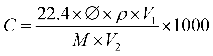
Electrical measurements of the as-fabricated sensors were carried out in a sealed chamber at RT (20 °C) which has been described in previous research.42 A 4200-SCS parameter analyser (Keithley) was utilised at the fixed voltage of 1 V as a biasing voltage to detect the resistance of the sensor. The overall experimental procedure, data acquisition, and control used in this research were similar to those used in previous work.41,42 The tested gases that were used in this study for characterising the selectivity characteristics together with NH3 for the as-fabricated sensor were in liquid form, where the concentration was diluted with deionized water. By using the static liquid gas distribution process, the essential concentration of the gas vapor was controlled and calculated by using the following equation:where C denotes the concentration of the target gas (ppm), ∅ denotes the volume fraction of the required gas, ρ denotes the liquid density (g ml−1), V1 denotes the liquid volume (μl), V2 denotes the chamber volume (l), and M denotes the molecular weight (g mol−1) of the liquids. The sensor response (S%) to the NH3 gas was calculated as AR = (R − Ra)/R, where Ra and R are the resistances of the sensor in response to synthetic air and NH3 gas at certain concentrations, respectively. The response–recovery time of the sensor was described as the time to reach 90% of its total resistance change. A testo 625 hygrometer (Testo, UK) was used to monitor the humidity level. A water bubble controller was used to vary the RH in the gas chamber.
Results and discussion
Thermal analysis and recovery of the precursor materials
The CuO nanoflakes were synthesised via a chemothermal route from the Cu foil recovered from waste FPCB as the precursor, using a TDT in the first step. The FPCB had the same polymer, PI [C35H28N2O7]n on both sides. To determine the optimum temperature for the TDT process, the thermal behaviour of the FPCBs was determined using TGA. In addition, the off-gas analysis was carried out using FTIR coupled with the TGA (Fig. S1(a) and (b), ESI†).In the TGA analysis of the FPCB, two distinctive degradation steps at 420 °C and 520 °C were observed. The PI in the FPCBs was attached to the Cu foil layer by layer with a resin/additive. In the literature, it was found that metallic Cu could have some thermocatalytic effect on the degradation of the polymer, which lowered the TDT temperature.2 In this thermocatalytic conversion, the PI degraded much faster at a lower temperature in the presence of metallic Cu, compared to degradation without copper.2,43 At 520 °C, a loss of ∼16.5% of the weight occurred due to the degradation, and after that the weight was constant. This means that the volatile materials in the FPCB were significantly lower compared to those in the conventional PCB, and the recovery process of Cu needs a significantly lower temperature when compared to smelting,1 making the process cost-effective. To characterise the volatile materials, the emitted gas was characterised by FTIR and GC-MS.
In an inert atmosphere and at a temperature range of 420 °C to 820 °C, the main decomposition products released by the PIs were about 50% non-volatiles and the remaining volatile compounds mainly consisted of CO2, CH4, CO, water, aromatic derivatives, and so on. About 28 wt% of PI was present in the FPCB waste, whereas under heat treatment in an inert atmosphere, ∼50–60% of the organic product was non-volatiles during the TDT process at 600 °C.
The FTIR analysis revealed that the decomposition of the PI from the waste FPCBs at 600 °C primarily released hydrocarbon and COx gases (Fig. S1(b), ESI†). From the FTIR spectra, it was shown that water was evolved over the whole range of temperatures, which indicated that, except for the adventitious moisture, this was a degradation product. The gas from the methyl groups started to release at ∼420 °C and the highest intensity was recorded at ∼520 °C. The gas released in the FTIR analysis can be explained from the two-step decomposition. At first, the end groups and the side groups of the PI degraded and generated CO, CO2, and CH4. Next, the main chain of the PI thermally transformed and released CO and CO2. The CO was generated directly from the imide ring while the release of CO2 could be explained in several ways, such as from imidisation or hydrolysis of amic acids, thermal decomposition of isoimide, undecomposed anhydrides, and so on.44 It is worth noting that the peaks from the benzonitrile group overlapped with the CO2 and CO peaks. When the pyrolysed product was collected by condensation during the TDT (600 °C) process it showed similar results. The benzonitrile was strongly detected in the product together with other aromatic hydrocarbons.
The condensed gas was analysed using a chromatogram obtained using GC-MS (Fig. S1(c), ESI†). The condensed gas had multiple compounds, as shown in the chromatogram (Fig. S1(c), ESI†). The peaks corresponding to the compounds are listed in Table 1. The main compositions were aromatic hydrocarbons and melamine, and the detected peaks corresponded to styrene, benzonitrile, indene, naphthalene, biphenyl, butylated hydroxytoluene, and acenaphthylene. High value carbon could be produced by this process, which could then be used in various industrial applications, such as energy storage.2
| Retention time (min) | Component | Retention time (min) | Component | ||
|---|---|---|---|---|---|
| 1 | 8.34 | Styrene (C8H8):organic compound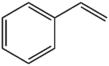 |
5 | 23.83 | Biphenyl (C12H10):aromatic hydrocarbon |
| 2 | 12.76 | Benzonitrile (C7H5N):melamine |
6 | 24.32 | Butylated hydroxytoluene (C15H24O) lipophilic organic compound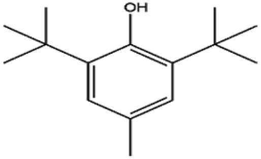 |
| 3 | 13.37 | Indene (C9H8):polycyclic aromatic hydrocarbon |
7 | 26.49 | Acenaphthylene (C12H8):polycyclic aromatic hydrocarbon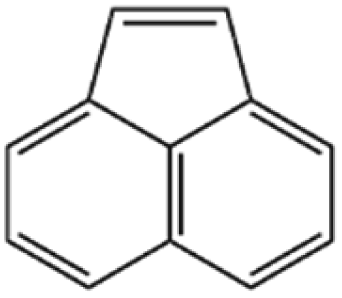 |
| 4 | 18.31 | Naphthalene (C10H8):polycyclic aromatic hydrocarbon |
Formation mechanism of the CuO nanoflakes
A schematic of the formation mechanism of the CuO nanoflakes by nucleation growth, orientation attachment,45 and the Ostwald ripening process46 are shown in Fig. 1.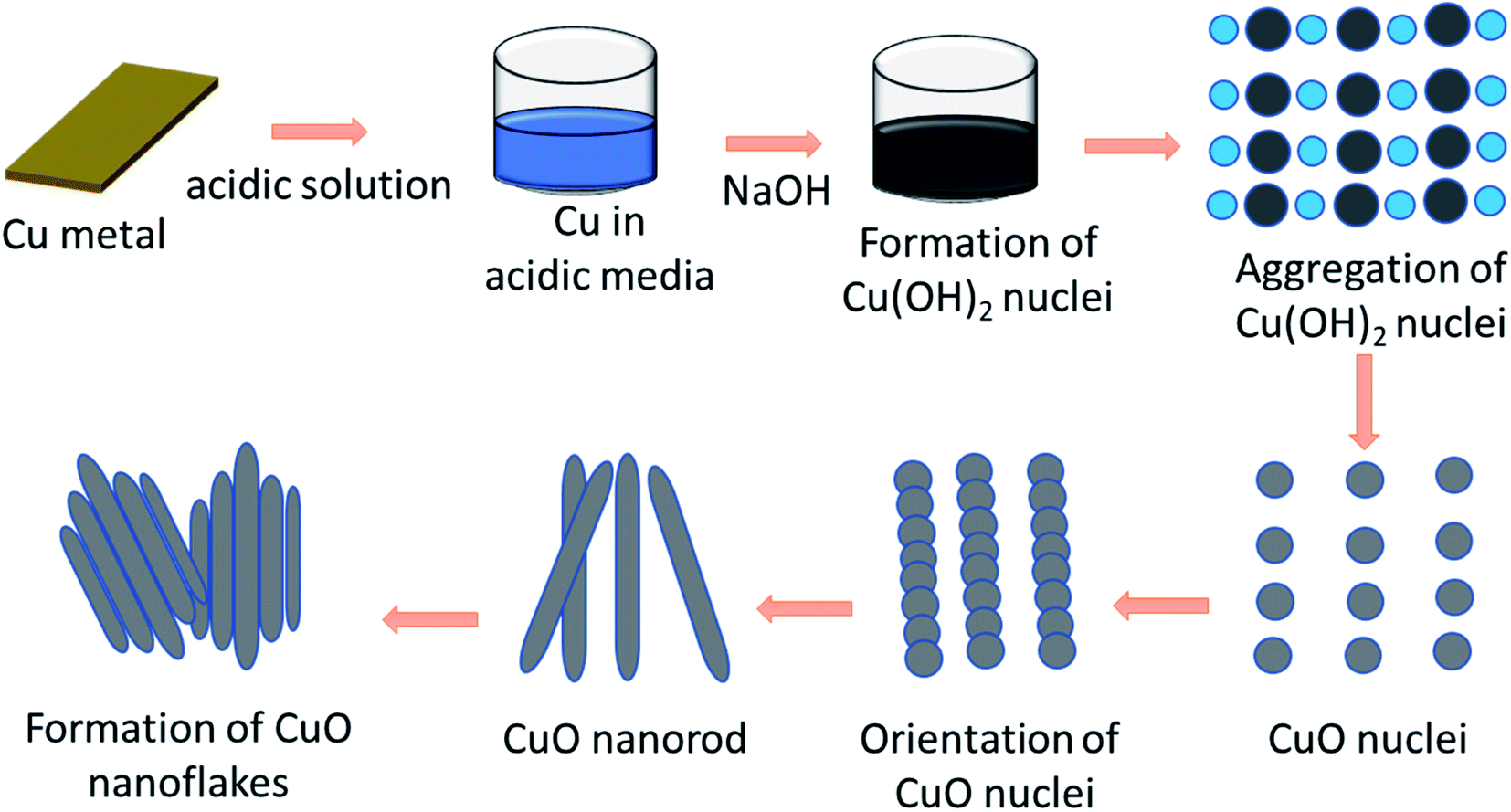 | ||
| Fig. 1 Schematic of the formation mechanism of the CuO nanoflakes. | ||
A plausible growth mechanism for this process includes the following major steps: the formation of the CuO nuclei happened by the dehydration of Cu(OH)2 nuclei upon heat treatment. The Ostwald ripening mechanism was involved wherein a thermodynamically driven process produced more stable, larger particles forms, from the smaller particles. After the formation of the CuO nuclei, the CuO molecules were attached by the mechanism of orientation aggregation and attachment. When the molecules were attached by this self-organisation in an ordered form, it shared a similar crystallographic pattern for reducing the energy which resulted in the formation of 1D nanorods. The nanorods were the building blocks of the nanoflakes. The CuO nanorods are assembled to form the aggregated bundles of nanorods which formed flake-like shapes.
Elemental analysis of the synthesised CuO nanoflakes
The recovered Cu was ∼96% pure with Ni ∼3% and some minor trace elements (Table 2). Often, a surface finish is essential for making a reliable connection between the FPCB and the electronic components by providing a solderable surface and protecting any exposed Cu from oxidising. Nickel emulsions were used for the surface finishing of the FCPBs, and this surface finish remained intact after the TDT process because the melting temperature of the emulsion was higher than the temperature used in the TDT process, meaning it was not separated from the FCPB with the carbonaceous residues. Therefore, the extracted Cu foil will have some remaining Ni emulsion during the synthesis of the CuO nanoflakes.| Element (wt%) | Cu | Ni | Zn | Sn | Mg | Si |
|---|---|---|---|---|---|---|
| ICP-OES | 96.4 | 3.54 | 0.02 | 0.02 | 0.01 | 0.01 |
| LIBS | 96.5 | 3.47 | 0.01 | 0.01 | 0.01 | <0.01 |
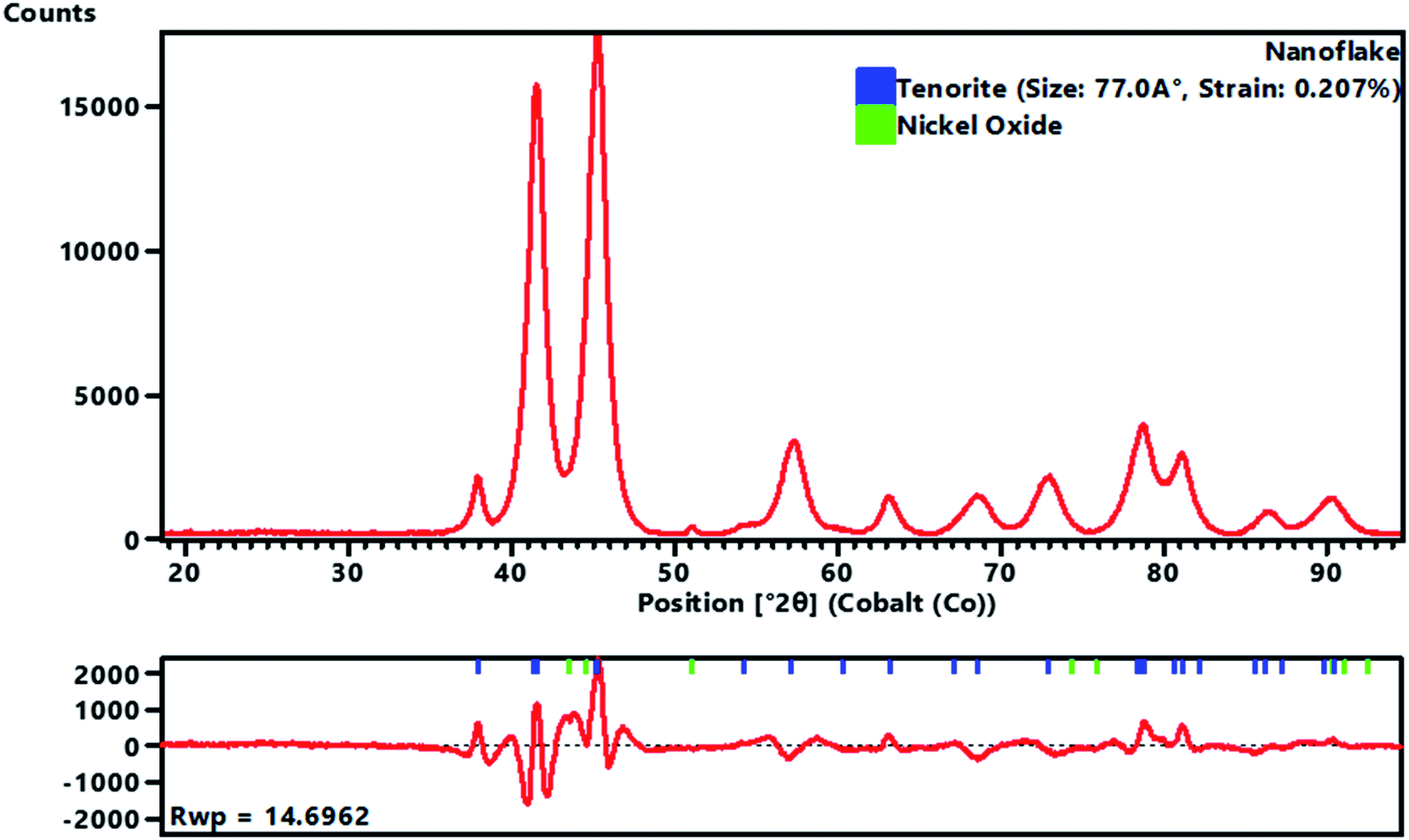
The XRD data for the nanoflakes was obtained using an Empyrean X-ray diffractometer (PANalytical) fitted with a Co tube and a PIXcel detector. The recorded powder XRD pattern was processed using HighScore Plus software (PANalytical BV) and then used for a candidate search match against the Inorganic Crystal Structure Database (ICSD), followed by a Rietveld fit to identify and quantitatively establish the abundances of tenorite (CuO) and NiO as shown in Fig. 2. An acceptable Rietveld fit was obtained with these two phases (Rwp: 9.91). The nanoflakes produced in the system were confirmed to be predominantly tenorite (CuO, 96.5% ± 2.5) with traces of NiO (3.5% ± 0.1).
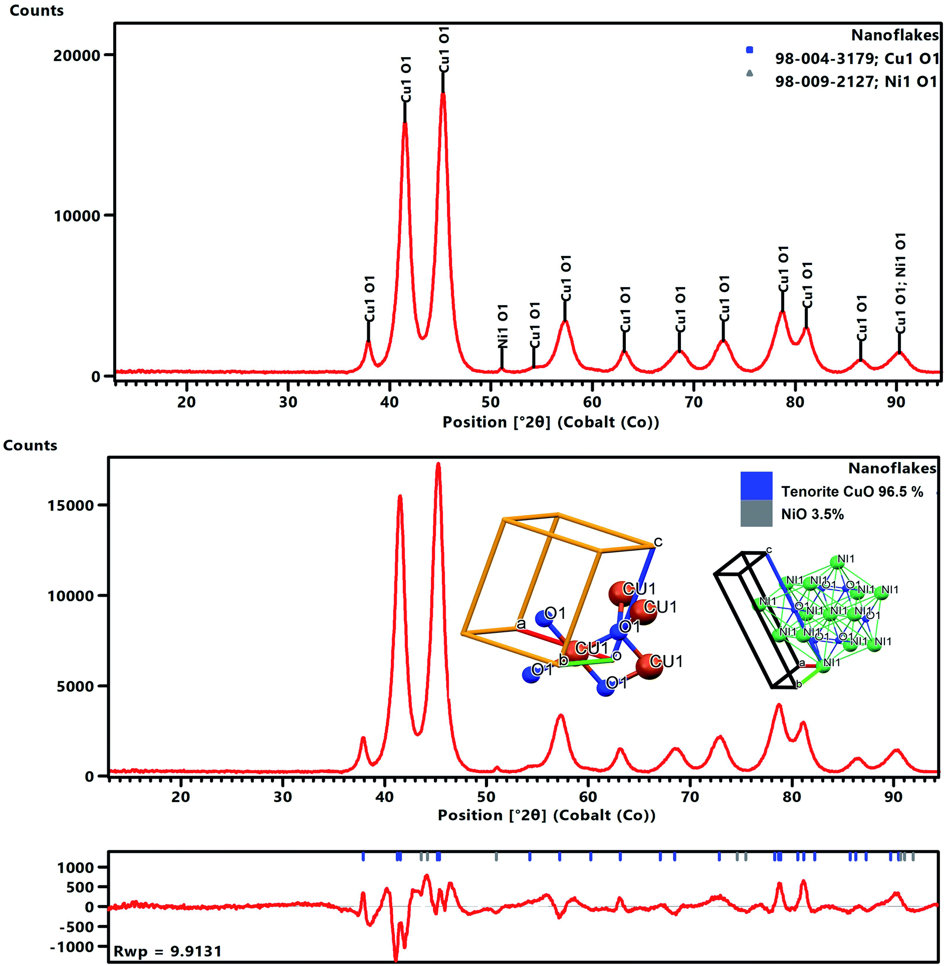 | ||
| Fig. 2 Processed XRD scans of the nanoflakes. Top: search match data with all the peaks explained by CuO as a major phase and NiO as a trace phase. Bottom: processed data after the Rietveld fit with relative abundances of tenorite (CuO) and NiO. Inset: The unit cell of Cu. | ||
After refinement, the lattice parameters were found to be: a = 4.696(2) Å, b = 3.414(3) Å, c = 5.137(9) Å, and β = 99.2°, with a cell volume of 81.31 (Å)3, and then these values were compared to ICSD data card values of a = 4.683(0) Å, b = 3.459(0) Å, c = 5.130(0) Å, and β = 99.309° with a cell volume of 81.29 (Å)3 for CuO.
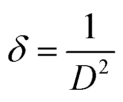
A full pattern Rietveld fit with size47 and strain-specific parameters48 was applied to estimate the average crystallite size and microstrain (Fig. 3). The instrument broadening was accounted for by measuring a Si 640c Silicon Standard. The CuO crystallite size was found to be 7.7 nm, and the associated microstrain was estimated as 0.207%. This suggested that the CuO crystallites were nanosized and had a dopant element of NiO in situ during the process. The dislocation density (δ) (defined as the length of the dislocation line per unit metre square) of the crystal was evaluated using eqn (4):
 | (4) |
 | ||
| Fig. 3 Full pattern Rietveld fit of the nanoflake scan for size and strain estimation. | ||
The obtained value of the dislocation density (length of dislocation lines per unit volume) of the crystal was δ = 0.0169, and the strain was εstr = 0.207%. This indicated a high level of crystallisation and high-quality CuO nanoflakes which may be suitable for use in photovoltaic applications. It was found that the strain arising from the lattice dislocation, and the dislocation density was very small, and had a negligible effect on the peak broadening of the CuO tetrapods. It is worth noting that the NiO phase was detectable in the XRD pattern, which proved that the precipitation of the NiO particles over the surface of the CuO nanoflakes had occurred. This phenomenon was often observed where the doping agents were high enough to precipitate and create a scaffold for fusion for further growth of the CuO crystallites. The surface morphology of the NiO doped CuO nanoflakes from the waste FPCBs is presented in Fig. S2, ESI.† The HR-SEM and EDS analysis results are also provided in Fig. S2 (ESI†). The EDS spectra clearly show the presence of the Cu, Ni, and O elements.
To reveal the chemical state of the FPCB-derived CuO nanoflakes, XPS analysis was carried out. The results of this analysis are shown in Fig. S5 (ESI†). The high-resolution XPS spectra clearly showed the existence of Cu2+ and Ni2+ components. The deconvolution of the high-resolution Cu2p3/2 showed five components at the binding energies of 933.5, 935.9, 941, 942.5, and 943.8. All these peaks correspond to the CuO chemical state. Three Ni2p3/2 peaks appeared at 855.49, ref. 49 861.17, ref. 50 and 864.07 ref. 50 which clearly corresponded to NiO. This analysis confirmed the presence of an in situ NiO dopant in the FPCB-derived CuO nanoflakes.51 The ICP and XRF analyses were also carried out, and the results indicated that the major elements of the nanoflakes were Cu with a 3–4% of Ni.
The microstructure, crystal structure, and elemental mapping of the NiO-doped CuO nanoflakes were investigated using HR-TEM imaging, selected are electron diffraction (SAED), and TEM-EDS analyses and the results are shown in Fig. 5(a)–(d). The nanoflakes demonstrated an irregular pattern and a feather-like morphology with a varied flake size. The irregular morphologies of the flakes were formed by assembling the many 1D nanorods which were visible in the HR-TEM images. As the flakes were not a single structure but the assembly of several 1D nanorods, the widths varied from ∼10 nm to 50 nm and the length varied from ∼30 nm to 80 nm. From the HR-TEM images, it is clearly seen that many rod-like particles are accumulated together to develop the structure of the nanoflakes, and could be ascribed to the well-known Ostwald ripening phenomena.46 In this procedure, at the beginning of the synthesis of the nanoflakes, particles ranging from small to large were generated in the non-equilibrium solution. The smaller particles dissolved easily and created free atoms which were transferred to the surface of the larger particles. This process continued because the larger crystals were energetically favourable compared to the smaller crystals, and promoted more solubility for the smaller crystals. The reprecipitation of the smaller crystal on the surface of the larger crystals created a compact structure that was favourable for the use of this CuO in solar cells for the transportation of a photocurrent. The CuO nanoflakes showed well-defined fringes, which were attributed to the single crystal of CuO. The measured lattice spacing was 2.75 Å, which was attributed to the (110) interplanar spacing. The SAED pattern also confirmed the absolute monoclinic structure, which corresponded to the XRD pattern. The TEM-EDS mapping showed the Cu and O distribution in the nanoflakes. To locate where the NiO particles were situated, STEM was performed. The bright-field image showed a single nanorod of which the nanoflakes are made. The NiO particles were not clearly visible in the bright-field image, however, the dark-field image clearly demonstrated the presence of NiO particles on the CuO nanoflakes which were uniformly distributed (Fig. S4, ESI†).
The porosity and the specific surface area of the CuO nanoflakes were measured using N2 isotherms for adsorption–desorption at 77.4 K and pore size distribution (BJH) measurements. The isotherm exhibited a type IV hysteresis, as shown in Fig. 4(e), and the relative pressure (P/Po) and loop were from 0.65 to 1.0, which further indicated that the structure was mesoporous. The CuO nanoflakes collected have a specific surface area of 115.703 m2 g−1, and the pore size distribution (BJH) indicated that the CuO nanoflakes have a mesoporous structure with an average pore diameter of 6 nm. The higher surface area has proven suitable for the gas sensing property.
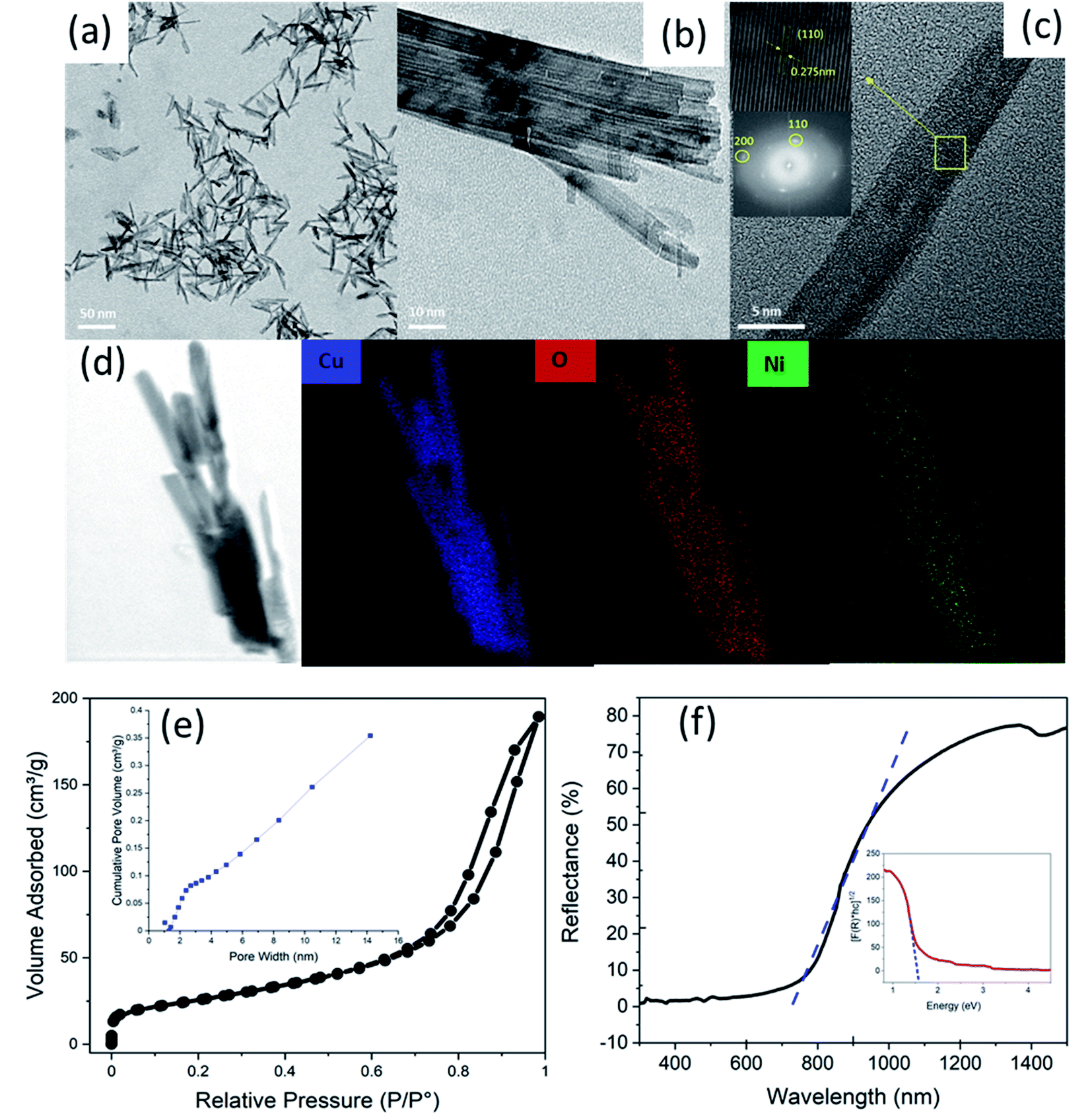 | ||
| Fig. 4 (a and b) The bright-field TEM image, (c) the lattice structure of the nano CuO flakes shown by the SAED pattern, (d) the TEM-EDS elemental mapping of the nanoflakes, (e) the isotherms for the N2 adsorption–desorption at 77.4 K and pore size distribution (inset), and (f) the UV-vis spectroscopy scan. | ||
The UV-vis spectroscopy is an important method for exploring the surface chemistry and assessing the suitability of nanomaterials for various applications. Fig. 4(f) shows a UV-vis diffuse reflectance spectrum of the CuO material synthesised in this research. The NiO doped CuO exhibited superior absorption in the region of the solar spectrum from 200 nm to 800 nm. In this region, the reflection was very low and near to a zero value. In the infrared region, with a wavelength greater than 800 nm, the reflectance was very high which was an indication of the superior gas sensitivity of the materials.52–54 The reflectivity of the sample depended on the absorption, reflectance, and scattering properties. The reflectivity of the CuO nanoparticles in the infrared region has been reported previously in the range of ∼20% to 80% depending upon the synthesis process with or without the dopant materials.52,55,56 In this study, the reflectivity was 75%.
A mathematical model was derived using the Kubelka–Munk theory to describe the reflectivity and the bandgap nature of an opaque sample. The relationship can be explained by the following equation:
 | (5) |
A Kubelka–Munk plot (also known as a Tauc plot) for the synthesised CuO is shown in Fig. 4(f). The linear part of the Tauc plot was used to estimate the indirect bandgap energy (Eg). The absorption edge for the NiO doped CuO in this research was at ∼690 nm in the visible range, whereas it was 344 nm for NiO in the UV range.57
The bandgap energy for CuO was 1.6 eV, which was higher than the value for bulk CuO (1.2 eV)57 and lower than that for the NiO nanoparticles (3.8 eV).51 The shift of the energy from one level to another could be attributed to quantum confinement in the nanocrystal structure. It has also been reported by several researchers that the combination of NiO and CuO can shift the bandgap to a higher region when compared to the pure CuO.36,38,39 Incorporating the NiO in the CuO nanoflakes in situ had given a wider bandgap that was suitable for the gas sensing property.58
The behaviour of sensors made from CuO nanomaterials for gas sensing, was because of the differences which occurred in the electric resistance due to the surface properties of adsorption/desorption of the gas.59 Certain parameters, such as the working temperature of the sensor, were also active in this mechanism. The surface adsorbed O2 molecules and formed O2−, O−, and O2− ions.60 This temperature-sensitive ion adsorption mechanism can be attributed to the surface acceptor condition that occurred because of the O2 adsorption. The adsorption of O2 entrapped the e− from the valence band and in return, enhanced the accumulation of holes, which further boosted the concentration of the electrical carriers. When the CuO nanoflake surface was exposed to a reducing gas, such as NH3, the oxygen ions and the NH3 interacted with each other and induced the electron to return back to the valence band. This phenomenon reduced the number of holes, and increased the resistance.
The NH3 gas sensing mechanism using a NiO doped CuO nanoflake based sensor
Previous research reported in the literature revealed that the sensing mechanism for metal oxides with/without targeted gas could be attributed to the modulation of electric conductivity, which was basically composed of three processes such as adsorption/desorption and a charge transfer mechanism. The theory of electron depletion region revealed that the electrons were trapped within the surface of NiO from the conduction band in the air medium, by adsorbing the oxygen molecules and forming numerous ionised systems including O2−, O−, O2− and causing the reduction in the electrical conductivity of the gas sensor (adsorption kinetics in eqn (6), (7) and (8)).| O2 + Sads ↔ O2ads | (6) |
| O2ads + 2e− ↔ 2Oads− | (7) |
| O2ads + e− ↔ O2− | (8) |
To enhance the sensing characteristics by adsorbing more oxygen molecules on to the surface of the metal oxide structures, it is important to enhance the active sites on the surface of the metal oxide structures by increasing the porosity within the sensing materials. In this study, microrecycled NiO doped CuO has a high porosity (refer to the BET results) which helps to enhance the number of active sites, which leads to a superior response of the NH3 gas molecules (eqn (9) and (10)):61
| 2NH3 + 6h+ + 3O− → N2 + 3H2O | (9) |
| 2NH3 + 3O− → N2 + 3H2O + 3e− | (10) |
The advancement of the sensing characteristics in terms of sensor response for the NiO doped CuO-based NH3 sensor is attributed to the depletion layer, which was formed at the p–n junction at the interface of NiO and CuO. Importantly, the electron flow was controlled by the depletion layers between the NiO and CuO by adsorbing the ionized oxygen at the surface of the NiO (Fig. 5). In the NH3 gas medium, the NiO–CuO sensor captured and transferred electrons into the sensing materials and consumed the holes in CuO. As a result, the excess electrons lead to NiO and decreased the thickness of the depletion layer. Because of the presence of the p–h junction in between the metal oxides, the absorbed holes in CuO supplemented from the depletion layer to p–n junction. During this phenomenon, the consumed electrons travelled into the conduction band and the holes in the NiO/CuO hetero-junction drift to the CuO crosswise hetero-contact interface that increased the concentration of charge carriers and resulted in a contraction in resistivity.62
 | ||
| Fig. 5 A schematic of the NH3 gas-sensing process of the NiO doped CuO nanoflake sensor. | ||
The NH3 gas sensing characteristics of the NiO doped CuO nanoflake based sensor
The NiO doped CuO performs an important function in NH3 gas sensing due to the formation of the depletion region. Contemplating the noteworthy benefit of the porous nano/microstructure in heterojunction-based gas sensors, highly porous NiO doped CuO films were fabricated to investigate several volatile organic compounds (VOCs), and NH3 at RT. Fig. 6(a) illustrates the dynamic gas sensing response of NiO–CuO-based sensors using NH3 gas at a parts per million (ppm) concentration at RT. The NiO–CuO sensor responded well to the increased NH3 concentration. The NiO–CuO-based sensor showed an excellent response which was linearly correlated with the concentration at a low range of NH3 (25–500 ppm). The sensor did not experience any mechanical deformation at a very low level of NH3 (25 ppm) which was attributed to the clamping effect, justified by the tensile stiffness of a laminated specimen .63 As a result, at the lowest concentration of NH3 gas, swelling of the NiO doped CuO occurs, which gave a modest signal-to-noise ratio (SNR) with insignificant hysteretic behaviour. As stated, previously, the relationship between the sensor response and the gas concentration at ppm levels at RT showed a linear trend and this is shown in Fig. 6(b). Fig. 6(c) shows the repeatability and reproducibility behaviour of the as-fabricated sensors. One more significant factor of the NH3 sensor is the response–recovery time characteristics. The fast response of the sensor, as well as its swift recovery, is required for real-time applications. Fig. 6(d) shows the response–recovery time characteristics of the NiO–CuO-based NH3 sensor. For 200 ppm of NH3 gas, the calculated response and recovery times were 11.7 s and 21.5 s, respectively.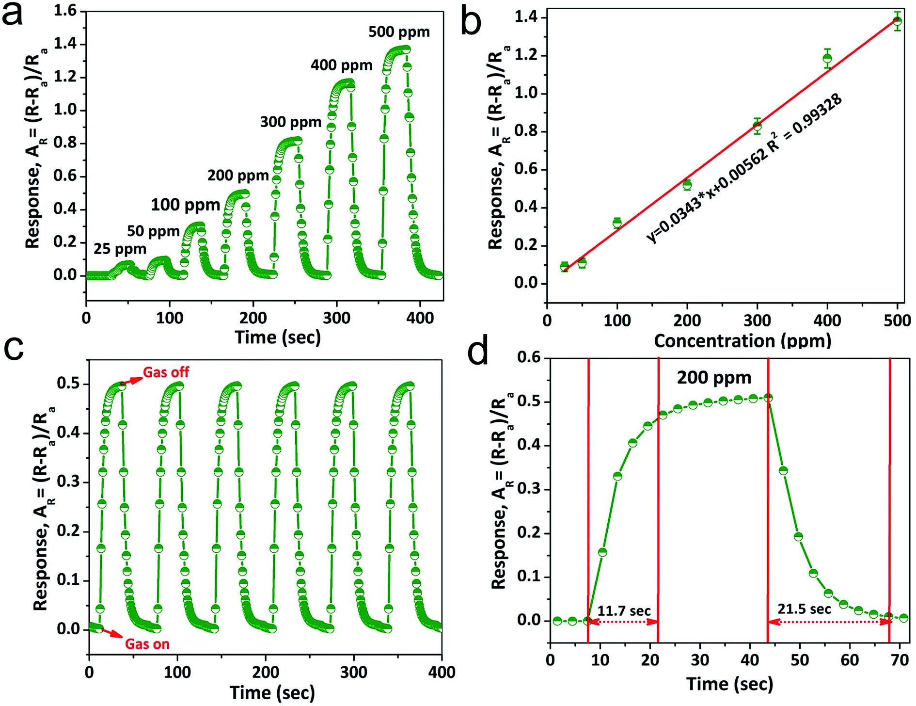 | ||
| Fig. 6 (a) Dynamic response, and (b) the linear correlation characteristics of the NiO doped CuO sensor to various concentrations of NH3 gas at RT (20 °C). (c) Repeatability, and (d) response–recovery time characteristics of NiO doped CuO sensor to 200 ppm of NH3 gas. | ||
The sensor response characteristics of the NiO doped CuO-based sensor for several VOC biomarkers were investigated at RT and the results are shown in Fig. 7(a). The investigation revealed that the NiO doped CuO-based sensor exhibited a superior response to NH3 gas at RT. The responses (AR) of 0.511, 0.033, 0.032.87, 0.018, 0.011, 0.098, 0.0904, 0.0897 and 0.07 were calculated for ammonia, acetone, ethanol, methanol, isopropanol, n-butanol, acetyl-acetone, gasoline, and xylene respectively. The response to the NH3 gas is supposed to occur because of the adsorption of the moisture through the activation of the CuO film. The overall effect is to reduce the resistance of the film, and this difference in resistance gives a response to NH3 gas at RT. At RT, the oxygen adsorption will not take place. Hence, the sensing mechanism would not be carried out by the oxygen adsorption/desorption. As the temperature increases above the RT, the moisture of the surface will be reduced by evaporation which further reduced the sensor response. At this stage, an exothermic reaction could take place spontaneously between NiO doped CuO and NH3 at a certain temperature, offering adequate surface energy to overcome the bond energy of NH3. Furthermore, the increase in the bond energies compared to NH3 caused less sensitivity to other VOC biomarkers. However, the reactions between the NiO doped CuO and other test gases were endothermic and could not be spontaneous, resulting in reduced sensor responses.
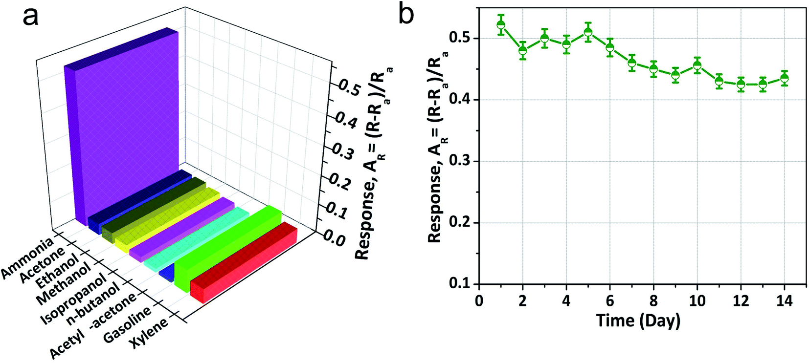 | ||
| Fig. 7 (a) The NiO doped CuO sensor showing the response for various VOC biomarkers at gas concentrations of 200 ppm at RT (20 °C). (b) Long-term stability of the NiO doped CuO sensor to 200 ppm of NH3 gas at RT (20 °C). | ||
The long term stability of the sensor is important to be able to define its application in the real world. In this study, to determine the stability, the fabricated sensor was tested for two weeks (14 d) by exposing it to 500 ppm of NH3 gas at RT and it was found that the response value of this sensor did not degrade notably throughout the whole period (Fig. 7(b)), which suggested that the as-fabricated sensor had superior stability.
Humidity is one of the vital parameters for the gas sensing characteristics for real-world sensor applications. In this study, the humidity effect on the NiO doped CuO senor was investigated at RT (20 °C). It is worth noting that for NH3 sensing both NH3 and water molecules act as oxidising agents, which increased the resultant sensor response. During the characterizations, the RH of the open-air environment was about 15% at RT. The effect of RH to the sensor response of the as-fabricated sensor to 200 ppm of NH3 gas is shown in Fig. 8. It was observed from Fig. 8, that the resultant response of the as-fabricated sensor increased with the concentration of water molecules. The as-fabricated NH3 gas sensors were compared to other available sensors which demonstrated enhanced responses, superior sensitivity together with fast response time characteristics. A comparison is shown in Table 3.
 | ||
| Fig. 8 Effect of relative humidity on the response of the NiO doped CuO sensor to 200 ppm of NH3 gas at RT (20 °C). | ||
| Sensing material | Ammonia gas concentration (ppm) | Operating temp. (°C) | Sensor response (%) | Ref. |
|---|---|---|---|---|
| Cellulose/TiO2/PANI composite nanofibers | 100 | RT | 3.5 | 64 |
| CeO2 NP@PANI | 100 | RT | 11 | 65 |
| PA6/TiO2/PANI | 100 | RT | 1 | 66 |
| n-MoS2/p-CuO heterojunction nanoworms | 100 | RT | 17 | 67 |
| PbS quantum dots/TiO2 nanotube arrays | 100 | RT | 17.4 | 68 |
| CuO activated ZnO films | 100 | RT | 12 | 6 |
| PVP/CuO nanocomposite | 200 | RT | 17 | 69 |
| 3D printed CuO | 200 | RT | 14.17 | 70 |
| Carbon nanotubes | 100 | RT | 6 | 8 |
| NiO doped CuO nanoflakes | 200 | RT | 31.74 | This work |
Conclusions
In summary, NiO doped CuO 2D nanoflakes made via the assembly of 1D nanorods with a high surface area of 115.703 m2 g−1 were selectively synthesised from waste flexible printed circuit boards for use in applications requiring gas sensors. By using this microrecycled material, gas sensors were successfully developed and their sensing performance to NH3 was characterized, which showed good sensing characteristics including fast response (11.7 s) and recovery (21.5 s) time, high response values, and superior selectivity to 200 ppm of NH3 gas at room temperature (20 °C). The as-fabricated sensors had a wide range of detection from 25 ppm to 500 ppm with good repeatability and durability. Finally, this study showed the great potential of the NiO doped CuO 2D nanoflakes made by the assembly of 1D nanorods, in the fabrication of inexpensive and low-power sensors for use as a significant sensing material for fast and selective detection of NH3, which overcomes the long-standing challenges of real-world sensor applications.Author contributions
Rumana Hossain: conceptualisation, experiments, formal analysis, writing: original draft, review and editing. Kamrul Hassan: conceptualisation, experiments, formal analysis, writing: original draft, review and editing. Veena Sahajwalla: conceptualisation, formal analysis, writing: review and editing, supervision, project administration, funding acquisition.Funding
This research was supported by the Australian Research Council's Industrial Transformation Research Hub funding scheme (Project No. IH190100009).Availability of data and materials
Data and research materials are available on request.Conflicts of interest
The authors declare no conflicts of interest.Acknowledgements
The technical support for this research was provided by the UNSW Mark Wainwright Analytical Centre (Australia).References
- V. Sahajwalla and R. Hossain, The science of microrecycling: a review of selective synthesis of materials from electronic waste, Mater. Today Sustain., 2020, 9, 100040 CrossRef.
- R. Hossain and V. Sahajwalla, Microrecycling of waste flexible printed circuit boards for in-situ generation of O-and N-doped activated carbon with outstanding supercapacitance performance, Resour., Conserv. Recycl., 2021, 167, 105221 CrossRef CAS.
- R. Hossain, et al., Sustainable recovery of Cu and Sn from problematic global waste: exploring value from waste printed circuit boards, ACS Sustainable Chem. Eng., 2018, 7(1), 1006–1017 CrossRef.
- J. W. Kim, et al., En masse pyrolysis of flexible printed circuit board wastes quantitatively yielding environmental resources, J. Hazard. Mater., 2018, 342, 51–57 CrossRef CAS PubMed.
- A. Al Mahmood, R. Hossain and V. Sahajwalla, Investigation of the effect of laminated polymers in the metallic packaging materials on the recycling of aluminum by thermal disengagement technology (TDT), J. Cleaner Prod., 2020, 274, 122541 CrossRef CAS.
- A. Al Mahmood, R. Hossain and V. Sahajwalla, Microrecycling of the metal–polymer-laminated packaging materials via thermal disengagement technology, SN Appl. Sci., 2019, 1(9), 1–19 Search PubMed.
- S. Yousef, et al., A strategy for synthesis of copper nanoparticles from recovered metal of waste printed circuit boards, J. Cleaner Prod., 2018, 185, 653–664 CrossRef CAS.
- N. V. Mdlovu, et al., Recycling copper nanoparticles from printed circuit board waste etchants via a microemulsion process, J. Cleaner Prod., 2018, 185, 781–796 CrossRef CAS.
- F.-R. Xiu, et al., A novel recovery method of copper from waste printed circuit boards by supercritical methanol process: Preparation of ultrafine copper materials, Waste Manage., 2017, 60, 643–651 CrossRef CAS PubMed.
- R. S. El-Nasr, et al., Environmentally friendly synthesis of copper nanoparticles from waste printed circuit boards, Sep. Purif. Technol., 2020, 230, 115860 CrossRef.
- O. Fouad and S. A. Basir, Cementation-induced recovery of self-assembled ultrafine copper powders from spent etching solutions of printed circuit boards, Powder Technol., 2005, 159(3), 127–134 CrossRef CAS.
- F.-R. Xiu and F.-S. Zhang, Preparation of nano-Cu2O/TiO2 photocatalyst from waste printed circuit boards by electrokinetic process, J. Hazard. Mater., 2009, 172(2–3), 1458–1463 CrossRef CAS PubMed.
- X. Zhang, et al., Different CuO nanostructures: synthesis, characterization, and applications for glucose sensors, J. Phys. Chem. C, 2008, 112(43), 16845–16849 CrossRef CAS.
- S. Anandan and S. Yang, Emergent methods to synthesize and characterize semiconductor CuO nanoparticles with various morphologies–an overview, J. Exp. Nanosci., 2007, 2(1–2), 23–56 CrossRef CAS.
- A. Li, et al., Enhanced lithium storage performance of hierarchical CuO nanomaterials with surface fractal characteristics, Appl. Surf. Sci., 2018, 443, 382–388 CrossRef CAS.
- C.-T. Hsieh, et al., Field emission from various CuO nanostructures, Appl. Phys. Lett., 2003, 83(16), 3383–3385 CrossRef CAS.
- G. Qiu, et al., Facile microwave-assisted hydrothermal synthesis of CuO nanomaterials and their catalytic and electrochemical properties, J. Phys. Chem. C, 2012, 116(1), 468–477 CrossRef CAS.
- M. P. Choudhary and V. Garg. Causes, consequences and control of air pollution. in All India seminar on methodologies for air pollution control, Jaipur, Rajasthan, 2013 Search PubMed.
- B. Inanloo and B. Tansel, Explosion impacts during transport of hazardous cargo: GIS-based characterization of overpressure impacts and delineation of flammable zones for ammonia, J. Environ. Manage., 2015, 156, 1–9 CrossRef PubMed.
- E. Kirk, Amino acid and ammonia metabolism in liver diseases, Acta Med. Scand., 1936, 89, 77–147 Search PubMed.
- N. M. Abu-Elala, et al., Eutrophication, ammonia intoxication, and infectious diseases: interdisciplinary factors of mass mortalities in cultured Nile tilapia, J. Aquat. Anim. Health, 2016, 28(3), 187–198 CrossRef CAS PubMed.
- J. E. Ryer-Powder, Health effects of ammonia, Plant/Oper. Prog., 1991, 10(4), 228–232 CrossRef CAS.
- M.-Z. Dai, et al., Highly sensitive ammonia sensor with organic vertical nanojunctions for noninvasive detection of hepatic injury, Anal. Chem., 2013, 85(6), 3110–3117 CrossRef CAS PubMed.
- Z. Jin, Y. Su and Y. Duan, Development of a polyaniline-based optical ammonia sensor, Sens. Actuators, B, 2001, 72(1), 75–79 CrossRef CAS.
- D. Lv, et al., Enhanced flexible room temperature ammonia sensor based on PEDOT: PSS thin film with FeCl3 additives prepared by inkjet printing, Sens. Actuators, B, 2019, 298, 126890 CrossRef CAS.
- E. Connolly, et al., A porous SiC ammonia sensor, Sens. Actuators, B, 2005, 109(1), 44–46 CrossRef CAS.
- M. Aslam, et al., A highly selective ammonia gas sensor using surface-ruthenated zinc oxide, Sens. Actuators, A, 1999, 75(2), 162–167 CrossRef CAS.
- V. Chabukswar, S. Pethkar and A. A. Athawale, Acrylic acid doped polyaniline as an ammonia sensor, Sens. Actuators, B, 2001, 77(3), 657–663 CrossRef CAS.
- Y. Li, F. Yang and Y. Yu, LSDA+ U study on the electronic and anti-ferromagnetic properties of Ni-doped CuO and Cu-doped NiO, Chin. J. Catal., 2017, 38(5), 767–773 CrossRef CAS.
- A. Turky, Electrical surface and catalytic properties of NiO as influenced by doping with CuO and Ag2O, Appl. Catal., A, 2003, 247(1), 83–93 CrossRef CAS.
- L. M. Dwivedi, et al., Gum Acacia modified Ni doped CuO nanoparticles: an excellent antibacterial material, J. Cluster Sci., 2021, 32(1), 209–219 CrossRef CAS.
- M. Chandrasekar, et al., Synthesis and characterization studies of pure and Ni doped CuO nanoparticles by hydrothermal method, J. King Saud Univ. Sci., 2022, 101831 CrossRef.
- C. Thangamani, et al., Magnetic behavior of ni-doped cuo nanoparticles synthesized by microwave irradiation method, Surf. Rev. Lett., 2019, 26(05), 1850184 CrossRef CAS.
- Q. Zhang, et al., CuO nanostructures: synthesis, characterization, growth mechanisms, fundamental properties, and applications, Prog. Mater. Sci., 2014, 60, 208–337 CrossRef CAS.
- P. Raksa, et al., Ethanol sensing properties of CuO nanowires prepared by an oxidation reaction, Ceram. Int., 2009, 35(2), 649–652 CrossRef CAS.
- T. Adinaveen, T. Karnan and S. A. S. Selvakumar, Photocatalytic and optical properties of NiO added Nephelium lappaceum L. peel extract: An attempt to convert waste to a valuable product, Heliyon, 2019, 5(5), e01751 CrossRef CAS PubMed.
- M. Shi, et al., Temperature-controlled crystal size of wide band gap nickel oxide and its application in electrochromism, Micromachines, 2021, 12(1), 80 CrossRef PubMed.
- S. M. Meybodi, et al., Synthesis of wide band gap nanocrystalline NiO powder via a sonochemical method, Ultrason. Sonochem., 2012, 19(4), 841–845 CrossRef PubMed.
- S. Senobari and A. Nezamzadeh-Ejhieh, A comprehensive study on the enhanced photocatalytic activity of CuO-NiO nanoparticles: designing the experiments, J. Mol. Liq., 2018, 261, 208–217 CrossRef CAS.
- K. Hassan, et al., Microrecycled zinc oxide nanoparticles (ZnO NP) recovered from spent Zn–C batteries for VOC detection using ZnO sensor, Anal. Chim. Acta, 2021, 1165, 338563 CrossRef CAS PubMed.
- K. Hassan, R. Hossain and V. Sahajwalla, Novel microrecycled ZnO nanoparticles decorated macroporous 3D graphene hybrid aerogel for efficient detection of NO2 at room temperature, Sens. Actuators, B, 2021, 330, 129278 CrossRef CAS.
- K. Hassan and G.-S. Chung, Catalytically activated quantum-size Pt/Pd bimetallic core–shell nanoparticles decorated on ZnO nanorod clusters for accelerated hydrogen gas detection, Sens. Actuators, B, 2017, 239, 824–833 CrossRef CAS.
- R. Hossain, A. Al Mahmood and V. Sahajwalla, Facile Solution for Recycling Hazardous Flexible Plastic-Laminated Metal Packaging Waste To Produce Value-Added Metal Alloys, ACS Sustainable Chem. Eng., 2021, 9(50), 16881–16895 CrossRef CAS.
- W. Xie and W.-P. Pan, Thermal characterization of materials using evolved gas analysis, J. Therm. Anal. Calorim., 2001, 65(3), 669–685 CrossRef CAS.
- A. V. Salkar, et al., NH-and CH-Substituted Ureas as Self-Assembly Directing Motifs for Facile Synthesis and Electrocapacitive Applications of Advanced WO3–x One-Dimensional Nanorods, ACS Appl. Energy Mater., 2019, 2(12), 8724–8736 CrossRef CAS.
- A. Kabalnov, Ostwald ripening and related phenomena, J. Dispersion Sci. Technol., 2001, 22(1), 1–12 CrossRef CAS.
- L. Lutterotti and P. Scardi, Simultaneous structure and size–strain refinement by the Rietveld method, J. Appl. Crystallogr., 1990, 23(4), 246–252 CrossRef CAS.
- I. Fahim, et al., Chemical preparation and XRD data for a new triphosphate CuNa3P3O10 and two cyclotriphosphates SrRbP3O9 3H2O and SrRbP3O9, Powder Diffr., 2011, 26(1), 78–81 CrossRef CAS.
- G. Ertl, et al., XPS study of copper aluminate catalysts, Appl. Surf. Sci., 1980, 5(1), 49–64 CrossRef CAS.
- A. Mansour, Characterization of NiO by XPS, Surf. Sci. Spectra, 1994, 3(3), 231–238 CrossRef CAS.
- Q. Hu, et al., Hollow Cu-doped NiO microspheres as anode materials with enhanced lithium storage performance, RSC Adv., 2019, 9(36), 20963–20967 RSC.
- R. Shabu, et al., Assessment of CuO thin films for its suitability as window absorbing layer in solar cell fabrications, Mater. Res. Bull., 2015, 68, 1–8 CrossRef CAS.
- Z. A. Zaky, et al., Refractive index gas sensor based on the Tamm state in a one-dimensional photonic crystal: theoretical optimisation, Sci. Rep., 2020, 10(1), 1–9 CrossRef PubMed.
- C. Yang, et al., Gas sensing properties of CuO nanorods synthesized by a microwave-assisted hydrothermal method, Sens. Actuators, B, 2011, 158(1), 299–303 CrossRef CAS.
- M. R. Parra and F. Z. Haque, Structural and optical properties of poly-vinylpyrrolidone modified ZnO nanorods synthesized through simple hydrothermal process, Optik, 2014, 125(17), 4629–4632 CrossRef.
- Y.-B. Zhang, et al., Enhanced ethanol gas-sensing properties of flower-like p-CuO/n-ZnO heterojunction nanorods, Sens. Actuators, B, 2014, 202, 500–507 CrossRef CAS.
- K. Varunkumar, et al., Effect of calcination temperature on Cu doped NiO nanoparticles prepared via wet-chemical method: structural, optical and morphological studies, Mater. Sci. Semicond. Process., 2017, 66, 149–156 CrossRef CAS.
- A. Umar, et al., CuO nanosheets as potential scaffolds for gas sensing applications, Sens. Actuators, B, 2017, 250, 24–31 CrossRef CAS.
- N. Barsan, et al., Modeling of sensing and transduction for p-type semiconducting metal oxide based gas sensors, J. Electroceram., 2010, 25(1), 11–19 CrossRef CAS.
- T. T. Trinh, et al., Improving the ethanol sensing of ZnO nano-particle thin films—the correlation between the grain size and the sensing mechanism, Sens. Actuators, B, 2011, 152(1), 73–81 CrossRef CAS.
- M. Poloju, N. Jayababu and M. R. Reddy, Improved gas sensing performance of Al doped ZnO/CuO nanocomposite based ammonia gas sensor, Mater. Sci. Eng. B, 2018, 227, 61–67 CrossRef CAS.
- C. Wang, et al., Reduced graphene oxide decorated with CuO–ZnO hetero-junctions: towards high selective gas-sensing property to acetone, J. Mater. Chem. A, 2014, 2(43), 18635–18643 RSC.
- K. Lundström, M. Shivaraman and C. Svensson, A hydrogen-sensitive Pd-gate MOS transistor, J. Appl. Phys., 1975, 46(9), 3876–3881 CrossRef.
- Z. Pang, et al., A room temperature ammonia gas sensor based on cellulose/TiO2/PANI composite nanofibers, Colloids Surf., A, 2016, 494, 248–255 CrossRef CAS.
- L. Wang, et al., Enhanced sensitivity and stability of room-temperature NH3 sensors using core–shell CeO2 nanoparticles@ cross-linked PANI with p–n heterojunctions, ACS Appl. Mater. Interfaces, 2014, 6(16), 14131–14140 CrossRef CAS PubMed.
- Z. Pang, et al., Fabrication of PA6/TiO2/PANI composite nanofibers by electrospinning–electrospraying for ammonia sensor, Colloids Surf., A, 2014, 461, 113–118 CrossRef CAS.
- S. Sharma, et al., Excellent room temperature ammonia gas sensing properties of n-MoS2/p-CuO heterojunction nanoworms, Sens. Actuators, B, 2018, 275, 499–507 CrossRef CAS.
- Y. Liu, et al., Highly sensitive and selective ammonia gas sensors based on PbS quantum dots/TiO2 nanotube arrays at room temperature, Sens. Actuators, B, 2016, 236, 529–536 CrossRef CAS.
- H. U. Khan, et al., Inquest of highly sensitive, selective and stable ammonia (NH3) gas sensor: Structural, morphological and gas sensing properties of polyvinylpyrrolidone (PVP)/CuO nanocomposite, Synth. Met., 2020, 268, 116482 CrossRef.
- G. Chaloeipote, et al., 3D printed CuO semiconducting gas sensor for ammonia detection at room temperature, Mater. Sci. Semicond. Process., 2021, 123, 105546 CrossRef CAS.
Footnotes |
| † Electronic supplementary information (ESI) available. See https://doi.org/10.1039/d1na00743b |
| ‡ Authors have equal contributions. |
| This journal is © The Royal Society of Chemistry 2022 |