
 Open Access Article
 This Open Access Article is licensed under a Creative Commons Attribution-Non Commercial 3.0 Unported Licence
An efficient organic and inorganic hybrid interlayer for high performance inverted red cadmium-free quantum dot light-emitting diodes†
Nagarjuna Naik
Mude
,
Su Jeong
Kim
,
Raju
Lampande
and
Jang Hyuk
Kwon
 *
*
Department of Information Display, Kyung Hee University, 26, Kyungheedae-ro, Dongdaemoon-gu, Seoul, 130-701, Republic of Korea. E-mail: jhkwon@khu.ac.kr
First published on 18th December 2021
Abstract
The efficiency and device lifetime of quantum dot light-emitting diode (QLED) devices suffer from the charge imbalance issue resulting from excess electron injection from the ZnO electron transport layer (ETL) to the quantum dot (QD) emissive layer (EML). Herein we report 1,3-bis(9-phenyl-1,10-phenanthrolin-2-yl)benzene (BPPB) small molecule ETL blended ZnO as an interlayer in inverted red indium phosphide (InP) based QLEDs to slow down the ZnO ETL mobility. The device with ZnO![[thin space (1/6-em)]](https://www.rsc.org/images/entities/char_2009.gif) :BPPB (15 wt%) shows 16.7% external quantum efficiency and 595 h lifetime (T50) at 1000 cd m−2. Insertion of a thin hybrid interlayer reduces the electron injection to match the charge balance in the QD layer and also suppresses the interfacial exciton quenching between the ZnO ETL and QD EML.
:BPPB (15 wt%) shows 16.7% external quantum efficiency and 595 h lifetime (T50) at 1000 cd m−2. Insertion of a thin hybrid interlayer reduces the electron injection to match the charge balance in the QD layer and also suppresses the interfacial exciton quenching between the ZnO ETL and QD EML.
Introduction
Quantum dot light-emitting diodes (QLEDs) have rapidly gained tremendous attention in the development of solid-state lighting and future display applications due to their many beneficial properties such as high transparency, high color purity, high stability, and flexibility.1–6 Many researchers have been focusing on improving cadmium-free QLED device performance. One of the reasons for such poor performances is that the electron and hole injection imbalance in the quantum dot (QD) emissive layer (EML) causes quenching.7–13 Therefore, charge balance plays a key role in improving the performance of the device.Because of the low barrier to electron injection and high electron mobility, ZnO led to excess electron injection resulting in a severe charge imbalance issue in the QD EML.14–16 As well as charge imbalance, there is also exciton quenching of the QD EML, which is induced by the adjacent ZnO layer due to spontaneous charge transfer.24,32,33 To solve such issues, it is necessary modulate electron injection to attain proper charge balance within the QD EML and also reduce spontaneous charge transfer to suppress exciton quenching of the QD. Following this approach, Peng. et al. inserted an ultra-thin insulating poly (methyl methacrylate) (PMMA) layer with a thickness of 6 nm between the ZnO electron transport layer (ETL) and QD EML.17 Wang. et al. utilized a polyethyleneimine (PEI) insulator to reduce the electron injection and quenching by charge transfer at ZnO in inverted QLED devices.18 Although excellent device performances with such insulating layers had been achieved, such an approach is too much sensitive to the thickness of the insulating layer. Another simple and effective approach is to modulate the electronic structures of ZnO by doping metals such as magnesium (Mg), yttrium (Y), gallium (Ga), and aluminium (Al) to improve the charge balance or suppress the exciton quenching of the QD interface.19–23 Cesium azide (CsN3),24 polyvinylpyrrolidone (PVP),25 and lithium 8-quinolate (LiQ)26 materials also have been studied as dopants to modulate the mobility of ZnO. To improve the device performance of the device with insulating or organic polymer interlayers, thickness control is crucial, which forms a tunneling barrier in the QLED device.7
We report a high efficiency inverted red device using an organic and inorganic hybrid interlayer. This hybrid interlayer reduces the electron injection and enhances the charge balance. Most organic ETLs used in organic light-emitting devices (OLEDs) have lower electron mobility, around ∼10−4 cm2 V−1 s−1, and also have the shallower lowest unoccupied molecular orbital (LUMO) energy level.27 Hence, mixing the organic ETL and ZnO could provide slow electron mobility because of the nature of the organic ETL and delayed electron transport because of the shallow LUMO level. In addition, it could reduce interface quenching by charge transfer in the devices. Among several small molecule (SM) ETL materials, we investigated a good miscible material in terms of solubility, film morphology, dissolution etc. As the best material, 1,3-bis(9-phenyl-1,10-phenanthrolin-2-yl)benzene (BPPB) was selected in which the electron injection is significantly reduced, and also exciton quenching of QD is suppressed. The device with ZnO:BPPB (15 wt%) shows a maximum 16.7% external quantum efficiency (EQE). Compared to reported interlayer approaches, our method allows easily modulation of the charge injection of the ZnO ETL.
Results and discussion
In this work, we have selected three different small molecule (SM) electron transport layer (ETL) materials such as 2,4-bis(dibenzo[b,d]furan-2-yl)-6-phenyl-1,3,5-triazine (DDBFT), 1,3-bis(9-phenyl-1,10-phenanthrolin-2-yl)benzene (BPPB) and 2-[4-(9,10-di-naphthalen-2-yl-anthracene-2-yl)-phenyl]-1-phenyl-1H-benzimidazole (ZADN).28–30 The chemical structures of DDBFT, BPPB and ZADN are shown in Fig. S1.† These ETLs have the shallow lowest unoccupied molecular orbital (LUMO) level (∼3.0 eV) and good electron mobility as organic materials. But, SM organic ETL mobilities are relatively low compared to inorganic ZnO ETL mobilities. SM ETLs are well soluble in nonpolar solvents like chlorobenzene. The solubility order in chlorobenzene is DDBFT < BPPB < ZADN. Note that ZnO is not soluble in such a nonpolar solvent. To overcome the solubility issue, we have selected the mixed solvent of 2-methoxy ethanol and chlorobenzene (1:2 vol ratio) to consider ZnO and organic SM ETL material solubility. After preparing mixed solutions with 10 wt% of SM, we examined the film coating properties of these blended ETLs. Among blended ETLs, the DDBFT SM ETL shows a translucent film, whereas other ETLs show transparent films, as shown in Fig. S2.† This translucent behaviour may be related to the crystallization of DDBFT because of poor solubility and/or higher crystallinity. The poor film coating properties of the ZnO:DDBFT ETL are not favourable for use as the blended ETL. Fig. 1(a) shows the UV-Vis absorption spectra of fabricated films of ZnO, BPPB, and blended ZnO:BPPB. The absorption started at 360 nm for the ZnO ETL, and at 380 nm for the BPPB ETL. However for the ZnO:BPPB (10 wt%) ETL, the absorption started at 375 nm. The shift in the absorption of the ZnO:BPPB ETL is due to the absorption of the organic BPPB SM material. To evaluate the physical damage to the underlying interlayer by QD emissive layer (EML) solution, an octane rinsing test was performed on blended ETLs. As shown in Fig. 1(b), the absorption spectra of the ZnO:BPPB (10 wt%) layer were almost similar before and after octane rinsing. Similarly, we also checked for the ZnO:ZADN (10 wt%) ETL; the absorption was decreased after octane rinsing as shown in Fig. S3.† This means that the dissolution issue is severe due to the good solubility of the ZADN ETL in nonpolar solvents. The solubility test of the ZADN ETL in the octane solvent was performed. A small amount of pure ZADN was dissolved in octane, and a high absorption peak was observed from the UV-Vis absorption spectra as shown in Fig. S4.† This indicates that the ZADN ETL material is highly soluble even in the non-polar octane solvent. The solvent-resistant film is highly desirable for the succession of spin coating of overlying layers in the QLED fabrication. Due to this issue the ZnO:ZADN ETL is not considered for our QLED devices. The ZnO:BPPB ETL is selected as a good hybrid interlayer because of its excellent film-forming properties and good resistance to the octane solvent. We have investigated the surface morphology of the spin-coated ETL films. The surface morphology of the ETL films with and without interlayers is shown in Fig. 2. The root-mean-square (RMS) surface roughness of fabricated films with ZnO, ZnO/ZnO:BPPB (10 wt%), ZnO/ZnO:BPPB (15 wt%), and ZnO/ZnO:BPPB (20 wt%) was 0.30 nm, 0.77 nm, 0.84 nm, and 1.61 nm respectively.
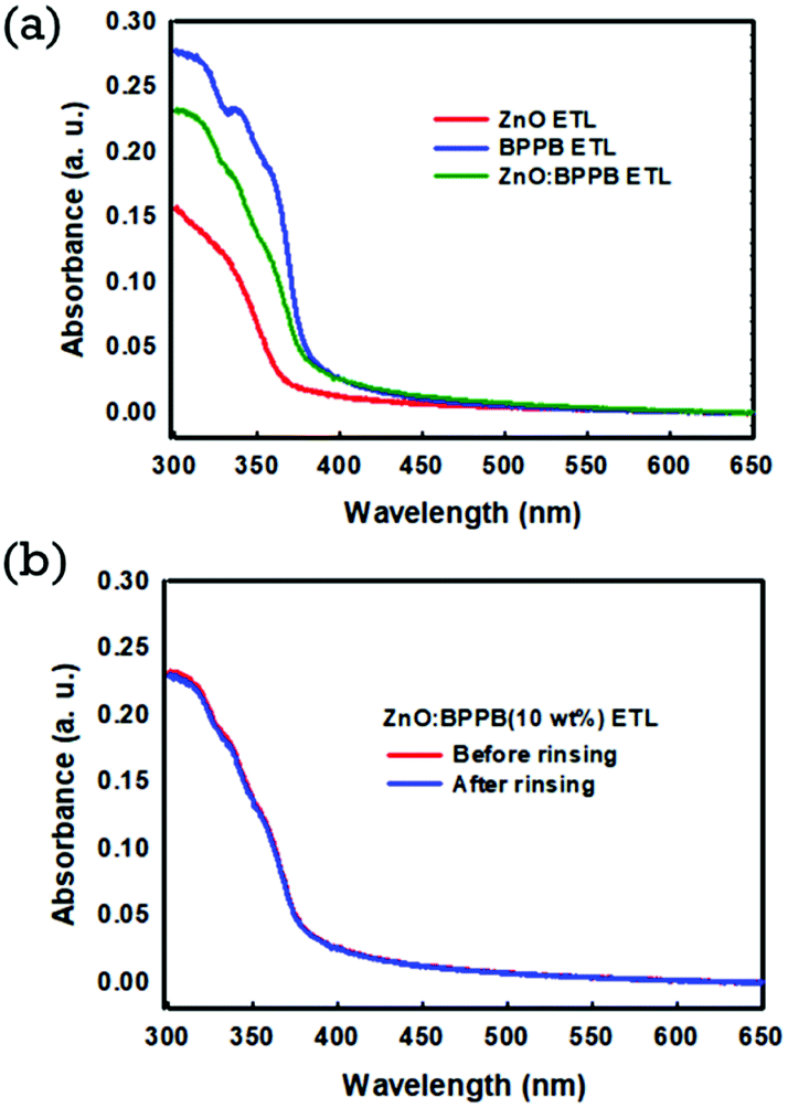 | ||
| Fig. 1 (a) UV-Vis absorption spectra of ZnO, BPPB SM and ZnO:BPPB (10 wt%) ETL films (b) UV-Vis absorption spectra of ZnO:BPPB (10 wt%) ETL films before and after rinsing with the octane solvent. | ||
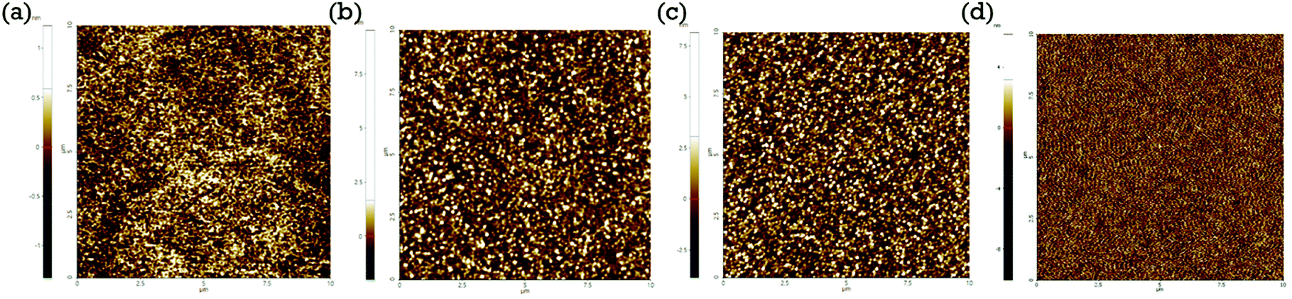 | ||
| Fig. 2 (a) The surface morphology of the sol–gel ZnO ETL, (b) ZnO/ZnO:BPPB (10 wt%), (c) ZnO/ZnO:BPPB (15 wt%), and (d) ZnO/ZnO:BPPB (20 wt%) interlayer films measured by AFM. | ||
Measured surface roughness slightly increases with increasing BPPB blending ratio. The low surface roughness values are suitable for subsequent QD layer coating. The ZnO:BPPB (20 wt%) interlayer shows relatively higher surface roughness, which may form a non uniform QD layer coating that creates leakage current paths in the device.18 In the literature, the device performances do not get influenced when the film roughness is less than 1.5 nm.18,24 The measured roughness of the ZnO:BPPB (15 wt%) film is 0.84 nm. So, we can expect that such a roughness value does not influence our device. In case of the ZnO:BPPB (20 wt%) film, the roughness is higher than 1.5 nm, which may affect the device performance as reported. The surface morphologies were analysed by SEM as shown in Fig. S5.† From the SEM images, the surface morphology of ZnO:BPPB films can be compared once more. The ZnO:BPPB (20 wt%) film shows a relatively non-uniform surface compared to other samples, which is consistent with the AFM data. The UPS measurement is carried out for the samples ZnO, ZnO:BPPB (10 wt%), ZnO:BPPB (15 wt%) and ZnO:BPPB (20 wt%) as shown in Fig. S6.†
With these different blended interlayers, inverted QLEDs were fabricated on patterned ITO. Sol–gel ZnO was used as the ETL, ZnO:BPPB as the interlayer and InP/ZnSe/ZnS QDs (InP-QDs) as the EML. The QLED device structure and energy band diagram are shown in Fig. 3(a) and (b). We used N-([1,1′-biphenyl]-4-yl)-N-(4-(dibenzo[b,d]-thiophen-2-yl)phenyl)dibenzo[b,d]thiophen-2-amine (DBTA), N-(1,1′-biphenyl-4-yl)-N-[4-(9-phenyl-9H-carbazol-3-yl)phenyl]-9,9-dimethyl-9H-fluoren-2-amine (PCBBiF)31 as hole transport layers (HTLs), 1,4,5,8,9,11-hexaazatriphenylenehexcarbonitrile (HATCN) as the hole injection layer (HIL) and aluminium (Al) as the anode. The effect of the ZnO:BPPB interlayer on the device performance was analysed. The thickness of the interlayer is kept constant around 15 nm, which is confirmed by ellipsometry and detailed explanation is given in the Experimental section. The device without (w/o) the interlayer (ZnO ETL as the control device) and ZnO:BPPB interlayer devices with different blending ratios are shown in Fig. 3(c–e). From the current density–voltage (J–V) characteristics of the devices, the device without the interlayer shows a higher current density but blended ZnO:BPPB interlayers showed a decreased current density. In detail, the device with the ZnO:BPPB (10 wt%) interlayer shows an increased driving voltage of 3.9 V compared to the device without the interlayer, which is 3.2 V. With higher blending ratios of BPPB in ZnO, the ZnO:BPPB (15 wt%) interlayer shows a higher driving voltage of 4.4 V compared to the ZnO:BPPB (10 wt%) interlayer. The driving voltage still further increased to 5.5 V with the ZnO:BPPB (20 wt%) interlayer. The current density of QLEDs gradually decreases as the BPPB blending ratios in ZnO increases from 10 wt% to 20 wt%. The ZnO:BPPB interlayer tends to slow down the electron injection due to the low electron mobility of the BPPB ETL and shallow LUMO energy level. Similarly, the maximum luminance of the devices was also decreased with the current density. The turn-on voltage (Von) of the devices without the interlayer, and with ZnO:BPPB (10 wt%), ZnO:BPPB (15 wt%) and ZnO:BPPB (20 wt%) interlayers are 1.8, 2.0, 2.0 and 2.1 V respectively. The ZnO:BPPB (15 wt%) interlayer device shows a 16.7% external quantum efficiency (EQE) is higher than without an interlayer device. This efficiency improvement suggests balanced carrier transport in the QD EML, which enhances the radiative recombination due to reduced electron injection. The device with the ZnO:BPPB (10 wt%) interlayer shows a lower EQE compared to that with ZnO:BPPB (15 wt%). And also the ZnO:BPPB (20 wt%) interlayer shows the maximum CE and EQE values of 15.1 cd A−1 and 15.4%. These maximum CE and EQE values are relatively low compared to those of the ZnO:BPPB (15 wt%) interlayer. We believe that higher concentrations of the BPPB ETL deteriorate the device performances by limited charge injection or by poor film surface roughness. The small molecule ETL exhibits low mobility at a higher current density. Therefore, efficiency roll-off is high in the high luminance region, however measured efficiency at 10–3000 cd m−2 is very high due to good charge balance. The ZnO:BPPB (15 wt%) interlayer was an optimal option to improve the performance of devices. To check the performance reproducibility of the device with the ZnO:BPPB (15 wt%) interlayer, we fabricated 18 devices. The histogram of maximum EQE values for 18 devices is shown in Fig. 3(f), where the average maximum EQE value obtained is 15.6%, demonstrating good reproducibility. The normalized electroluminescence (EL) spectra of the devices without and with the interlayer are shown in Fig. S7(b).† All the devices showed an EL peak at 632 nm without any parasitic emission. The device performances are summarized above in Table 1. The influence of the ZnO:BPPB interlayer was checked by using the electron-only device (EOD). The following are the device structures of EODs and HOD.
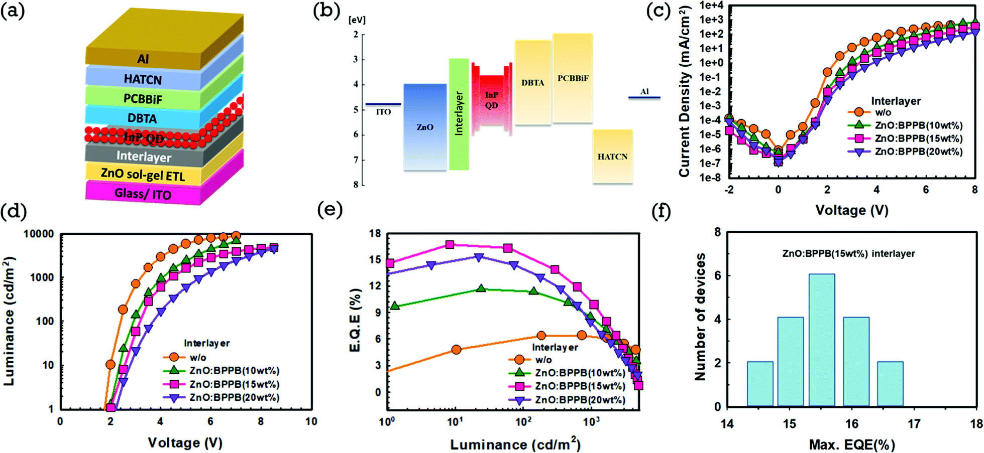 | ||
| Fig. 3 (a) QLED device structure (b) energy band diagram (c) current density versus voltage (J–V) characteristics (d) Luminance versus voltage (L–V) characteristics (e) EQE versus luminance characteristics of devices without (w/o) and with interlayers and (f) maximum EQE histogram of the 18 devices fabricated with the ZnO:BPPB (15 wt%) interlayer. | ||
| Interlayer | Turn-on voltage (Von) @ 1 cd m−2 | Driving voltage (V) @ 1000 cd m−2 | Maximum current efficiency (cd A−1) | Maximum EQE (%) (@ luminance (cd m−2)) | EQE (%) @ 100 cd m−2 | Maximum luminance (cd m−2) | CIE 1931 |
|---|---|---|---|---|---|---|---|
| w/o | 1.8 | 3.2 | 6.3 | 6.5 @ 717 | 5.9 | 8892 | (0.68, 0.32) |
| ZnO:BPPB (10 wt%) |
2.0 | 3.9 | 11.4 | 11.6 @ 24 | 11.4 | 6844 | (0.68, 0.32) |
| ZnO:BPPB (15 wt%) |
2.0 | 4.4 | 16.4 | 16.7 @ 9 | 15.6 | 4878 | (0.68, 0.32) |
| ZnO:BPPB (20 wt%) |
2.1 | 5.5 | 15.1 | 15.4 @ 22 | 14.0 | 4689 | (0.68, 0.32) |
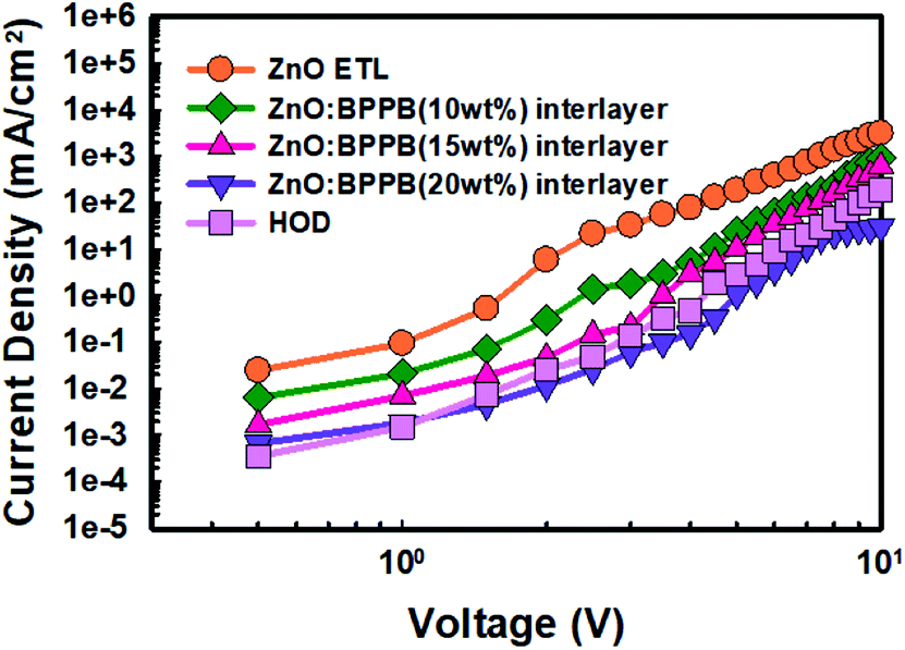
EOD 1: ITO/ZnO/QD/LiF/Al.
EOD 2: ITO/ZnO/ZnO:BPPB (10 wt%) interlayer/QD/LiF/Al.
EOD 3: ITO/ZnO/ZnO:BPPB (15 wt%) interlayer/QD/LiF/Al.
EOD 4: ITO/ZnO/ZnO:BPPB (20 wt%) interlayer/QD/LiF/Al.
HOD:ITO/PEDOT:PSS/QD/DBTA/PCBBiF/HATCN/Al.
The J–V characteristics of EODs and HOD are shown in Fig. 4. The EOD device without the interlayer (sol–gel ZnO ETL) shows a higher current density than the HOD device, which results in severe charge imbalance in the device. The devices with the ZnO:BPPB interlayer show a remarkably lower electron current density. In the EOD device with the ZnO:BPPB (10 wt%) interlayer, the current density relatively decreased than ZnO ETL current density. Whereas with ZnO:BPPB (15 wt%) interlayer, the current density significantly reduced and almost matched with the HOD device. With the ZnO:BPPB (20 wt%) interlayer, the current density decreases, even more, showing a crossing point with the HOD device.35 This indicates that the ZnO:BPPB (20 wt%) interlayer shows relatively poor charge balance compared with the ZnO:BPPB (15 wt%) interlayer. On blending higher weight ratios of BPPB in ZnO, the device performance deteriorates due to too much slow charge injection from ZnO into the QD EML. With optimum doping of the BPPB ETL (15 wt%) in ZnO, charge balance was improved with enhanced device performances. The decrease of the electron current density is due to slower electron mobility of the BPPB SM ETL and shallow LUMO energy level. This shallow energy level of the BPPB ETL seems to create a large injection barrier at the QD EML interface.
 | ||
| Fig. 4
J–V characteristics of EODs with the sol–gel ZnO ETL, ZnO:BPPB (10 wt%), ZnO:BPPB (15 wt%), and ZnO:BPPB (20 wt%) interlayers and the HOD. | ||
To further confirm if the ZnO:BPPB interlayer slows down the ZnO ETL mobility, the space charge limited current (SCLC) mobility was calculated using the Mott–Gurney law.36 The calculated mobilities for ZnO, ZnO:BPPB (10 wt%), ZnO:BPPB (15 wt%), ZnO:BPPB (20 wt%), and the HOD were 5.2 × 10⁻⁴ cm2 V−1 s−1, 1.9 × 10⁻⁵ cm2 V−1 s−1, 5.5 × 10⁻⁵ cm2 V−1 s−1, 3.2 × 10⁻⁶ cm2 V−1 s−1 and 8.69 × 10⁻⁶ cm2 V−1 s−1. The ETL mobilities were decreased with increasing BPPB blending ratio in ZnO. The ZnO:BPPB (20 wt%) ETL shows much slower mobility compared to HOD mobility. Therefore, ZnO:BPPB (15 wt%) shows better device efficiency.
To study the effect of the ZnO:BPPB interlayer on the emission of InP-QDs, we measured the time-resolved photoluminescence (TRPL) decay curves as shown in Fig. 5(a). The structure of fabricated samples and their average exciton decay lifetimes are summarized in Table S1,† where all the samples are excited by using a 340 nm monochromatic light source. The exciton lifetime of the glass/QD sample was 28.3 ns, but the sample with the glass/ZnO/QD film showed a shorter exciton lifetime of 23.2 ns. This implies that, when the QDs were in direct contact with the ZnO ETL, a strong interface exciton quenching was observed due to the interface charge transfer process.24,32,33 By insertion of the ZnO:BPPB (10 wt%) interlayer between ZnO and QDs, the exciton lifetime improved from 23.2 ns to 25.7 ns. The ZnO:BPPB (15 wt%) interlayer sample shows a relatively longer exciton lifetime of 27.2 ns than that of the ZnO:BPPB (10 wt%) interlayer. This indicates that the improved exciton lifetime is due to the suppressed interfacial charge transfer because of the shallow LUMO of the BPPB ETL. With the ZnO:BPPB (20 wt%) interlayer, the exciton lifetime decreased to 26.1 ns which showed a downtrend. This demonstrates that the defect states in the high surface roughness film act as quenching sites. We also performed the PL measurement with and without interlayers, as shown in Fig. 5(b). The PL intensities of the samples with the interlayers are increased, which showed a similar trend to TRPL data. Therefore, appropriate blending ratios of BPPB into ZnO can enhance the device performance not only by reducing the electron injection but also by suppressing the exciton quenching of InP-QDs. The measured film PLQY of QD samples with ZnO and ZnO:BPPB interlayers is shown in Table S2.† From the interface quenching analysis and film PLQY analysis, the PLQY improvement is around 20%. The overall enhanced device efficiency is 2.57 times. Therefore, the efficiency improvement by blocking interface quenching is a minor factor for the total enhancement. Based on this, we conclude that the charge balance is a major factor for the enhancement of device efficiency. Finally, the operational lifetime of inverted red devices without and with the ZnO:BPPB (15 wt%) interlayer was analysed as shown in Fig. 6. The device with the ZnO:BPPB (15 wt%) interlayer shows a half lifetime (T50) of ∼595 hours at an initial luminance of 1000 cd m−2. The device lifetime can be calculated as L0nT50 = constant, where L0 is the initial luminance, n is the acceleration factor and T50 is the half lifetime. In the literature for inverted QLED devices, the acceleration factor (n) of the device lifetime is near to ∼1.8.31,34,37 The half lifetime (T50) of the ZnO:BPPB (15 wt%) interlayer device, at an initial luminance of 100 cd m−2 is calculated to be ∼37542 hours. The enhancement in device efficiency contributes to improvement of the device lifetime. Generally, in the QLED device, charge imbalance leads to QD charging, non-radiative auger recombination and joule heating which degrades the device stability.38,39 Using ZnO:BPPB as an interlayer improves the charge balance in the QLED device which results in significant improvement of device efficiency. As shown by the results, excellent device lifetime was achieved by reducing QD charging and non-radiative auger recombination. In addition, reduced interfacial quenching may contribute as a minor factor for the lifetime enhancement. In conclusion, the improvement in efficiency and lifetime is achieved by matching the charge balance and suppressing the interfacial exciton quenching of InP-QDs.
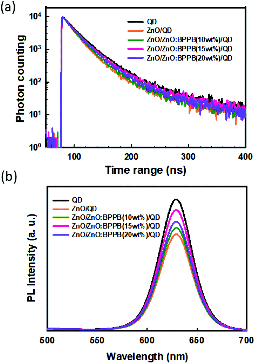 | ||
| Fig. 5 (a) Time-resolved photoluminescence (TRPL) curves and (b) PL intensities of the samples glass/QD, glass/ZnO/QD, glass/ZnO/ZnO:BPPB (10 wt%)/QD, glass/ZnO/ZnO:BPPB (15 wt%)/QD, and glass/ZnO/ZnO:BPPB (20 wt%)/QD. | ||
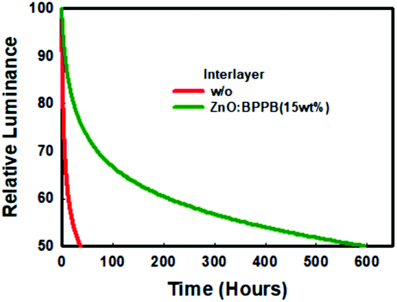 | ||
| Fig. 6 Lifetime of devices without and with the ZnO:BPPB (15 wt%) interlayer. | ||
Experimental
InP-QD and sol–gel ZnO ETL preparation
InP/ZnSe/ZnS, core/shell/shell type QDs were prepared according to the previously reported approach shown in our previous work.35 To prepare the sol–gel ZnO precursor solution, we dissolved 0.5 M zinc acetate dihydrate and monoethanolamine in 2-methoxyethanol. The solution was stirred for 3 hours at 60 °C.QLED fabrication
The ITO substrates were cleaned using acetone and isopropyl alcohol in an ultrasonic bath for 10 min and washed with deionized water. On ITO substrates, sol–gel ZnO was spin-coated at 3000 rpm for 60 s and annealed for 60 min at 150 °C. The BPPB SM ETL blended ZnO was prepared by adding different weight ratios of BPPB into ZnO in a mixed solvent of 2-methoxyethanol and chlorobenzene (1:2 vol) and stirred for 2 hours at 60 °C. To get the same desired thickness of ZnO:BPPB with different doping concentrations, spin-coating rpm was varied. Then the prepared solution of ZnO:BPPB (10 wt%), (15 wt%), and (20 wt%) was spin-coated on the sol–gel ZnO film at 3000, 3500, and 4000 rpm for 60 s and annealed at 150 °C for 30 min. The thickness of the interlayer is around ∼15 nm, respectively. The total thickness of the ETL is kept constant at around 60 nm. Afterward, red InP/ZnSe/ZnS QDs with a concentration of 8 mg ml−1 in octane were spin-coated at 3000 rpm for 30 s. DBTA (10 nm) and PCBBiF (33 nm) as HTLs and HATCN (7 nm) as the HIL were thermally evaporated at a rate of 0.3–0.5 A° s−1. The Al (100 nm) anode was thermally evaporated under a pressure of 6 × 10⁻⁸ Torr. The emitting area was 2 × 2 mm2.
Characterization
The QLED device characteristics, J–V and L–V, were measured using a Konica Minolta CS-100A with luminance and color meters. The electroluminescence (EL) spectra, efficiency and Commission Internationale de l'Eclairage (CIE) 1931 color coordinates were obtained with a spectroradiometer (Konica Minolta CS-2000A). The TRPL measurements were performed with a Quantaurus-Tau fluorescence lifetime measurement system (C11367-03, Hamamatsu Photonics Co.). A UV-Visible spectrophotometer (JASCO, S-4100) was used to measure absorbance. By using a spectroscopic ellipsometer (HORIBA), all the film thicknesses were measured.Conclusions
We report a simple and efficient strategy by modulating the electron transport in inverted red cadmium-free QLED devices using organic and inorganic hybrid interlayers. By insertion of a thin interlayer, the electron mobility of the ZnO ETL reduces and charge balance in the QLED device is enhanced. The organic and inorganic hybrid interlayer not only delays the electron flow to match charge balance in the EML but also suppresses the interfacial exciton quenching between the ZnO layer and QD EML. The device with the ZnO:BPPB (15 wt%) interlayer shows 16.7% EQE. In addition, the device shows a half lifetime (T50) of ∼595 hours at 1000 cd m−2. We believe that the organic and inorganic hybrid interlayer approach is an easy method to attain high-performance QLEDs.
Conflicts of interest
There are no conflicts to declare.Acknowledgements
This research work was supported by the Technology Innovation Program (20010737) funded by the Ministry of Trade, Industry and Energy (MOTIE, Korea).Notes and references
- Y. Shirasaki, G. J. Supran, M. G. Bawendi and V. Bulović, Emergence of Colloidal Quantum-Dot Light-Emitting Technologies, Nat. Photonics, 2013, 7, 13–23 CrossRef CAS.
- X. Dai, Y. Deng, X. Peng and Y. Jin, Quantum-Dot Light-Emitting Diodes for Large-Area Displays: Towards the Dawn of Commercialization, Adv. Mater., 2017, 29, 1607022 CrossRef PubMed.
- M. K. Choi, J. Yang, T. Hyeon and D.-H. Kim, Flexible quantum dot light-emitting diodes for next-generation displays, npj Flexible Electron., 2018, 2, 10 CrossRef.
- Q. Yuan, T. Wang, P. Yu, H. Zhang, H. Zhang and W. Ji, A review on the electroluminescence properties of quantum-dot light-emitting diodes, Org. Electron., 2021, 90, 106086 CrossRef CAS.
- L. Kim, P. O. Anikeeva, S. A. Coe-Sullivan, J. S. Steckel, M. G. Bawendi and V. Bulovicì, Contact Printing of Quantum Dot Light-Emitting Devices, Nano Lett., 2008, 8, 4513 CrossRef CAS PubMed.
- Z. Yang, M. Gao, W. Wu, X. Yang, X. W. Sun, J. Zhang, H.-C. Wang, R.-S. Liu, C.-Y. Han, H. Yang and W. Li, Recent Advances in Quantum Dot-Based Light-Emitting Devices: Challenges and Possible Solutions, Mater. Today, 2019, 24, 69–93 CrossRef CAS.
- J. Lim, M. Park, W. K. Bae, D. Lee, S. Lee, C. Lee and K. Char, Highly Efficient Cadmium-Free Quantum Dot Light-Emitting Diodes Enabled by the Direct Formation of Excitons within InP@ZnSeS Quantum Dots, ACS Nano, 2013, 7, 9019–9026 CrossRef CAS PubMed.
- H. C. Wang, H. Zhang, H. Y. Chen, H. C. Yeh, M. R. Tseng, R. J. Chung, S. Chen and R. S. Liu, Cadmium-Free InP/ZnSeS/ZnS Heterostructure-Based Quantum Dot Light-Emitting Diodes with a ZnMgO Electron Transport Layer and a Brightness of Over 10000 cd m−2, Small, 2017, 13, 1603962 CrossRef PubMed.
- D. Li, B. Kristal, Y. Wang, J. Feng, Z. Lu, G. Yu, Z. Chen, Y. Li, X. Li and X. Xu, Enhanced Efficiency of InP-Based Red Quantum Dot Light-Emitting Diodes, ACS Appl. Mater. Interfaces, 2019, 11(37), 34067–34075 CrossRef CAS PubMed.
- C. Ippen, W. Guo, D. Zehnder, D. Kim, J. Manders, D. Barrera, B. Newmeyer, D. Hamilton, C. Wang, C. Hotz, R. Ma, J.-K. Bin, B. Kim, K. Kim, K. Jang, J. Park, T. Lee, W.-Y. Kim and J. Lee, High efficiency heavy metal free QD-LEDs for next generation displays, J. Soc. Inf. Disp., 2019, 27, 338 CrossRef CAS.
- Y. Li, X. Hou, X. Dai, Z. Yao, L. Lv, Y. Jin and X. Peng, Stoichiometry-Controlled InP-Based Quantum Dots: Synthesis, Photoluminescence, and Electroluminescence, J. Am. Chem. Soc., 2019, 141, 6448–6452 CrossRef CAS PubMed.
- Y.-H. Won, O. Cho, T. Kim, D.-Y. Chung, T. Kim, H. Chung, H. Jang, J. Lee, D. Kim and E. Jang, Highly efficient and stable InP/ZnSe/ZnS quantum dot light-emitting diodes, Nature, 2019, 575, 634–638 CrossRef CAS PubMed.
- Z. Wu, P. Liu, W. Zhang, K. Wang and X. W. Sun, Development of InP Quantum Dot-Based Light-Emitting Diodes, ACS Energy Lett., 2020, 5, 1095–1106 CrossRef CAS.
- Y.-Q. Liu, D.-D. Zhang, H.-X. Wei, Q.-D. Ou, Y.-Q. Li and J.-X. Tang, Highly efficient quantum-dot light emitting diodes with sol-gel ZnO electron contact, Opt. Mater. Express, 2017, 7, 2161–2167 CrossRef CAS.
- J. Pan, J. Chen, Q. Huang, Q. Khan, X. Liu, Z. Tao, Z. Zhang, W. Lei and A. Nathan, Size Tunable ZnO Nanoparticles to Enhance Electron Injection in Solution Processed QLEDs, ACS Photonics, 2016, 3, 215–222 CrossRef CAS.
- E. Moyen, J. H. Kim, J. Kim and J. Jang, ZnO Nanoparticles for Quantum-Dot-Based Light-Emitting diodes, ACS Appl. Nano Mater., 2020, 3(6), 5203–5211 CrossRef CAS.
- X. Dai, Z. Zhang, Y. Jin, Y. Niu, H. Cao, X. Liang, L. Chen, J. Wang and X. Peng, Solution-processed, high-performance light-emitting diodes based on quantum dots, Nature, 2014, 515, 96–99 CrossRef CAS PubMed.
- K. Ding, H. Chen, L. Fan, B. Wang, Z. Huang, S. Zhuang, B. Hu and L. Wang, Polyethylenimine Insulativity-Dominant Charge-Injection Balance for Highly Efficient Inverted Quantum Dot Light-Emitting Diodes, ACS Appl. Mater. Interfaces, 2017, 9, 20231–20238 CrossRef CAS PubMed.
- C. Y. Lee, N. N. Mude, R. Lampande, K. J. Eun, J. E. Yeom, H. S. Choi, S. H. Sohn, J. M. Yoo and J. H. Kwon, Efficient Cadmium Free Inverted Red Quantum Dot Light-Emitting Diodes, ACS Appl. Mater. Interfaces, 2019, 11, 36917–36924 CrossRef CAS PubMed.
- M. Chrzanowski, M. Kuchowicz, R. Szukiewicz, P. Sitarek, J. Misiewicz and A. Podhorodecki, Enhanced efficiency of quantum dot light-emitting diode by sol-gel derived Zn1–xMgxO electron transport layer, Org. Electron., 2020, 80, 105656 CrossRef CAS.
- Y. Lee, B. G. Jeong, H. Roh, J. Roh, J. Han, D. C. Lee, W. K. Bae, J.-Y. Kim and C. Lee, Enhanced Lifetime and Efficiency of Red Quantum Dot Light-Emitting Diodes with Y-Doped ZnO Sol–Gel Electron-Transport Layers by Reducing Excess Electron Injection, Adv. Quantum Technol., 2018, 1, 1700006 CrossRef.
- S. Cao, J. Zheng, J. Zhao, Z. Yang, C. Li, X. Guan, W. Yang, M. Shang and T. Wu, Enhancing the performance of Quantum Dot Light-Emitting Diodes Using Room-Temperature-Processes Ga-Doped ZnO Nanoparticles as the electron transport Layer, ACS Appl. Mater. Interfaces, 2017, 9, 15605–15614 CrossRef CAS PubMed.
- Y. Sun, W. Wang, H. Zhang, Q. Su, J. Wei, P. Liu, S. Chen and S. Zhang, High-Performance Quantum Dot Light-Emitting Diodes Based on Al-Doped ZnO Nanoparticles Electron Transport Layer, ACS Appl. Mater. Interfaces, 2018, 10(22), 18902–18909 CrossRef CAS PubMed.
- J. Pan, C. Wei, L. Wang, J. Zhuang, Q. Huang, w. Su, Z. Cui, A. Nathan, W. Lei and J. Chen, Boosting the efficiency of inverted quantum dot light-emitting diodes by balancing charge densities and suppressing exciton quenching through band alignment, Nanoscale, 2018, 10, 592 RSC.
- K. Sun, F. Li, Q. Zeng, H. Hu and T. Guo, Blue quantum dot light emitting diodes with polyvinylpyrrolidone-doped electron transport layer, Org. Electron., 2018, 63, 65–70 CrossRef CAS.
- B. Liu, L. Lan, Y. Liu, H. Tao, H. Li, H. Xu, J. Zou, M. Xu, L. Wang, J. Peng and Y. Cao, Improved performance of quantum dot light-emitting diodes by hybrid electron transport layer comprised of ZnO nanoparticles doped organic small molecule, Org. Electron., 2019, 74, 144–151 CrossRef CAS.
- J.-W. Jou, S. Kumar, A. Agarwal, T.-H. Li and S. Sahoo, Approaches for fabricating high efficiency organic light emitting diodes, J. Mater. Chem. C, 2015, 3, 2974–3002 RSC.
- Y. J. Kang, S. H. Han and J. Y. Lee, Lifetime enhancement of blue thermally activated delayed fluorescent devices by separated carrier channels using dibenzofuran-triazine type hosts, J. Ind. Eng. Chem., 2018, 62, 258–264 CrossRef CAS.
- S. K. Kim, M. J. Park, R. Pode and J. H. Kwon, A Deep Blue Strong Microcavity Organic Light-Emitting Diode Optimized by a Low absorption Semitransparent Cathode and a Narrow Bandwidth Emitter, Advanced Photonics Research, 2021, 2, 2000122 CrossRef.
- E. G. Lee, C. Y. Yang, W. J. Chung and J. Y. Lee, CN decoration of dibenzofuran modified biphenyl for high triplet energy host for blue phosphorescent organic light-emitting diodes, Org. Electron., 2021, 89, 106037 CrossRef CAS.
- J. E. Yeom, D. H. Shin, R. Lampande, Y. H. Jung, N. N. Mude, J. H. Park and J. H. Kwon, Good Charge Balanced Inverted Red InP/ZnSe/ZnS-Quantum Dot Light Emitting Diode with New High Mobility and Deep HOMO Level Hole Transport Layer, ACS Energy Lett., 2020, 5, 3868–3875 CrossRef CAS.
- X. Yang, Z. Zhang, T. Ding, N. Wang, G. Chen, C. Dang, H. V. Demir and X. W. Sun, High-efficiency all-inorganic full-colour quantum dot light-emitting diodes, Nano Energy, 2018, 46, 229–233 CrossRef CAS.
- H. Zang and S. Chen, An ZnMgO:PVP inorganic–organic hybrid electron transport layer: towards efficient bottom-emission and transparent quantum dot light-emitting diodes, J. Mater. Chem. C, 2019, 7, 2291 RSC.
- Y. Cun, C. Mai, Y. Luo, L. Mu, J. Li, L. Cao, D. Yu, M. Li, B. Zhang, H. Li and J. Wang, All-solution processed high performance inverted quantum dot light emitting diodes, J. Mater. Chem. C, 2020, 8, 4264 RSC.
- S. Kim, H. Yang and Y. Kim, controlling of carrier injection and transport in quantum dot light emitting diodes (QLEDs) via modulating Schottky injection barrier and carrier mobility, J. Appl. Phys., 2019, 126, 185702 CrossRef.
- H. Moon, W. Lee, J. Kim, D. Lee, S. Cha, S. Shin and H. Chae, Composition-tailored ZnMgO nanoparticles for electron transport layers of highly efficient and bright InP-based quantum dot light emitting diodes, Chem. Commun., 2019, 55, 13299 RSC.
- D. S. Chung, T. Davidson-Hall, H. Yu, F. Samaeifar, P. Chun, Q. Lyu, G. Cotella and H. Aziz, Significant enhancement in quantum-dot light emitting device stability via a ZnO:polyethylenimine mixture in the electron transport layer, Nanoscale Adv., 2021, 3, 5900 RSC.
- F. Wang, W. Sun, P. Liu, Z. Wang, J. Zhang, J. Wei, Y. Li, T. Hayat, A. Alsaedi and Z. Tan, Achieving Balanced Charge Injection of Blue Quantum Dot Light-Emitting Diodes through Transport Layer Doping Strategies, J. Phys. Chem. Lett., 2019, 10(5), 960–965 CrossRef CAS PubMed.
- H. Moon, C. Lee, W. Lee, J. Kim and H. Chae, Stability of Quantum Dots, Quantum Dot Films, and Quantum Dot Light-Emitting Diodes for Display Applications, Adv. Mater., 2019, 31, 1804294 CrossRef PubMed.
Footnote |
| † Electronic supplementary information (ESI) available. See DOI: 10.1039/d1na00716e |
| This journal is © The Royal Society of Chemistry 2022 |