
 Open Access Article
 This Open Access Article is licensed under a Creative Commons Attribution-Non Commercial 3.0 Unported Licence
Localized thermal spike driven morphology and electronic structure transformation in swift heavy ion irradiated TiO2 nanorods†
Sutapa
Dey
 a,
Anusmita
Chakravorty
b,
Shashi Bhusan
Mishra
c,
Nasima
Khatun
a,
Arnab
Hazra
d,
Birabar Ranjit Kumar
Nanda
c,
Chandran
Sudakar
e,
Debdulal
Kabiraj
b and
Somnath C.
Roy
*a
a,
Anusmita
Chakravorty
b,
Shashi Bhusan
Mishra
c,
Nasima
Khatun
a,
Arnab
Hazra
d,
Birabar Ranjit Kumar
Nanda
c,
Chandran
Sudakar
e,
Debdulal
Kabiraj
b and
Somnath C.
Roy
*a
aSemiconducting Oxide Materials, Nanostructures and Tailored Heterojunction (SOMNaTH) Lab, Functional Oxide Research Group (FORG), Department of Physics, Indian Institute of Technology Madras, Chennai 600036, India. E-mail: somnath@iitm.ac.in
bInter-University Accelerator Centre, Aruna Asaf Ali Marg, New Delhi 110067, India
cCondensed Matter Theory and Computational Lab, Department of Physics and Center for Atomistic Modelling and Materials Design (CAMMD), Indian Institute of Technology Madras, Chennai 600036, India
dDepartment of Electrical & Electronics Engineering, Birla Institute of Technology & Science-Pilani, Pilani Campus, Pilani-333031, Rajasthan, India
eMultifunctional Materials Laboratory, Department of Physics, Indian Institute of Technology Madras, Chennai 600036, India
First published on 15th November 2021
Abstract
Irradiation of materials by high energy (∼MeV) ions causes intense electronic excitations through inelastic transfer of energy that significantly modifies physicochemical properties. We report the effect of 100 MeV Ag ion irradiation and resultant localized (∼few nm) thermal spike on vertically oriented TiO2 nanorods (∼100 nm width) towards tailoring their structural and electronic properties. Rapid quenching of the thermal spike induced molten state within ∼0.5 picosecond results in a distortion in the crystalline structure that increases with increasing fluences (ions per cm2). Microstructural investigations reveal ion track formation along with a corrugated surface of the nanorods. The thermal spike simulation validates the experimental observation of the ion track dimension (∼10 nm diameter) and melting of the nanorods. The optical absorption study shows direct bandgap values of 3.11 eV (pristine) and 3.23 eV (5 × 10¹² ions per cm2) and an indirect bandgap value of 3.10 eV for the highest fluence (5 × 10¹³ ions per cm2). First principles electronic structure calculations corroborate the direct-to-indirect transition that is attributed to the structural distortion at the highest fluence. This work presents a unique technique to selectively tune the properties of nanorods for versatile applications.
1. Introduction
Manipulation of physical and chemical properties of materials through modification of crystallinity, morphology and electronic structure is of great interest to researchers.1,2 High energy ion beam irradiation is a unique technique, which induces localized modification in a material without the irradiating ions being implanted or doped into the lattice.3–6 When an energetic ion travels through a material, it transfers its energy to the atomic and electronic subsystems in two ways, which are called nuclear/elastic energy loss (Sn) and electronic/inelastic energy loss (Se). In general, if the energy of an ion exceeds 1 MeV per nucleon, it is called the swift heavy ion (SHI), where Se dominates over Sn. When Se becomes larger than a threshold value, the huge energy deposited by an ion creates a latent track along its trajectory with a cross-section of a few nanometers.7 The track is a region of distinguishable crystallinity depending on the type of target material, ion energy, and the type of ion chosen. Thus, SHI irradiation provides flexibility to selectively modify the target material in a highly localized manner.Titanium dioxide (TiO2) remains one of the most prominent members of the metal oxide family owing to its high chemical and thermal stability, excellent photoactivity, biocompatibility and availability in the form of three different polymorphs (anatase, brookite and rutile).8,9 There are a few reports, which have discussed SHI irradiation-induced structural changes in TiO2, for example, from amorphous to anatase,10 rutile,11,12 and mixed-phase;12 and anatase to amorphous,13 rutile,14 and mixed-phase15 transformations. SHI irradiation induced effects have also been studied on doped TiO2. For example, Gautam et al.16 reported 120 MeV Ag and 130 MeV Ni ion induced phase transformation in undoped and niobium doped anatase TiO2 composite thin films. Thakurdesai et al. observed a SHI-induced phase transition of a pulsed laser deposited TiO2 thin film from the rutile to the anatase phase.17 SHI-induced nano or microlithography18–21 has been reported on single crystal rutile TiO2. Further, formation of the ion track under SHI irradiation has been investigated in single crystal rutile TiO2 with (001),22,23 (110),24–26 and (100)27 orientations. Latent tracks of different morphologies such as cylindrical, dumbbell-shaped or sandglass-like have been observed with variation of ion path length as a consequence of molten phase outflow and recrystallization.28 In the case of thin films, 120 MeV Ag ion irradiation has been performed on a rutile TiO2 film deposited by ion beam sputtering on silicon to investigate the influence of SHI irradiation on the dynamics of phonon interactions.29 Rath et al. reported 79 MeV Br ion induced modifications in a 200 nm thick rutile TiO2 thin film prepared by DC magnetron sputtering on a Si (100) substrate.30 The sample crystallinity was retained up to a fluence of 1 × 10¹³ ions per cm2, even though the Se value exceeded the threshold for amorphization along the ion track in TiO2.30 Some of the important published studies on Ag ion irradiation effects on TiO2 are listed in Table T1 (ESI†). It is therefore apparent that several studies have been reported on SHI irradiation of TiO2 single-crystal and thin films; however, such studies on TiO2 nanostructures remain unexplored.
One-dimensional nanostructures such as nanowires and nanorods, offer the advantage of unidirectional charge transport along with high specific surface area.31 Particularly, highly aligned and vertically oriented TiO2 nanorods hydrothermally grown on a fluorine doped tin oxide (FTO) coated glass substrate have shown strong potential in applications such as electrode materials with a transparent conducting window for solar cells,32 water splitting,33 electrocatalysis,34 bio-photoelectrochemical reactions,35 UV photodetectors,36 electron transport layers in perovskite solar cells,37 electron injection layers in DSSCs,38 sensors,39etc. In addition, the single-crystalline nature of each nanorod provides a long-range periodicity throughout the individual nanorod structure, which is a suitable platform for the study of irradiation effects. Moreover, a small lateral dimension (a few tens of nanometers) of the nanorods provides limited space for thermal energy transfer and atomic displacement in the radial direction. Therefore, it is interesting to explore the effect of SHI irradiation-induced localized energy transfer in rutile TiO2 nanorods. Here, we present the crystalline phase, morphology and electronic structure transformation of the SHI (100 MeV Ag ion) irradiated TiO2 nanorods, and their effect on the optical absorption. The experimental data and observation are correlated with the thermal spike model-based analysis and density functional theory (DFT) calculated band structure to gain an insight into ion beam-induced disorder and defects in these nanorods.
2. Experimental section
2.1. Preparation of TiO2 nanorod arrays
TiO2 nanorod arrays were synthesized by a hydrothermal method on a FTO coated glass substrate. The details of the synthesis process are given in our previous report.40 Briefly, the hydrothermal process was carried out at 200 °C for 2 hours, where the reaction solution comprised 10 ml of concentrated hydrochloric acid (HCl 37%), 10 ml of de-ionized (DI) water, and 0.3 ml of titanium(IV) butoxide. The as-prepared TiO2 nanorod samples were rinsed thoroughly with DI water, air-dried, and finally annealed at 450 °C for 30 minutes to ensure the stability of TiO2 nanorods on the substrate.2.2. Experimental details of ion irradiation
The TiO2 nanorods grown on a FTO coated glass substrate were irradiated at room temperature with 100 MeV Ag ions using the 15UD accelerator at the Inter-University Accelerator Centre, New Delhi, India.41 The fluences used for irradiation were 1 × 10¹², 5 × 10¹², 1 × 10¹³ and 5 × 10¹³ ions per cm2. The beam current was maintained at ∼7 nA to avoid any joule heating. The Stopping and Range of Ions in Matter (SRIM)42 code was used to calculate the electronic energy loss and range of the ion inside the material.2.3. Characterization
A field emission scanning electron microscope (FESEM) (Model-FEI Inspect F50), operating at 30 keV, was employed to study the surface morphology. X-ray diffraction (XRD) patterns were recorded using a RigakuSmartLab X-ray Diffractometer with Cu Kα (λ = 0.154 nm), operating at 45 kV and 200 mA anode current. Raman spectroscopy was performed using the HORIBA LabRAM HR instrument equipped with an argon ion laser emitting 488 nm (2.54 eV) excitation wavelength. A transmission electron microscope (TEM) (Model-Tecnai G2 T20), operating at an accelerating voltage of 200 kV, was used to observe the microstructure and record the electron diffraction pattern. An X-ray photoelectron spectrometer (ESCAprobe TPD), equipped with an Mg Kα X-ray source, was employed to perform X-ray photoelectron spectroscopy (XPS). Optical absorption spectroscopy was carried out using a PerkinElmer LAMBDA 950 UV-Vis-NIR Spectrophotometer, equipped with an integrating sphere accessory, and operating in diffuse reflectance mode. Photoluminescence (PL) spectra were acquired using a JobinYvonFluorimeter (Fluorolog-3-11), equipped with a Xe lamp source and a photomultiplier tube detector.3. Results and discussion
3.1. Morphology, crystallinity, microstructure and chemical composition analysis
The surface morphologies of the pristine and irradiated TiO2 nanorod arrays investigated through FESEM images are presented in Fig. 1. The pristine TiO2 nanorods are shown in Fig. 1(a). It is observed that the individual rods are tetragonal in shape with a length of ∼1 μm and an average width of ∼100 nm. The surface morphologies of the samples after irradiation at different fluences (1 × 10¹², 5 × 10¹², 1 × 10¹³ and 5 × 10¹³ ions per cm2) are shown in Fig. 1(b), (c), (d) and (e) respectively. The range of 100 MeV Ag in TiO2 (density 4.25 g cm−3), estimated using the SRIM code,42 is 8.85 μm, which ensures that all irradiating ions pass through the nanorod structure (∼1 μm long) without being implanted or doped in the material.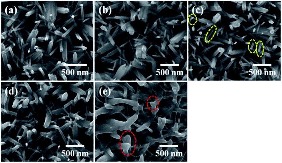 | ||
| Fig. 1 FESEM images of (a) pristine and irradiated samples with (b) 1 × 10¹², (c) 5 × 10¹², (d) 1 × 10¹³ and (e) 5 × 10¹³ ions per cm2 fluences. Yellow ellipses in (c) indicate slight bending of nanorods, and red ellipses in (e) indicate interconnected adjacent nanorods. | ||
At a low fluence of 1 × 10¹² ions per cm2, no significant changes are observed (Fig. 1(b)). However, the nanorod structures show slight bending at a few locations (Fig. 1(c)) after irradiation at a fluence of 5 × 10¹² ions per cm2 (indicated by yellow ellipses), followed by an increase in bending and morphological distortion at a fluence of 1 × 10¹³ ions per cm2 (Fig. 1(d)). Further increase of fluence to 5 × 10¹³ ions per cm2 causes a significant structural distortion and bending of individual nanorods with the appearance of a semi-transparent layer connecting the adjacent rods (Fig. 1(e)). The interconnected adjacent nanorods are indicated by red ellipses in Fig. 1(e). It appears that the energy transferred from an incident ion to a nanorod induces intense local heating leading to melting and bending of the TiO2 nanorods. Diffusion of the molten material between adjacent nanorods results in the formation of such interconnecting layers. Here, the individual nanorods having lateral dimensions of ∼100 nm provide limited space for heat dissipation and molten state flow. Therefore, as a result of thermal spike induced melting, significant morphological changes are clearly observed from the FESEM images. However, in the case of polycrystalline films even if a thermal spike induced change in crystallinity occurs, it would not be so clearly evident through morphological changes. The digital photographs of actual samples irradiated at different fluences are shown in the ESI (Fig. S1†).
To investigate the structural changes induced by SHI irradiation, XRD analysis was carried out for pristine and irradiated samples, and the results are presented in Fig. 2(a). The XRD pattern of the pristine sample shows peaks at 36.10°, 41.33°, 54.59°, 62.93° and 68.99°, which correspond to (101), (111), (211), (002) and (301) of rutile TiO2 (ICSD reference code 01-073-1765) respectively. The additional peaks are attributed to SnO2 (ICSD reference code 01-077-0452) from the FTO coating of the substrate. After irradiation, there is a gradual reduction in crystallinity as indicated by decreasing intensities for (101), (211), and (002) peaks. To analyze the shift in the position of the peaks, a high-resolution X-ray scan was carried out for the (101) and (211) planes and the data are presented in Fig. 2(b) and (c), respectively. A clear shift to a lower 2θ value is observed, indicating an increase in the inter-planner spacing as a result of ion irradiation.
 | ||
| Fig. 2 (a) XRD patterns of pristine and irradiated samples at fluences of 1 × 10¹², 5 × 10¹², 1 × 10¹³ and 5 × 10¹³ ions per cm2; high-resolution XRD peaks corresponding to (b) (101) and (c) (211) crystallographic planes of rutile TiO2 respectively for pristine and irradiated (at a fluence of 1 × 10¹² ions per cm2 samples. | ||
When high-energy ions pass through a material, an enormous amount of energy is transferred within a short period. As a result, in some cases, the amorphous material turns crystalline,10 whereas the crystalline material becomes amorphous13 due to thermal spike-induced heating, local melting, and ultrafast re-solidification. The excessive local heating along the ion trajectories creates latent ion tracks that are often distinct in density or crystallinity compared to the surrounding material. In the present case, the gradual decrease in crystallinity can be attributed to the increase in disorder resulting from the SHI-induced ion tracks that start overlapping with increasing ion fluence. Further, the shift of (101) and (211) peaks to lower diffraction angles after irradiation at a fluence of 1 × 10¹² ions per cm2 can be attributed to the ion irradiation-induced stresses in the TiO2 lattice. The passage of energetic Ag ions causes atomic movements and vacancy creation in the lattice resulting in tensile stress leading to an expansion in the inter-planner spacing (d). Such an expansion causes a consequent shift of the XRD peak to a lower 2θ value.
The changes in crystallinity were also studied by Raman spectroscopy, which is highly sensitive to the different crystalline phases of TiO2. Fig. 3 presents the Raman spectra of the pristine and irradiated TiO2 nanorods with different fluences. The spectra for the pristine sample show three first-order Raman peaks at 143.91 cm−1 (B1g), 444.85 cm−1 (Eg), and 608.62 cm−1 (A1g) and a broad peak attributed to second-order scattering at 237.16 cm−1, which correspond to the rutile TiO2.43,44 In all the Raman active modes, the Ti atom in the O–Ti–O bond remains at rest and vibration takes place at the oxygen atoms. The Eg mode is caused by the asymmetric bending of the O–Ti–O bonds in the {001} plane, where O atoms move in the opposite direction across the O–Ti–O bond and vibrate along the c-axis.45 In contrast, the B1g mode occurs as a result of the asymmetric bending of the O–Ti–O bonds in the {001}, {110} and {-110} planes. On the other hand, the A1g mode arises due to the symmetric stretching of the O–Ti–O bonds in the {110} plane caused by the opposite directional movement of O atoms in the O–Ti–O bonds. In B1g and A1g modes, the O atoms move perpendicular to the c-axis with respect to the stationary Ti atom. The vibrations of oxygen atoms corresponding to each Raman mode are schematically45 shown in Fig. S2 in the ESI.† It is observed that the peak intensities decrease gradually with the increase in ion fluences. This indicates a gradual loss of crystallinity in the TiO2 lattice. In addition, there is a slight shift for B1g at a fluence of 1 × 10¹² ions per cm2. As the ion fluence increases, the peak corresponding to A1g mode shifts towards a higher frequency, while those of Eg and B1g modes shift to lower frequencies. This results from the localized disorder and distortion of chemical bonds due to the oxygen vacancies in the TiO2 octahedra,46 which was also observed in a previous study.30 In particular, compressive (or tensile) stress is known to cause a blue (or redshift) in the Raman peaks.47 In our case, the blue shift of the A1g peak indicates compressive stress perpendicular to the c-axis, which is caused by the shortening of Ti–O bonds. Gautam et al.29 reported that the high density of oxygen vacancies in {110} planes results in tensile strain, which elongates the equatorial Ti–O bond and shortens the apical Ti–O bond. The shortening of apical Ti–O bond makes the bond stronger that leads to the blue shift of the A1g peak.29 On the other hand, the redshifts of B1g and Eg modes suggest the development of tensile stress. The generation of compressive or tensile stresses is attributed to the non-uniform oxygen deficiency in the TiO2 lattice caused by the energetic ion beam.47 Further, it is observed that the relative intensity of Eg reduces compared to that of A1g. The vertically aligned TiO2 nanorods grow along the [001] direction.48 Therefore, ion irradiation on the nanorods leads to a higher impact on the {001} planes compared to the others. Hence, the intensity of the Eg mode decreases rapidly as compared to that of the A1g mode. Finally, at a fluence of 5 × 10¹³ ions per cm2, the peaks almost disappear. This is correlated with the large density of defects and structural disorder created by the ion beam.
 | ||
| Fig. 3 Raman spectra of pristine and irradiated samples with 1 × 10¹², 5 × 10¹², 1 × 10¹³ and 5 × 10¹³ ions per cm2 fluences. Dotted lines show the peak positions of the pristine sample and thus indicate slight shifts in the peak positions after irradiation. | ||
To further investigate the changes in the microstructure and crystallinity of the irradiated nanorods, we performed TEM analysis. The micrographs along with the selected area electron diffraction (SAED) patterns shown in insets are presented in Fig. 4. The TEM image of a single pristine nanorod showing an almost perfect tetragonal shape is presented in Fig. 4(a). The single-crystalline nature of this nanorod is confirmed from a clear spot-type SAED pattern. The microstructure of the nanorods irradiated at a fluence of 5 × 10¹² ions per cm2 is presented in Fig. 4(b). In the SAED pattern, we observe diffused spots indicating an interruption in the long-range periodicity of the lattice. A closer look at the microstructure reveals striking features of parallel trajectories (indicated by yellow arrows) attributed to the track formation by SHI. The observed width of the tracks is ∼10 nm, which is corroborated by the radial dimension of the simulated ion track obtained from the thermal spike model presented in the next section. Further, the smooth surface of the nanorod becomes corrugated (indicated by the yellow ellipse) at the sites of ion beam impingement. When the samples are irradiated at a fluence of 5 × 10¹³ ions per cm2 (Fig. 4(c)), significant microstructural deformation takes place, as indicated by the ring-type SAED pattern. Here, we observe that the nanorods having rounded edges, which may be attributed to partial melting caused by a high amount of thermal energy resulting from the interaction with the ion beam.
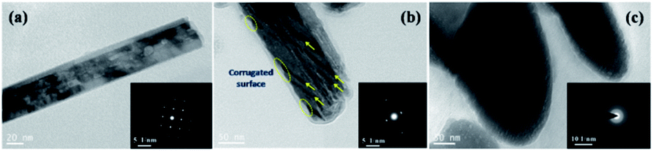 | ||
| Fig. 4 TEM images and corresponding SAED patterns of (a) pristine and irradiated samples with (b) 5 × 10¹² and (c) 5 × 10¹³ ions per cm2 fluences. The arrows and yellow ellipses in (b) respectively indicate the ion tracks and the corrugated surface as a result of 100 MeV Ag ion irradiation (at a fluence of 5 × 10¹² ions per cm2). | ||
Chemical compositions of pristine and irradiated nanorods were investigated by XPS. Fig. 5 presents (a) Ti 2p and (b) O 1s spectra of pristine and irradiated (5 × 10¹² and 5 × 10¹³ ions per cm2) samples. The peaks located at 457.47 eV and 463.06 eV (in Fig. 5(a)) are attributed to Ti 2p3/2 and Ti 2p1/2, respectively, and correspond to the Ti4+ state.49Fig. 5(a) shows no significant change in the peak position and shape after Ag ion irradiation. However, the peak intensities decrease compared to that of pristine nanorods, which indicates a reduction in Ti4+ content in the sample.50 The O 1s peak in Fig. 5(c) shows three components attributed to the lattice oxygen of TiO2 (528.06 eV), oxygen vacancies (529.67 eV), and surface adsorbed oxygen (530.58 eV).51Fig. 5(b) shows that the contribution from oxygen vacancies becomes stronger in irradiated samples. After irradiation at fluences of 5 × 10¹² ions per cm2 and 5 × 10¹³ ions per cm2, the peaks shift to the higher binding energies observed from Fig. 5(d) and (e). The peak positions in terms of binding energies (in eV) of Ti and O are presented in Table 1. The observed shift is attributed to the irradiation-induced changes in the electronic structure, as also observed in the case of ZnO nanorods.52
 | ||
| Fig. 5 XPS spectra (a) Ti 2p spectra and (b) O 1s spectra of pristine and irradiated samples at fluences of 5 × 10¹² and 5 × 10¹³ ions per cm2, (c), (d) and (e) present the fitted O 1s spectra of individuals. | ||
| Chemical state of elements | Pristine | 5 × 10¹² ions per cm2 | 5 × 10¹³ ions per cm2 |
|---|---|---|---|
| Ti 2p3/2 | 457.47 | 457.34 | 457.34 |
| Ti 2p1/2 | 463.06 | 463.06 | 463.06 |
| O 1s (lattice oxygen) | 528.06 | 528.40 | 528.54 |
| O 1s (oxygen vacancy) | 529.67 | 529.96 | 530.27 |
| O 1s (adsorbed oxygen) | 530.58 | 531.05 | 531.33 |
3.2. Thermal spike calculation
It is important to quantify the energy deposited by an irradiating ion to estimate the heat dissipation and thermal spike-induced effects in the material. To have a detailed analysis of the ion–matter interaction, the electronic and atomic (lattice) temperature evolution profiles were simulated in the framework of the inelastic thermal spike (i-TS) model.53 The i-TS model considers the target material comprising two components, namely, electronic and atomic subsystems. The transient heat diffusion process between the incident ion and the two subsystems is well described by a set of coupled differential equations in a cylindrical geometry (r, z, t), which are as follows:53 | (1) |
 | (2) |
Fig. 6(a) shows that the electronic subsystem retains the energy deposited by the incident ion for a very short period (∼10−15 s) and then it is transferred to the lattice subsystem via electron–phonon coupling controlled by the parameter g. It is observed from Fig. 6(b) that the lattice temperature reaches the melting point of TiO2 (2130 K)27 at 5.5 × 10⁻¹⁵ s and the boiling point (3200 K)27 at 2.3 × 10⁻¹⁴ s. Fig. 6(b) also shows that the temperature within a radius of 5.5 nm exceeds the melting point of 2130 K. This observation is in agreement with the lateral dimension (∼10 nm) of the track as observed from high-resolution TEM images (Fig. 4(b)). According to the thermal spike model, the ion track appears as a consequence of the re-solidification during the rapid quenching of the molten state along the ion trajectory. Fig. 6(b) shows that the quenching from the molten state starts at 5.2 × 10⁻¹¹ s, enabling us to ascribe the SHI-induced track formation to the rapid quenching of the thermal spike. Further, melting of the material as predicted by the i-TS model explains the observations in the SEM images (Fig. 1), which show a thin layer of material connecting the adjacent nanorods.
 | ||
| Fig. 6 (a) Electronic and (b) lattice temperature profiles along the radial distance from the center of the ion trajectory with the evolution of time. | ||
The interaction of the 100 MeV Ag ion beam with TiO2 nanorod arrays is schematically shown in Fig. 7. At a relatively lower fluence (5 × 10¹² ions per cm2), tracks are formed inside the material preserving the tetragonal shape of each nanorod. However, at the highest fluence (5 × 10¹³ ions per cm2), individual ion tracks overlap that result in the overall melting of the nanorods. Being in a molten state, the nanorods start to bend and interconnect with adjacent nanorods through the diffusion of molten layers. Due to the rapid quenching of the molten state, significant distortions of the crystalline structure and the tetragonal shape occur along with the appearance of interconnected nanostructure morphology. Initially, TRIM simulation42 (Fig. S3(c)†) was performed to quantify the disorder created inside the TiO2 lattice. However, the TRIM code42 does not account for the thermal spike phenomenon and therefore provides an under-estimation of the disorder compared to the experimental observations. In the present study, the disorderliness is highly pronounced as a consequence of thermal spike and rapid quenching.
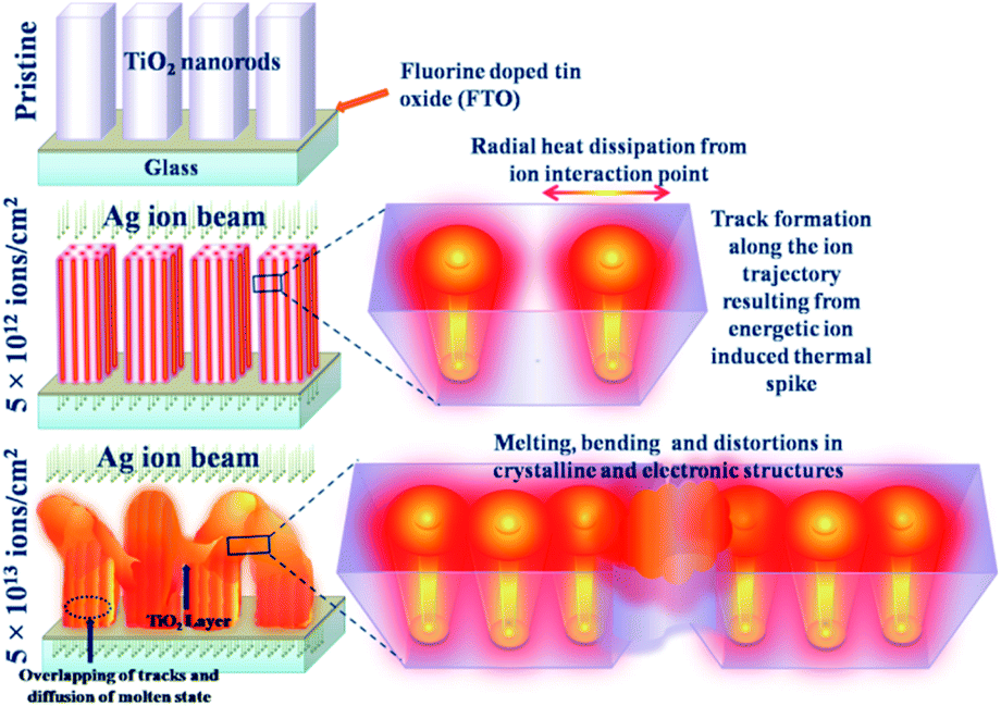 | ||
| Fig. 7 Schematic presentation of the effect of high energy ion irradiation on the TiO2 nanorods at different fluences (5 × 10¹² ions per cm2 and 5 × 10¹³ ions per cm2). | ||
3.3. Optical property study
The optical absorption of the pristine and irradiated TiO2 nanorod arrays was characterized by diffuse reflectance spectroscopy. Fig. 8(a) and (b) show the diffuse reflectance and absorbance spectra of the pristine and irradiated samples with fluences of 5 × 10¹² and 5 × 10¹³ ions per cm2. To estimate the effective bandgap, the Kubelka–Munk function55 was used to obtain the Tauc plot, as shown in Fig. 8(c). It is observed that the reflectance from the irradiated samples in the visible region is systematically reduced compared to that of pristine TiO2 nanorod arrays. This suggests an enhancement in the visible light absorption that can be attributed to enhanced disorder caused by irradiation, which in turn leads to a higher surface area. Fig. 8(c) shows bandgap values obtained by the slope method, which are 3.11 eV for pristine and 3.23 eV for the sample irradiated at a fluence of 5 × 10¹² ions per cm2. On the other hand, the sample irradiated at 5 × 10¹³ ions per cm2 shows an indirect bandgap of 3.10 eV (Fig. 8(d)). The position of the band edge at 3.11 eV for the pristine sample matches with the bandgap of rutile TiO2.8 It is reported that irradiation-induced lattice distortion is mainly caused by oxygen vacancies.30 The presence of the oxygen vacancies induces microstrain, as also observed from the XRD peak shift (Fig. 2). For the irradiation at a fluence of 5 × 10¹² ions per cm2, ion tracks lead to a structural distortion in the TiO2 matrix. The reported optical bandgap value of the amorphous TiO2 is 3.38 eV,30 which is higher than that of rutile TiO2. Therefore, the higher band edge position (compared to that of pristine) at 3.23 eV indicates a significant structural distortion in the irradiated samples. However, for the highest fluence (5 × 10¹³ ions per cm2), an indirect bandgap appears. The direct to indirect transition in the bandgap is also observed from the DFT-based analysis discussed in the subsequent section.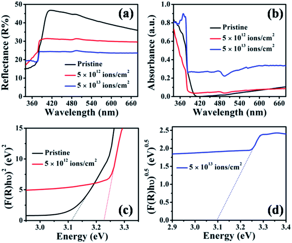 | ||
| Fig. 8 (a) UV-Vis diffuse reflectance spectra, (b) absorbance spectra and (c and d) Tauc plots of pristine and samples irradiated at 5 × 10¹² and 5 × 10¹³ ions per cm2 fluences. | ||
The luminescence characteristics of the pristine and irradiated nanorods were investigated by PL spectroscopy, and the spectra are presented in Fig. 9. The PL spectrum of the pristine sample exhibits a prominent peak at 408 nm attributed to the near-band-gap emission and a peak at 467 nm, a characteristic peak for the rutile TiO2.56 Other small peaks at 450 nm, 482 nm, and 492 nm may arise from low-intensity radiative transitions between sub-band-gap states. The PL peaks do not show any significant shift after ion irradiation, but a decrease in intensities is observed. The peak at 408 nm is significantly reduced in intensity for the irradiated samples due to the incorporation of lattice defects and disorder build-up with increasing ion fluence. However, the peak at 467 nm suggests that some extent of the rutile structure persists even after the irradiation at the highest fluence of 5 × 10¹³ ions per cm2.
 | ||
| Fig. 9 PL spectra of pristine and irradiated samples with 1 × 10¹², 5 × 10¹², 1 × 10¹³ and 5 × 10¹³ ions per cm2 fluences. 320 nm wavelength was used for excitation. | ||
3.4. Electronic structure using the DFT study
Insight into the transition from the direct to the indirect bandgap with irradiation-induced deformed structures can be obtained from the DFT calculations. The DFT methods for the periodic systems can be implemented because, despite deformation, periodicity remains in a larger domain as revealed by distinct XRD peaks. DFT studies on such systems can explain the effect of local distortion on the electronic structure.The calculations have been performed using the plane-wave-pseudopotential approach as implemented in Quantum ESPRESSO.57 The experimentally obtained lattice parameters of the tetragonal structure of the rutile TiO2 estimated by Rietveld refinement of XRD data have been considered for the calculations. The Vanderbilt ultrasoft pseudopotentials are used to describe the electron–ion interactions,58 in which the valence states of Ti include 12 electrons from 3s, 3p, 4s and 3d, and that of O includes 6 electrons from 2s and 2p shells. The exchange-correlation functional is approximated through the PBE-GGA functional.59 The convergence criterion for self-consistent energy is taken to be 10−8 Ry. A k-mesh of 8 × 8 × 8 is used for the Brillouin zone integration. The kinetic energy cut-off for the electron wave functions is set at 30 Ry, and the augmented charge density cut-off is set to be 300 Ry. Our previous analysis on TiO2 tells that with these sets of parameters, the lattice parameters for the case of anatase TiO2 match with that of the theoretical and experimental reports.60,61
The rutile TiO2 crystallizes in a tetragonal structure with P42/mnm (space group #136). Each unit cell contains two formula units of TiO2, in which each Ti atom is coordinated with six O atoms and each O atom to three Ti atoms, as shown in Fig. 10(a). The TiO2 octahedra are slightly distorted and connected at the edge through O atoms. In the present work, we have used the experimental lattice parameters obtained from the XRD data. For pristine TiO2, the observed lattice parameters are a = 4.575 Å and c = 2.936 Å. When the structure is subjected to a fluence of 5 × 10¹² ions per cm2, the Ti–O bond undergoes slight distortion (Fig. 10(b)), indicating a structural transformation from the crystalline to the quasidisordered state. At a fluence of 5 × 10¹³ ions per cm2, the structure undergoes a larger distortion which is clear from the breakdown of TiO6 octahedra as presented in Fig. 10(c). Although the lattice parameter is hardly affected, the distortion of the Ti–O bond is quite significant, and its impact on the band structure is discussed in the following section.
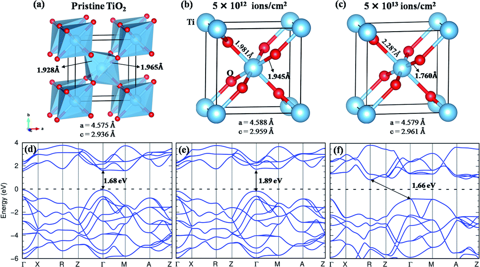 | ||
| Fig. 10 (a) The structure of pristine rutile TiO2 showing the corner-sharing TiO6 octahedra. (b and c) The structure of TiO2 when subjected to fluences of 5 × 10¹² and 5 × 10¹³ ions per cm2, respectively. It shows the change in the bond length of TiO6 octahedra in the latter case. (d) The band structure of pristine rutile TiO2 showing a direct bandgap of 1.68 eV with GGA calculation. (e and f) The band structure corresponding to (b) and (c) respectively. The Fermi level is set to be at zero. The Ti and O atoms are represented by light blue and red solid spheres, respectively. | ||
With the GGA exchange-correlation functional, a direct bandgap is observed for pristine TiO2 having a value of 1.68 eV with the band minima at the high symmetry point Γ (Fig. 10(d)). It is well understood that the GGA functional underestimates the bandgap.62 Although the GGA + U can approximate the bandgap to the experimental value;63 however, in the present situation, the GGA functional is sufficient to provide a comparison of the change in the bandgap with the structural deformation. At a fluence of 5 × 10¹² ions per cm2, a minor structural distortion takes place as a result of which the band dispersive nature remains almost like that of the pristine structure except for an increase in the bandgap by 0.21 eV (Fig. 10(e)). When the structure is subjected to a fluence of 5 × 10¹³ ions per cm2, the band dispersion changes due to distortion of the Ti–O bond (Fig. 10(f)). It goes from the direct bandgap to the indirect bandgap system, where the valence band maxima are observed at Γ and M points and the conduction band minimum is at the R point. The intertwined Ti-d – O-p – Ti-d covalent interactions play a major role in the band dispersion of the lower-lying conduction bands. The increase in bond length and further tilting of the Ti–O–Ti axis modify this interaction to create the CBM at R instead of Γ. Such a direct to indirect transition of the bandgap has also been observed in ZnO and Si nanowires.64–66
4. Conclusions
We have reported the effect of 100 MeV Ag ion beam irradiation on vertically oriented TiO2 nanorods grown on an FTO coated glass substrate. The nanorods undergo a significant morphological and structural transformation through bending and melting induced by a localized thermal spike, particularly at the highest fluence (5 × 10¹³ ions per cm2). High-resolution TEM analysis shows tracks with a lateral dimension of ∼10 nm along the ion trajectory. Thermal spike simulation confirms the melting in TiO2 nanorods within a cylindrical region having a radius of ∼5.5 nm, supporting the TEM observation. Re-solidification during the rapid quenching of the SHI-induced thermal spike within a time interval of ∼0.5 picoseconds is responsible for the deformation of the crystalline structure, as also observed in the XRD and Raman data. XPS analysis reveals the presence of ion beam-induced vacancies in the lattice, and the resulting strain is manifested by the shift in XRD and Raman peaks. An interesting feature of the irradiation is the transition from a direct to an indirect bandgap at the highest fluence (5 × 10¹³ ions per cm2), which is also supported by the electronic band structure calculation using DFT. Hence, the localized modification of the TiO2 nanorods induced by high energy ion beam irradiation offers unique features in terms of crystallinity, morphology and electronic band structure.Conflicts of interest
There are no conflicts to declare.Acknowledgements
The authors are thankful to M. S. R. Rao, professor of Department of Physics, IIT Madras for X-ray diffractometer, the NFMTC/MSRC/IITM facility under the project No. SR/NM/NAT-02/2005 & DST/NM/JIIT-01/2016. The authors are also grateful to T. Pradeep, professor of Department of Chemistry, and the Department of Science and Technology (DST) unit of Nanoscience, IIT Madras, for XPS facilities. S. Dey would like to thank M. P. Kannan for the assistance in analyzing the XPS data Dhruba Das for XRD characterization and Swati Dhua for asistance in experiments. The authors also acknowledge the Sophisticated Analytical Instrument Facility (SAIF), IIT Madras for UV-Vis and PL spectroscopy facilities. The authors also would like to thank the Department of Physics, IIT Madras, for providing the research-related facilities and funding. The authors are also grateful to IUAC, New Delhi, for the ion beam facility.References
- M. K. Nowotny, L. R. Sheppard, T. Bak and J. Nowotny, J. Phys. Chem. C, 2008, 112, 5275–5300 CrossRef CAS.
- S. Wang, L. Pan, J. J. Song, W. Mi, J. J. Zou, L. Wang and X. Zhang, J. Am. Chem. Soc., 2015, 137, 2975–2983 CrossRef CAS PubMed.
- D. Kanjilal, Curr. Sci., 2001, 80, 1560–1566 CAS.
- C. Notthoff, S. Jordan, A. Hadley, P. Mota-Santiago, R. G. Elliman, W. Lei, N. Kirby and P. Kluth, Phys. Rev. Mater., 2020, 4, 046001 CrossRef CAS.
- N. A. Nebogatikova, I. V. Antonova, S. V. Erohin, D. G. Kvashnin, A. Olejniczak, V. A. Volodin, A. V. Skuratov, A. V. Krasheninnikov, P. B. Sorokin and L. A. Chernozatonskii, Nanoscale, 2018, 10, 14499–14509 RSC.
- L. Madauß, I. Zegkinoglou, H. Vázquez Muiños, Y. W. Choi, S. Kunze, M. Q. Zhao, C. H. Naylor, P. Ernst, E. Pollmann, O. Ochedowski, H. Lebius, A. Benyagoub, B. Ban-D'Etat, A. T. C. Johnson, F. Djurabekova, B. Roldan Cuenya and M. Schleberger, Nanoscale, 2018, 10, 22908–22916 RSC.
- M. Toulemonde, C. Trautmann, E. Balanzat, K. Hjort and A. Weidinger, Nucl. Instrum. Methods Phys. Res., Sect. B, 2004, 216, 1–8 CrossRef CAS.
- P. Roy, S. Berger and P. Schmuki, Angew. Chem., Int. Ed., 2011, 50, 2904–2939 CrossRef CAS PubMed.
- N. Khatun, S. Tiwari, C. P. Vinod, C. M. Tseng, S. Wei Liu, S. Biring and S. Sen, J. Appl. Phys., 2018, 123, 245702 CrossRef.
- M. Thakurdesai, D. Kanjilal and V. Bhattacharyya, Appl. Surf. Sci., 2008, 254, 4695–4700 CrossRef CAS.
- M. Thakurdesai, T. Mohanty, D. Kanjilal, P. Raychaudhuri and V. Bhattacharyya, Appl. Surf. Sci., 2009, 255, 8935–8940 CrossRef CAS.
- M. Thakurdesai, D. Kanjilal and V. Bhattacharyya, Semicond. Sci. Technol., 2009, 24, 085023 CrossRef.
- R. Hazem, M. Izerrouken, A. Sari, S. Kermadi, M. Msimanga, A. Benyagoub, M. Maaza, M. Belgaid and M. Boumaour, Nucl. Instrum. Methods Phys. Res., Sect. B, 2013, 304, 16–22 CrossRef CAS.
- H. Rath, P. Dash, T. Som, P. V. Satyam, U. P. Singh, P. K. Kulriya, D. Kanjilal, D. K. Avasthi and N. C. Mishra, J. Appl. Phys., 2009, 105, 074311 CrossRef.
- S. Gautam, K. H. Chae, H. Thakur, R. Kumar, P. Thakur, N. B. Brookes and K. K. Sharma, J. Appl. Phys., 2011, 110, 083718 CrossRef.
- S. K. Gautam, A. Chettah, R. G. Singh, S. Ojha and F. Singh, Nucl. Instrum. Methods Phys. Res., Sect. B, 2016, 379, 224–229 CrossRef CAS.
- M. Thakurdesai, A. Mahadkar, D. Kanjilal and V. Bhattacharyya, Vacuum, 2008, 82, 639–644 CrossRef CAS.
- R. Sanz, J. Jensen, A. Johansson, M. Skupinski, G. Possnert, M. Boman, M. Hernandez-Vélez, M. Vazquez and K. Hjort, Nanotechnology, 2007, 18, 305303 CrossRef.
- K. ichi Nomura, T. Nakanishi, Y. Nagasawa, Y. Ohki, K. Awazu, M. Fujimaki, N. Kobayashi, S. Ishii and K. Shima, Phys. Rev. B: Condens. Matter Mater. Phys., 2003, 68, 064106 CrossRef.
- J. Jensen, M. Skupiński, K. Hjort and R. Sanz, Nucl. Instrum. Methods Phys. Res., Sect. B, 2008, 266, 3113–3119 CrossRef CAS.
- K. Awazu, M. Fujimaki, Y. Ohki and T. Komatsubara, Radiat. Meas., 2005, 40, 722–729 CrossRef CAS.
- M. Karlušić, M. Jakšić, H. Lebius, B. Ban-D'Etat, R. A. Wilhelm, R. Heller and M. Schleberger, J. Phys. D: Appl. Phys., 2017, 50, 205302 CrossRef.
- M. Karlušic, S. Bernstorff, Z. Siketic, B. Šantic, I. Bogdanovic-Radovic, M. Jakšic, M. Schleberger and M. Buljan, J. Appl. Crystallogr., 2016, 49, 1704–1712 CrossRef.
- J. H. O'Connell, V. A. Skuratov, A. Akilbekov, A. Zhumazhanova and A. Janse Van Vuuren, Nucl. Instrum. Methods Phys. Res., Sect. B, 2016, 379, 200–205 CrossRef.
- J. O'Connell, V. Skuratov, A. J. van Vuuren, M. Saifulin and A. Akilbekov, Phys. Status Solidi B, 2016, 253, 2144–2149 CrossRef.
- J. H. O'Connell, G. Aralbayeva, V. A. Skuratov, M. Saifulin, A. Janse Van Vuuren, A. Akilbekov and M. Zdorovets, Mater. Res. Express, 2018, 5, 055015 CrossRef.
- K. Awazu, X. Wang, M. Fujimaki, T. Komatsubara, T. Ikeda and Y. Ohki, J. Appl. Phys., 2006, 100, 044308 CrossRef.
- P. Zhai, S. Nan, L. Xu, W. Li, Z. Li, P. Hu, J. Zeng, S. Zhang, Y. Sun and J. Liu, Nucl. Instrum. Methods Phys. Res., Sect. B, 2019, 457, 72–79 CrossRef CAS.
- S. K. Gautam, F. Singh, I. Sulania, R. G. Singh, P. K. Kulriya and E. Pippel, J. Appl. Phys., 2014, 115, 143504 CrossRef.
- H. Rath, P. Dash, U. P. Singh, D. K. Avasthi, D. Kanjilal and N. C. Mishra, Nucl. Instrum. Methods Phys. Res., Sect. B, 2015, 365, 553–559 CrossRef CAS.
- J. Deng, Y. Su, D. Liu, P. Yang, B. Liu and C. Liu, Chem. Rev., 2019, 119, 9221–9259 CrossRef CAS.
- M. Wang, J. Duan, J. Du, X. Yang, Y. Duan, T. Zhang and Q. Tang, ACS Appl. Mater. Interfaces, 2021, 13, 12091–12098 CrossRef CAS.
- J. W. Yoon, D. H. Kim, J. H. Kim, H. W. Jang and J. H. Lee, Appl. Catal., B, 2019, 244, 511–518 CrossRef CAS.
- J. I. Jang, Y. H. Shin, Y. S. Kim, A. D. Nguyen, T. H. Pham, T. K. Nguyen, H. Ullah, Z. Tahir, Y. C. Park and J. Park, ACS Appl. Energy Mater., 2020, 3, 10854–10862 CrossRef.
- D. Wang, L. Chen, Z. Ding and X. Feng, Sol. RRL, 2019, 4, 1900185 CrossRef.
- Y. Gao, J. Xu, S. Shi, H. Dong, Y. Cheng, C. Wei, X. Zhang, S. Yin and L. Li, ACS Appl. Mater. Interfaces, 2018, 10, 11269–11279 CrossRef CAS PubMed.
- H. K. Ramamurthy Rao, E. Gemechu, U. Thakur, K. Shankar and A. Kumar, Sol. Energy Mater. Sol. Cells, 2021, 230, 111288 CrossRef CAS.
- X. Feng, K. Shankar, O. K. Varghese, M. Paulose, T. J. Latempa and C. A. Grimes, Nano Lett., 2008, 8, 3781–3786 CrossRef CAS.
- M. Zu, M. Zheng, S. Zhang, C. Xing, M. Zhou, H. Liu, X. Zhou and S. Zhang, Sens. Actuators, B, 2020, 321, 128504 CrossRef CAS.
- S. Dey and S. C. Roy, Nano Express, 2021, 2, 010028 CrossRef.
- D. Kanjilal, S. Chopra, M. M. Narayanan, I. S. Iyer, V. Jha, R. Joshi and S. K. Datta, Nucl. Instrum. Methods Phys. Res., Sect. A, 1993, 328, 97–100 CrossRef.
- J. F. Ziegler, M. D. Ziegler and J. P. Biersack, Nucl. Instrum. Methods Phys. Res., Sect. B, 2010, 268, 1818–1823 CrossRef CAS.
- S. Dey and S. C. Roy, J. Alloys Compd., 2021, 881, 160481 CrossRef CAS.
- M. Li, X. Zhang, Y. Liu and Y. Yang, Appl. Surf. Sci., 2018, 440, 1172–1180 CrossRef CAS.
- Y. Zhang, C. X. Harris, P. Wallenmeyer, J. Murowchick and X. Chen, J. Phys. Chem. C, 2013, 117, 24015–24022 CrossRef CAS.
- H. Rath, B. N. Dash, A. Benyagoub and N. C. Mishra, Sci. Rep., 2018, 8, 11774 CrossRef.
- R. Hazem, M. Izerrouken, A. Cheraitia and A. Djehlane, Nucl. Instrum. Methods Phys. Res., Sect. B, 2019, 444, 62–67 CrossRef CAS.
- H.-H. Chou, S. Y.-H. Liou and M. Calatayud, Catal. Today, 2020, 356, 49–55 CrossRef CAS.
- B. Bharti, S. Kumar, H. N. Lee and R. Kumar, Sci. Rep., 2016, 6, 32355 CrossRef CAS PubMed.
- A. Manna, A. Barman, S. R. Joshi, B. Satpati, P. Dash, A. Chattaraj, S. K. Srivastava, P. K. Sahoo, A. Kanjilal, D. Kanjilal and S. Varma, J. Appl. Phys., 2018, 124, 155303 CrossRef.
- J. Li, H. Zhou, H. Zhuo, Z. Wei, G. Zhuang, X. Zhong, S. Deng, X. Li and J. Wang, J. Mater. Chem. A, 2018, 6, 2264–2272 RSC.
- K. S. Ranjith, L. R. Nivedita, K. Asokan, S. Krishnamurthy, R. Pandian, M. Kamruddin, D. K. Avasthi and R. T. Rajendra Kumar, Sci. Rep., 2017, 7, 3251 CrossRef PubMed.
- C. Dufour, V. Khomenkov, G. Rizza and M. Toulemonde, J. Phys. D: Appl. Phys., 2012, 45, 065302 CrossRef.
- S. Monticone, R. Tufeu, A. V. Kanaev, E. Scolan and C. Sanchez, Appl. Surf. Sci., 2000, 162, 565–570 CrossRef.
- S. Dey and S. C. Roy, Ceram. Int., 2021, 47, 14603–14611 CrossRef CAS.
- M. Maria Angelin Sinthiya, N. Kumaresan, K. Ramamurthi, K. Sethuraman, S. Moorthy Babu, R. Ramesh Babu and V. Ganesh, Appl. Surf. Sci., 2018, 449, 122–131 CrossRef.
- P. Giannozzi, J. Phys. Condens. Matter, 2017, 29, 465901 CrossRef CAS PubMed.
- D. Vanderbilt, Phys. Rev. B: Condens. Matter Mater. Phys., 1990, 41, 7892–7895 CrossRef.
- J. P. Perdew, K. Burke and M. Ernzerhof, Phys. Rev. Lett., 1996, 77, 3865–3868 CrossRef CAS.
- S. B. Mishra, A. Choudhary, S. C. Roy and B. R. K. Nanda, Phys. Rev. Mater., 2018, 2, 115801 CrossRef CAS.
- S. B. Mishra and B. R. K. Nanda, Appl. Surf. Sci., 2020, 531, 147330 CrossRef CAS.
- S. Di Mo and W. Y. Ching, Phys. Rev. B: Condens. Matter Mater. Phys., 1995, 51, 13023–13032 CrossRef.
- S. B. Mishra, S. C. Roy and B. R. K. Nanda, Appl. Surf. Sci., 2021, 542, 148709 CrossRef CAS.
- S. Li, J. L. Li, Q. Jiang and G. W. Yang, J. Appl. Phys., 2010, 108, 024302 CrossRef.
- L. Shi and G. Zhang, J. Electron. Mater., 2016, 45, 5391–5394 CrossRef CAS.
- I. J. T. Jensen, A. G. Ulyashin and O. M. Løvvik, J. Appl. Phys., 2016, 119, 015702 CrossRef.
Footnote |
| † Electronic supplementary information (ESI) available. See DOI: 10.1039/d1na00666e |
| This journal is © The Royal Society of Chemistry 2022 |