
 Open Access Article
 This Open Access Article is licensed under a Creative Commons Attribution-Non Commercial 3.0 Unported Licence
A merged lattice metal nanohole array based dual-mode plasmonic laser with an ultra-low threshold
Shadman
Shahid†
 ,
Shahed-E-
Zumrat†
and
Muhammad Anisuzzaman
Talukder
*
,
Shahed-E-
Zumrat†
and
Muhammad Anisuzzaman
Talukder
*
Department of Electrical and Electronic Engineering, Bangladesh University of Engineering and Technology, Dhaka 1205, Bangladesh. E-mail: anis@eee.buet.ac.bd
First published on 10th December 2021
Abstract
Plasmonic lasers offer great potential for cutting-edge, disruptive applications. However, they suffer from a high loss in metals, lack of spatial coherence in the near field, and divergent far-field emission. The challenges are even more significant for a plasmonic laser emitting more than one wavelength mode. The design complexity required for creating multiple modes often limits avenues for minimizing losses and converging far-field emission patterns. This work exploits plasmonic resonances at the junction of a merged lattice metal nanohole array (NHA) and a one-dimensional photonic crystal to achieve dual-mode lasing. The merged lattice NHA is designed by concentrically combining two simple NHAs with different periodicities to create pseudo randomness, leading to enhanced localization and confinement of light in multiple wavelength modes. The proposed structure notably produces intense dual-mode lasing at an ultra-low threshold compared to recent state-of-the-art plasmonic laser demonstrations. The wavelengths of the lasing modes and the separation between them can be tuned over a broad range by changing the structural parameters. The proposed laser also creates a highly directional far-field pattern with a divergence angle of only <0.35°.
1 Introduction
Coherent light sources with sub-wavelength dimensions have fundamental applications and applied significance. The dimensional barriers in laser designs are often overcome by employing the concept of plasmonics, confining light within a sub-wavelength dimension by exciting surface plasmon modes. Miniaturized plasmonic lasers are potential candidates for applications in sensing and spectroscopy, efficient on-chip optical interconnects, nanolithography, super-resolution imaging, biomedical imaging, interconnection between optical and microelectronic devices, and detection of nanoscale biomolecules.1–14 Coherent amplification of surface plasmons in a plasmonic laser, first proposed in 2003,15 emulates the coherent stimulated emission of photons in conventional lasers. Since then, we have witnessed a plethora of research activities on various topologies to design efficient, low threshold, and highly directional plasmonic lasers.16–22 Plasmonic lasers are usually composed of an isolated nanostructure or a periodic array of nanostructures. With the advancement of nanophotonics, the demand for coherent light sources at the nanoscale dimension has increased drastically. Therefore, ample research opportunities lie in the design of such light sources to meet specific needs.Lasers that emit multiple distinct wavelength modes are essential for various applications, including sensing multiple target substances simultaneously, distance measurements using two-wavelength interferometry, terahertz difference frequency generation, frequency mixing, frequency division multiplexing, and wavelength division multiplexing in optical circuits.23–32 To date, multimode solid-state and semiconductor lasers have been significantly explored.33–35 Nonetheless, it is a great challenge to operate these devices at room temperature due to the temperature-sensitive gain of semiconductor lasers. The increase in the non-radiative recombination rate at room temperature severely reduces the optical gain of semiconductor lasers. By contrast, research on multimode plasmonic lasers has attracted attention only recently. The first multimode plasmonic laser, reported by Wang et al. in 2017, exploited multiple band-edge modes excited using a plasmonic superlattice.36 The designed plasmonic superlattice consisted of periodic nanoparticles on periodic patches to obtain dual-mode lasing. Wang et al. obtained an emission linewidth of <0.5 nm, a mode separation of ∼10 nm, and a divergence angle of <1° from a centimeter-squared device area.
Recently, Pourjamal et al. obtained dual-mode lasing by breaking the symmetry of a two-dimensional (2D) ferromagnetic nickel plasmonic nanodisk array using different periodicities along the x- and y-directions.37 However, different periodicities along the axes result in a destructive spatial interference in the far field, thus increasing the divergence angle and making the emission less coherent in the spatial domain than if periodicities along the axes are equal. Pourjamal et al. demonstrated dual-mode lasing in the visible wavelength range with an emission linewidth of <1 nm, a mode separation of ∼15 nm, and a divergence angle of ∼5.7°. More recently, Winkler et al. utilized a plasmonic nanoparticle lattice embedded in a viscous quantum-dot film to exhibit dual-wavelength lasing.38 They adopted two methods to produce dual-mode lasing: firstly, using a rectangular silver (Ag) nanoparticle lattice; and secondly, using a thin quantum-dot film.38 They obtained an emission linewidth of ∼1 nm, a mode separation of ∼19 nm, and a divergence angle of 11.74° and 5.6° along the x- and y-directions. These approaches for plasmonic dual-mode lasing either result in a bulky laser structure due to the two-fold symmetry36 or create a divergent far-field pattern due to different periodicities in the x- and y-directions.37,38 Furthermore, breaking the symmetry of the structure in the two in-plane directions incurs additional losses by generating off-normal spatial lasing modes. These structures have also proved to be inherently lossy, thus requiring a high threshold of pump energy.
This work proposes an alternative technique for dual-mode emission from a plasmonic laser. The proposed plasmonic laser comprises an organic gain medium with a distributed Bragg reflector (DBR) as a one-dimensional (1D) photonic crystal (PhC) on one side and a merged lattice metal nanohole array (NHA) on the other side. While the merged lattice configuration helps us achieve a directional dual-mode lasing, the DBR lets us control the emission directionality and the relative intensity of the lasing modes. The basic principle is to intelligently utilize states formed by holes perforated in the metal film to create the optical feedback necessary to support dual-mode emission. The DBR acts as a filter to separate the input pump frequency of the gain medium from lasing emission frequencies. Additionally, the optical Tamm state plasmons, also known as Tamm plasmons (TPs), excited at the interface between the DBR and metal NHA and the structural pseudo-randomness-mediated strong light confinement within the laser cavity contribute to enhanced lasing emission. The dual-mode lasing emissions are highly directional as the proposed structure creates only the zeroth-order mode by employing sub-wavelength hole dimensions and periodicity in the metal NHA.
The proposed merged lattice metal NHA plasmonic laser produces dual-mode lasing in the near-infrared region. The required threshold pump energy is at least two orders of magnitude smaller than that required by several state-of-the-art demonstrations. The lasing modes have a divergence angle of ≲0.35°, and a narrow linewidth of ∼3 nm for the smaller wavelength mode and ∼1.5 nm for the longer wavelength mode. The emission wavelengths can be tuned over a broad range of ∼845–883 nm for the smaller wavelength lasing mode and ∼860–886 nm for the longer wavelength lasing mode, and the mode separation becomes as much as ∼15 nm by changing the structural parameters.
We organize the rest of the paper as follows: Sec. 2 presents the proposed dual-mode plasmonic laser, including a discussion on the design principles of the merged lattice metal NHA structure that produces dual-mode emission. Section 3 describes the simulation methodology used to calculate the interactions between the incident pump pulse and the laser structure, and the lasing dynamics of the proposed laser. In Sec. 4, we present and discuss results, including the transmission spectra of the merged lattice gold (Au) NHA and passive optical cavity; and the near- and far-field emission profiles. Finally, in Sec. 5, we conclude on the findings.
2 Proposed merged lattice plasmonic laser structure
The proposed merged lattice plasmonic laser structure is shown in Fig. 1. At the core of the proposed plasmonic laser's optical cavity, the gain medium consists of IR-140 dye molecules embedded in a polyurethane (PU) matrix. The parameters of this gain medium are tabulated in Table 1. The dye molecules absorb the incident pump energy and offer gain to the radiative lasing emission. On one side of the gain medium, opposite to the optical pump, a 100 nm-thick Au film is perforated with nanoholes. On the other side, there is a 1D PhC consisting of alternating layers of TiO2 and MgF2. Unless stated otherwise, we assume that the proposed laser contains five pairs of TiO2–MgF2 layers.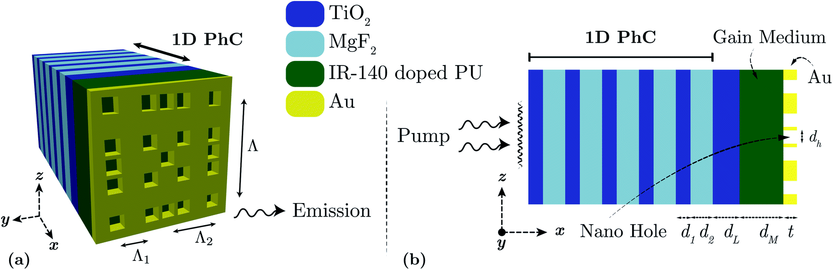 | ||
| Fig. 1 (a) The 3D schematic diagram of the proposed laser. All components have been drawn to actual scale. (b) Schematic diagram of a longitudinal section across the structure. TiO2 layer thickness d1 = 109 nm, MgF2 layer thickness d2 = 165 nm, terminating TiO2 layer thickness dL = 200 nm, gain medium thickness dM = 325 nm, and Au NHA thickness t = 100 nm. In the merged lattice NHA structure, the two short-scale periods are Λ1 = 250 nm, Λ2 = 375 nm. The primitive unit cell has a period of Λ = 750 nm. The square hole width is dh = 100 nm for all the nanoholes. | ||
| Parameter | Value |
|---|---|
| Absorption wavelength (λ03) | 800 nm |
| Emission wavelength (λ21) | 870 nm |
| Index of the PU material | 1.51 |
| Dye concentration | 2 × 1018 cm−3 |
![[thin space (1/6-em)]](https://www.rsc.org/images/entities/char_2009.gif) |
|
| Transition lifetimes | |
| τ 30 = τ21 | 1 ns |
| τ 32 = τ10 | 10 fs |
In the metal layer, square hole arrays with two different periodicities are superposed, as shown in Fig. 2. The square holes have dimensions of 100 nm × 100 nm on the yz-plane. In the densely placed square hole array, the hole periodicity (Λ1) is 250 nm, as shown in Fig. 2(a). On the other hand, in the sparsely placed square hole array, the hole periodicity (Λ2) is 375 nm, as shown in Fig. 2(b). In both NHAs, four corners have identical square holes in the same places. These two short-scale periodicities maintain a fixed ratio of r = Λ2/Λ1 = 3/2. The value of r is constrained by r = R/(R − 1), where R is the least integer multiple of r.39 Here, we choose R = 3 in the designed merged lattice NHA. In our proposed structure, the two square hole arrays with periodicities Λ1 and Λ2 are superposed keeping them concentric so that the merged lattice becomes a square lattice with a primitive unit cell periodicity of Λ = RΛ1 in both the y- and z-directions, as shown in Fig. 2(c). The holes at the four corners of the merged lattice overlap from both the densely and sparsely placed NHAs.
 | ||
| Fig. 2 (a) R unit cells of a simple NHA with a square lattice of period Λ1 = 250 nm, and (b) R − 1 unit cells of a simple NHA with a square lattice of period Λ2 = 375 nm. (c) One primitive unit cell of the merged lattice NHA with period Λ = 750 nm. | ||
3 Simulation methodology
We have carried out time- and frequency-domain investigations to study the proposed structure's lasing performance and characterize its electromagnetic response. To compute the electromagnetic dynamics involved in the lasing action and obtain the required data, we have solved three-dimensional full-field vectorial Maxwell's equations coupled with rate equations using the finite-difference time-domain (FDTD) algorithm. Time- and frequency-dependent electric and magnetic field data have been used to calculate the proposed structure's response to the incident pump pulse and analyze lasing performances both in the near- and far-fields.The mathematical model of the gain medium used in this work utilizes a four-level two-electron atomic system.40,41 In this model, the dye molecules embedded in the host dielectric material act as gain molecules with four discrete electron energies for each of the two interacting electrons. The electron dynamics are governed by the four-level system's coupled rate equations and Pauli's exclusion principle.40 The available charge carriers are initially at the ground level. The incident pump pulse excites the charge carriers from the ground level to the third excited level. The excited charge carriers decay non-radiatively from level 3 to 2 and from level 1 to 0. The charge carriers decay from level 2 to 1 mainly through radiative transitions. The non-radiative transition lifetimes between levels in the four-level system are given in Table 1. The absorption and emission wavelengths and the refractive index of the host PU material for IR-140 dye molecules are also given in Table 1. We use the refractive indices of TiO2 and MgF2 as 2.23 and 1.46, respectively.
The proposed plasmonic laser structure, as schematically shown in Fig. 1, is simulated while surrounded by an air medium. The structure and the incident plane wave pump beam are periodic in the y- and z-directions. Therefore, we simulate only a unit cell in the y- and z-directions. As the structure is symmetric along both axes, symmetric and anti-symmetric boundary conditions are used in the y- and z-directions, respectively. In the direction of wave propagation, i.e., in the x-direction, we use the perfectly matched layer boundary conditions at the simulation boundaries. An 800 nm-wavelength plane wave pump pulse propagating in the x-direction acts as the energy source for this laser system. The pump pulse has a duration of 40 fs, with the electric field oscillating in the z-direction. The pump pulse is incident on the gain medium from the far end, i.e., via the DBR. The lasing emission occurs in the x-direction through the merged lattice metal NHA. The near-field time- and frequency-domain data are recorded at a distance of 2.6 μm from the outer surface of the metal NHA layer in the x-direction, opposite to the pump input side. We have used a non-uniform conformal meshing scheme for the entire simulation region with a minimum mesh size of 0.25 nm. We have performed convergence tests to ensure the validity of the mesh size and other simulation parameters used in this work.
4 Results and discussion
4.1 Transmission spectra
In Fig. 3, we show the transmission spectra through simple NHAs with different periodicities and the designed merged lattice NHA. The periodicities of the simple NHAs are Λ1 = 250 nm and Λ2 = 375 nm, respectively, while the simple NHAs are concentrically combined in the merged lattice NHA. The simple NHAs produce a single dominant transmission peak, as shown in Fig. 3(a) at 558 nm for Λ1 = 250 nm and in Fig. 3(b) at 570 nm for Λ2 = 375 nm. For Λ2 = 375 nm, there is a weak and overlapped second transmission peak at ∼500 nm, as shown in Fig. 3(b), which does not transform into a lasing mode as it is not supported by the single-mode TP resonance, as will be discussed in the following section. By contrast, the designed merged lattice NHA results in not only an enhanced transmission but also localization of light intensity in more than one wavelength mode, dominantly at 555 and 605 nm, as shown in Fig. 3(c). The merging of simple NHAs in the merged lattice NHA causes a disruption or randomness of the periodic pattern on the short spatial scale. This randomness results in many scattering loops of light waves that cause a variety of light localization states—a pseudo-randomness mediated light localization phenomenon that lies between the complete randomness of Anderson localization and the fixed orderliness of a periodic system.39,48,49 We have exploited the naturally occurring cavity resonances due to the pseudo-randomness mediated mode localization in a merged lattice metal NHA based optical cavity to design the proposed dual-mode plasmonic laser.
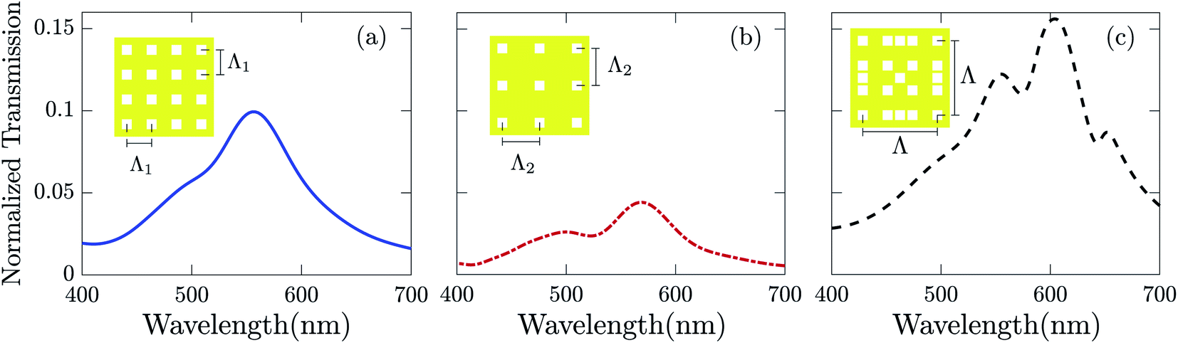 | ||
| Fig. 3 Normalized transmission spectra of bare metal square NHAs with periodicities (a) 250 nm and (b) 375 nm. (c) Normalized transmission of a bare metal merged lattice square NHA with periodicity 750 nm. The Au NHA schematic diagrams are shown in insets. | ||
The increased localization of waves directly results in a better resonator design for the multimode laser as it provides the necessary optical feedback in more than one mode for entrapping light. The designed merged lattice NHA for this structure incorporates better localization than a simple periodic system. The hole arrangement in the merged lattice is pseudo-random, as there is randomness on the short scale but a fixed periodicity on the longer scale. In this work, the simple lattices have been chosen such that they differ slightly in spatial resonances, which coalesce together to form 2D spatial beats.39 We show the transmission spectra of the designed merged lattice NHA in Fig. 3(c). The dual-mode lasing is sensitive to the hole dimensions and periodicity of the metal NHA. Therefore, they must be designed meticulously as the dual-mode lasing might cease to exist if the cavity mode is not supported by the gain lineshape. Also, our objective is to keep the lateral dimensions of the primitive unit cell to a minimum.
To keep the surface plasmon modes close to the emission peak of the gain medium, the ratio of the two short-scale periods r was selected to be 3/2, making R = 3 and Λ = 750 nm. If R is an integer greater than 3, we get Λ > 750 nm, as Λ increases linearly with R when Λ1 is a constant. We have kept R to a minimum possible value as greater values would make the structure laterally larger. Additionally, an increase in R will make the surface plasmon resonance (SPR) wavelength elude the vicinity of the gain medium emission peak, as the SPR is sensitive to Λ. To keep the lateral span of the merged lattice unit cell constant for increasing R, Λ1 could be reduced. However, a smaller Λ1 has a negative effect on the overall transmission intensity of the structure as the SPR shows a blue-shift when Λ1 decreases. Thus, Λ1 = 250 nm and Λ2 = 375 nm are the optimum parameter values that resulted in the best possible emission characteristics.
To investigate the resonant radiative modes of the optical cavity, we consider the gain medium as a passive layer, i.e., the PU host matrix is devoid of dye molecules. We calculate the passive optical cavity's transmission spectra for an incident broad-band plane wave. The transmission spectra of the passive cavity with simple and merged lattice NHAs are shown in Fig. 4. While a single radiative mode is obtained in the transmission spectra for structures with simple NHAs, dual radiative modes are observed in the transmission spectra for the structure with the merged lattice NHA. We find that the EOT modes obtained from the bare merged lattice metal NHA, as presented in Fig. 3(c), are red-shifted to 860 and 864 nm in Fig. 4(d). The shifts in mode wavelengths are due to the change of SPR of the bare Au NHA to TP resonances in the passive optical cavity with a DBR. The red-shift of the plasmonic mode also becomes apparent due to the increase of the effective index when the DBR is attached to the PU layer. In the proposed structure, alternating layers of TiO2 and MgF2 act as a DBR, producing a band-gap stretching from ∼840 nm to ∼1200 nm, as shown in the normalized reflection spectrum of the DBR in Fig. 4(d).
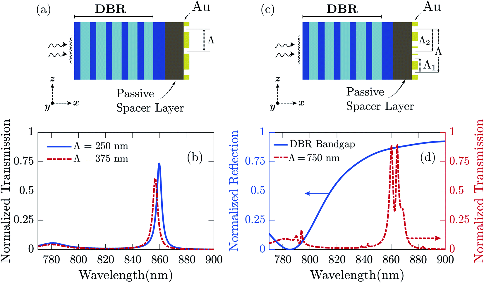 | ||
| Fig. 4 (a) Passive cavity structure with a simple periodic Au NHA. The simple NHA has a periodicity of Λ. (b) Transmission spectra for the structure in (a) with Λ = 250 and 375 nm. (c) Passive cavity structure with a merged lattice Au NHA. The merged lattice NHA has a periodicity of Λ = 3Λ1 = 2Λ2, where Λ1 = 250 nm and Λ2 = 375 nm. (d) Transmission spectrum of the structure in (c) and the lower band-edge of the reflection spectrum of the isolated DBR shown in the schematic diagrams in (a) and (c). | ||
We note that when the DBR is attached to the PU layer to make an optical cavity, the reflection spectrum significantly changes from that of the bare DBR. The incident light couples to TP modes at the Au–PU dielectric interface, and intense transmission peaks are obtained within the photonic band-gap of the DBR. In the proposed structure, the transmission peak wavelengths overlap with the gain bandwidth of IR-140 dye molecules. Fig. 5 shows the excited modes in the transverse and longitudinal cross-sectional planes of the passive cavity. The transverse Au–PU interface shows a high field intensity and localization at the hole edges—the shorter wavelength mode is localized at the corner hole edges, as shown in Fig. 5(b), and the longer wavelength mode is localized at the central hole edges, as shown in Fig. 5(c). The field intensities in the longitudinal cross-sectional plane along the resonant hole edges are plotted in Fig. 5(d) and (e). The  -field intensity amplification at the metal–PU layer interface, and the
  -field intensity distribution in the cavity signify the excitation of TP modes.52,55,56 To ensure a proper resonator response for the design, the TP resonance was designed to be around 870 nm for the maximum gain. Therefore, the period span and hole dimensions of the Au–NHA have been optimized and minimized so that the cavity modes fall within the span of ∼100 nm gain medium linewidth around the peak at 870 nm. As band-edge states offer a higher quality response and better wave localization,36 the DBR has been designed to have its first band-edge close to the position of the TP wavelength and gain emission wavelength at around 870 nm.
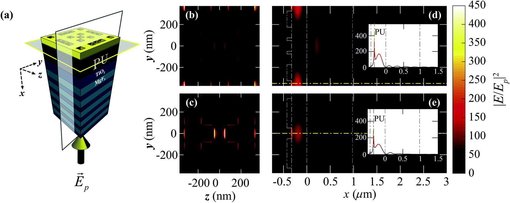 | ||
Fig. 5 (a) Passive optical cavity of the proposed laser along with the cross-sectional planes in which electric field profiles have been analyzed. The cavity is normally excited by a broad-band plane wave source  . The normalized electric field intensity . The normalized electric field intensity  profiles in the transverse y–z cross-sectional plane at (b) 860 nm and (c) 865 nm. profiles in the transverse y–z cross-sectional plane at (b) 860 nm and (c) 865 nm.  profiles in the longitudinal x–y cross-sectional plane taken at the z-value at the resonant hole edges for (d) 860 nm and (e) 865 nm. In the insets of (d) and (e), profiles in the longitudinal x–y cross-sectional plane taken at the z-value at the resonant hole edges for (d) 860 nm and (e) 865 nm. In the insets of (d) and (e),  are plotted along the x-directional line-section through the center of the structure in the y-direction. are plotted along the x-directional line-section through the center of the structure in the y-direction. | ||
4.2 Dual mode lasing and an ultra-low threshold
Fig. 6 shows the near-field emission spectra and output versus pump pulse intensity when the PU layer is doped with IR-140 dye molecules. Fig. 6(b) shows the lasing spectra for the designed plasmonic laser except for the merged lattice metal NHA replaced by a simple metal NHA. For both Λ = 250 and 375 nm, the lasing emission occurs in a single mode with peaks at 870 and 867 nm, respectively. By contrast, we note that the emission occurs in two isolated wavelength modes with peaks at ∼869 nm and ∼879 nm for two different incident pump energy (Ep) values, as shown in Fig. 6(c) and (d). The resonances can be attributed to two distinct plasmon modes excited due to the merged lattice metal NHA. We note that the lasing modes in Fig. 6(d) are slightly red-shifted from that of the passive cavity, as presented in Fig. 4(d), which can be explained by the interaction of cavity modes with dye molecules placed within the cavity. Isolated dye molecules, in the absence of any cavity, would radiate at a different wavelength than when placed within a plasmonic cavity. The wavelength shift happens because of the quantum electrodynamics associated with the atom-cavity coupling introducing a frequency pulling effect.57–59 The gain profile of IR-140 is centered at 870 nm and has a linewidth of ∼100 nm,60 which is broad enough to support both the lasing modes.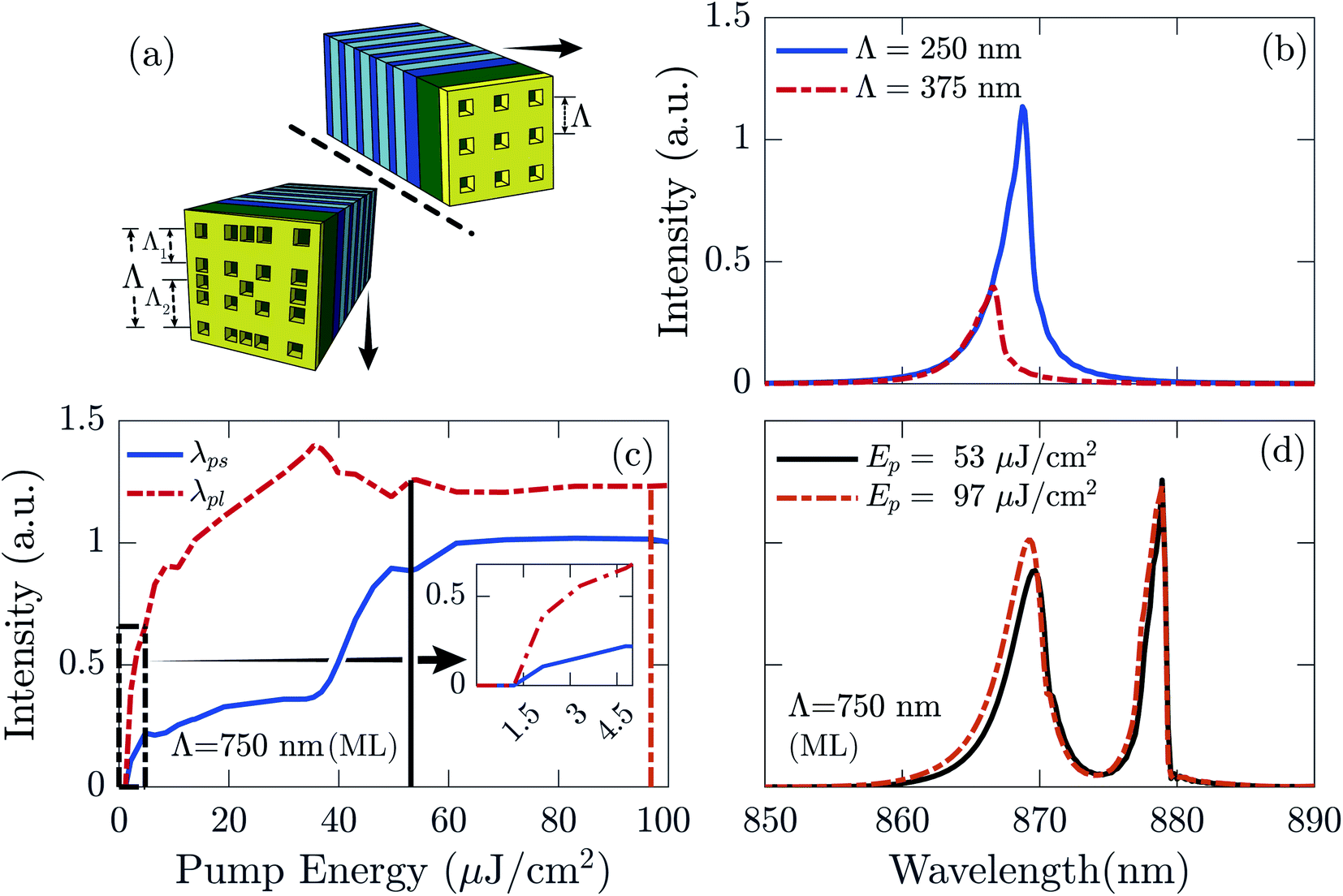 | ||
| Fig. 6 (a) Schematic diagrams of the laser structure with simple (upper right) and merged lattice (lower left) metal NHAs. (b) Single-mode lasing emission from the simple lattice metal NHA based laser for Λ = 250 and 375 nm. (c) Peak intensities of the smaller (λps) and longer wavelength (λpl) modes vs. pump energy of the merged lattice metal NHA, with the inset showing the threshold pump energy at 1.20 μJ cm−2. (d) Dual-mode lasing emission of the proposed merged lattice NHA based laser structure for two different pump energies (Ep). | ||
To determine whether the emission modes are lasing modes, we have investigated the input vs. output characteristics of our designed merged lattice plasmonic laser. The existence of a threshold pump energy for emission can prove that the emission modes are indeed lasing modes. Therefore, we have varied the incident pump pulse energy and calculated the peak emission intensity, as shown in Fig. 6(c). We note that the designed plasmonic laser does not show any emission when the pump pulse energy is less than 1.20 μJ cm−2. On the contrary, the laser emits dual modes simultaneously after the pump energy crosses the threshold value. Such a dependence of both the output emission modes on the input pump energy suggests that both the emission modes are lasing modes.
The addition of a merged lattice NHA in the proposed dual-mode plasmonic laser has significantly reduced the threshold pump energy over its simple periodic counterpart. The threshold pump energy for the proposed dual-mode laser is an order of magnitude smaller than the reported 13 μJ cm−2 for the planar single-mode plasmonic laser.21 Enhanced localization induced by the merged lattice metal NHA has reduced the threshold value of our laser. Thus, the proposed structure exhibits at least two orders of magnitude improvement in the threshold characteristics over state-of-the-art dual-mode plasmonic lasers, as summarized in Table 2. The changes in emission intensities for the smaller (λps) and longer wavelengths (λpl) show similar trends when the pump energy is ∼35 μJ cm−2. However, the λpl mode has a greater intensity than the λps mode. Above the threshold value, at first, both mode intensities increase with increasing pump energy at a high rate. We note that the lasing at the longer wavelength, which corresponds to the smaller transition energy, experiences gain saturation when the pump energy increases to ∼40 μJ cm−2. Therefore, at ∼40 μJ cm−2, the smaller lasing wavelength has more gain available, and it grows in intensity. However, for a pump energy of ∼60 μJ cm−2, the lasing emission intensities are almost saturated for both modes.
We show normalized electric field intensity  profiles in the transverse and vertical cross-sections of the plasmonic laser structure in Fig. 7. In the transverse cross-section along the metal–gain medium interface, the
  profile shows that plasmonic modes are excited at the corner holes of a unit cell at the smaller wavelength λps, as shown in Fig. 7(b). By contrast, plasmonic modes are excited at the central holes of a unit cell at the longer wavelength λpl, as shown in Fig. 7(c). The incident plane wave is polarized along the z-direction, and the spatial modes are excited perpendicular to the direction of incidence. The SPP mode is also excited along the hole edge. Since the holes are 100 nm in size, neighboring holes along the edges of a unit cell are only separated by 25 nm. Therefore, LSPs in two neighboring holes across such a small distance couple and form stronger modes. In Fig. 7(d) and (e), we show
  profiles at 869 nm and 879 nm wavelengths, respectively, in the vertical cross-section along the x-direction of the structure as indicated by the vertical section plane (black border) in Fig. 7(a). We observe that plasmonic modes are excited at the hole edges along the metal–gain medium interface.
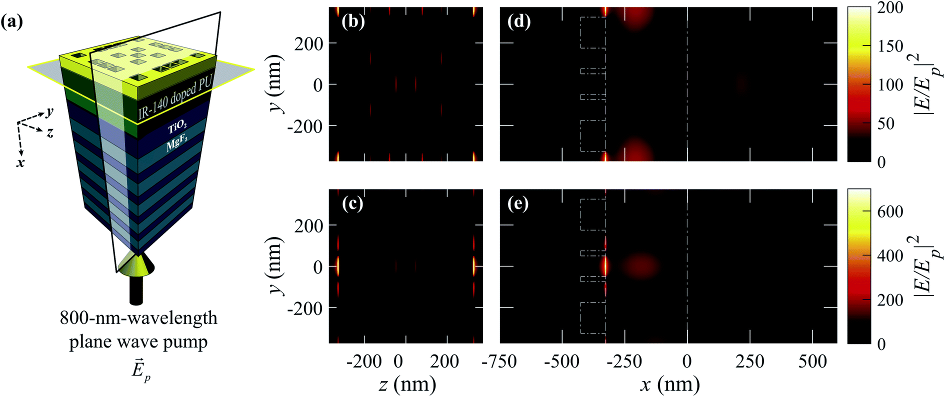 | ||
Fig. 7 (a) Schematic diagram of the proposed laser structure and cross-sectional planes along which the field profiles are analyzed. The laser is optically pumped by an 800 nm-wavelength plane wave pulse  . Normalized . Normalized  -field profile in the transverse y–z cross-sectional plane at the Au–gain medium interface for (b) λps = 869 nm and (c) λpl = 879 nm. Normalized -field profile in the transverse y–z cross-sectional plane at the Au–gain medium interface for (b) λps = 869 nm and (c) λpl = 879 nm. Normalized  -field intensity profile in the longitudinal x–y cross-sectional plane calculated at the z-value of the resonant hole edges at lasing wavelengths (d) λps = 869 nm and (e) λpl = 879 nm. The lasing -field intensity profile in the longitudinal x–y cross-sectional plane calculated at the z-value of the resonant hole edges at lasing wavelengths (d) λps = 869 nm and (e) λpl = 879 nm. The lasing  -field is normalized by the pump pulse -field is normalized by the pump pulse  . . | ||
4.3 Lasing emission dynamics
The results of the near-field mode dynamics are presented in Fig. 8 and 9. Fig. 8(a) shows the lasing emission for two sets of N and dL values: (1) N = 5 and dL = 200 nm and (2) N = 9 and dL = 180 nm. In each case, the proposed laser emits intense and distinct dual modes. However, for two different sets of N and dL values: (1) N = 5 and dL = 170 nm and (2) N = 11 and dL = 216 nm, the proposed laser does not show distinct dual modes, as shown in Fig. 8(b). For the first case, although the modes are spectrally distinct, the smaller wavelength mode is too broad and weak to be usable. By contrast, for the second case, the lasing modes are so close to each other that their spectral overlap creates a distorted mode shape, and they can no longer be distinguished as isolated modes. Therefore, to define practicable dual-mode emissions and find a tuning range of the proposed laser, we consider the emission intensity at N = 5 and dL = 200 nm in Fig. 8(a) as a reference to define the dual-mode emissions. This particular configuration of N and dL gives us clear, well-separated, and almost equally-prominent peak intensities, as will become clear in the results presented in the following paragraphs. We assume that if the peak intensity of any mode becomes less than 0.2 times the peak intensity at N = 5 and dL = 200 nm, the emission is too weak and less than the minimum acceptable value. On the other hand, if the separation between the two lasing modes is smaller than their combined linewidths, the modes significantly overlap and result in a distorted single-mode, with possible adjacent side lobes. Such a case of distorted mode shape is also not considered as dual-mode lasing.
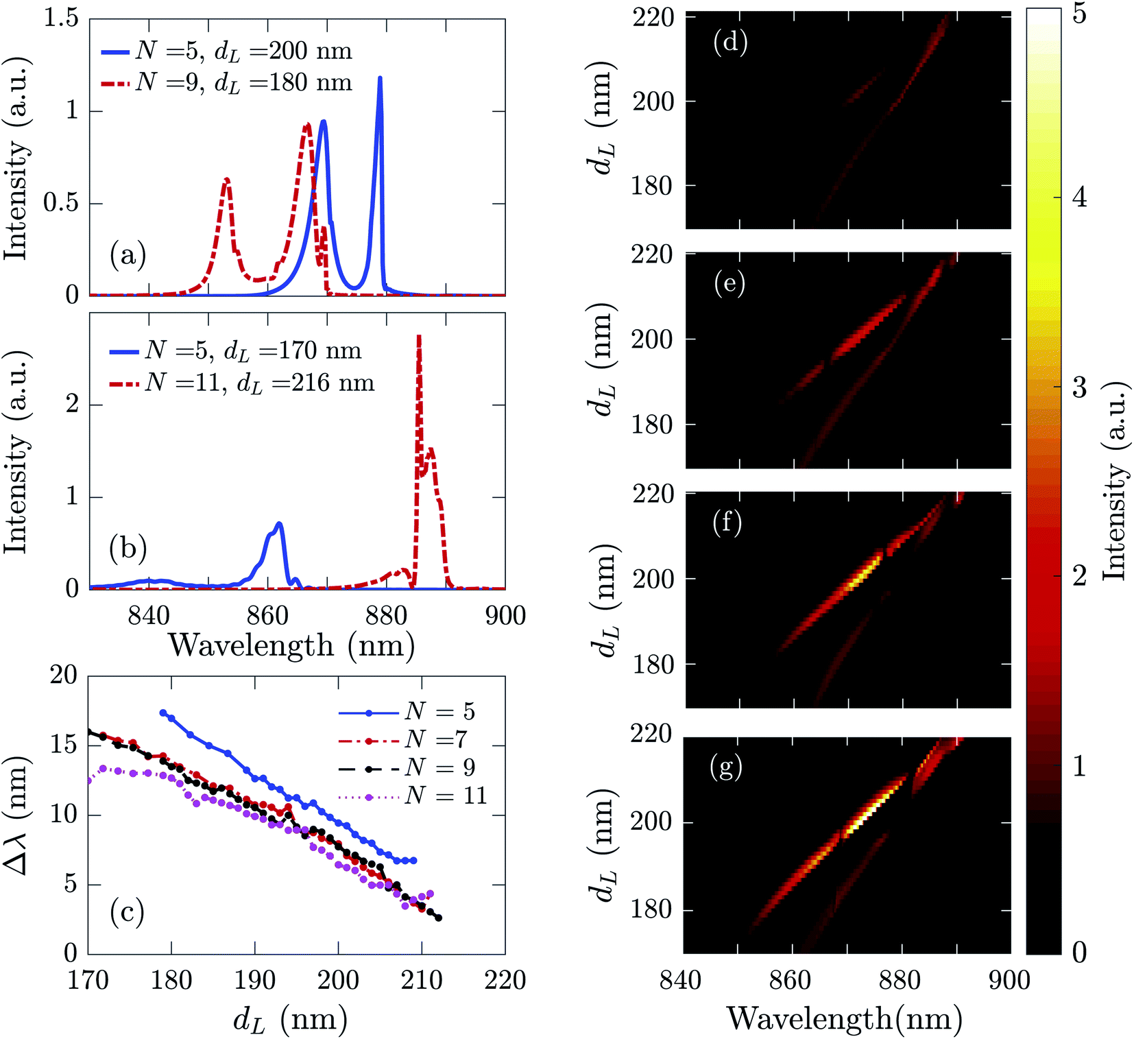 | ||
| Fig. 8 (a) Emission intensity spectra for two sets of DBR TiO2–MgF2 pair number (N) and the terminating TiO2 layer thickness (dL), showing intense and distinct dual-mode lasing. (b) Emission intensity spectra for two different sets of N and dL from those in (a), showing too weak or overlapped and distorted lasing modes. (c) Separation between the lasing modes (Δλ) as a function of dL for different N values. 2D surface plots of the peak emission intensities vs. wavelength and dL for (d) N = 5, (e) N = 7, (f) N = 9, and (g) N = 11. | ||
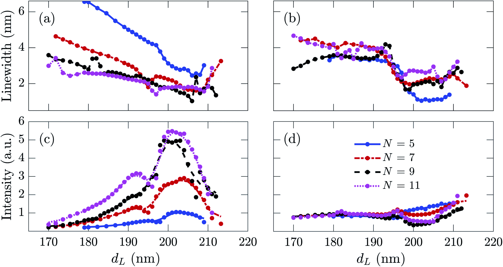 | ||
| Fig. 9 FWHM linewidths of the (a) smaller wavelength lasing mode and (b) longer wavelength lasing mode as functions of dL for different N. Peak emission intensities of the (c) smaller wavelength lasing mode and (d) longer wavelength mode as functions of dL for different N. | ||
The mode intensities, peak wavelengths, separations, and linewidths vary when N and dL change. We find that the mode separation (Δλ) of the lasing modes shows a non-monotonic dependence on N and dL, as shown in Fig. 8(c). When dL increases with a fixed N, we find that Δλ decreases. Similarly, Δλ shows a decreasing trend as N increases. Because of the complex geometry of the merged lattice NHA and the mode competition between the lasing modes, the output behavior is substantially non-linear. Fig. 8(d)–(g) show 2D surface plots for the emission intensity of the proposed laser against wavelength and dL. The proposed structure can be tuned to emit in the smaller wavelength mode in the range of ∼845–883 nm and in the longer wavelength mode in the range of ∼860–886 nm by changing dL and N. When dL ≳ 210 nm for any N, we find that Δλ becomes too small to support the linewidth of the two individual modes, and the dual modes get distorted and become indistinguishable due to the spectral overlap. With a decreasing Δλ, the dual modes merge and emerge as a broader and distorted single mode.
Fig. 9 shows the full-width at half-maximum (FWHM) linewidths and peak intensities of the two wavelength modes when dL varies between 160 and 220 nm for N = 5, 7, 9, and 11. FWHM linewidths show a non-monotonic decreasing trend with dL, especially for the smaller wavelength mode, as shown in Fig. 9(a) and (b). When N = 5, the smaller wavelength mode has a broader linewidth compared to that of the longer wavelength mode. However, for N > 5, the smaller wavelength mode has a narrower linewidth than that of the longer wavelength mode for a significant range of dL. The smaller wavelength mode's linewidth decreases with increasing N, while the longer wavelength mode's linewidth shows a less significant variation with N.
Fig. 9(c) and (d) show the intensities of the lasing modes against dL for different N. For N = 5 and 7, the two wavelength modes are in significantly good shape and of similar relative prominence in intensity. However, for N = 9 and 11, we get a much greater intensity for the smaller wavelength mode compared to that of the longer wavelength mode, especially when dL varies in the range of ∼195–210 nm. Fig. 9(c) and (d) show that the peak intensity of the smaller wavelength mode has a maximum around dL ≈ 200 nm and increases non-monotonically with N. The longer wavelength mode shows only a little variation in its peak intensity. We note that a greater N favors stronger emissions from the smaller wavelength mode, making it more prominent than the longer wavelength mode. The peak intensity and linewidth of the longer wavelength mode remain almost unaffected with the change of N.
The tendencies of the separation, spectral position, linewidth, and peak intensities of the two lasing modes presented in Fig. 8 and 9 primarily depend on the physics of the tuning mechanism of TP modes for varying dL and N. The trends observed in the near-field mode dynamics conform to the existing theoretical formulations of Tamm resonance behavior at the metal–DBR interface.50,61 A 1D “double period” patterning of the top metal layer has been shown to create a Tamm plasmonic band-gap with two modes and control their tuning characteristics.64 The merged lattice metal NHA on top of the gain medium also contributes to the tuning behaviour besides exciting Tamm resonances. Through such an in-depth analysis of the lasing mode dynamics, we have determined a range of values for N and dL that would create an intense and spectrally well-separated dual-mode emission. The calculated ranges for limiting structural parameter values for dual-mode lasing are given in Table 3. Within these ranges, the intensities of the lasing modes are high and comparable to those of other reported plasmonic lasers; the linewidths are narrow, and the lasing modes do not overlap each other.
| N | 5 | 7 | 9 | 11 |
| d L | ∼179–209 nm | ∼171–213 nm | ∼170–211 nm | ∼170–212 nm |
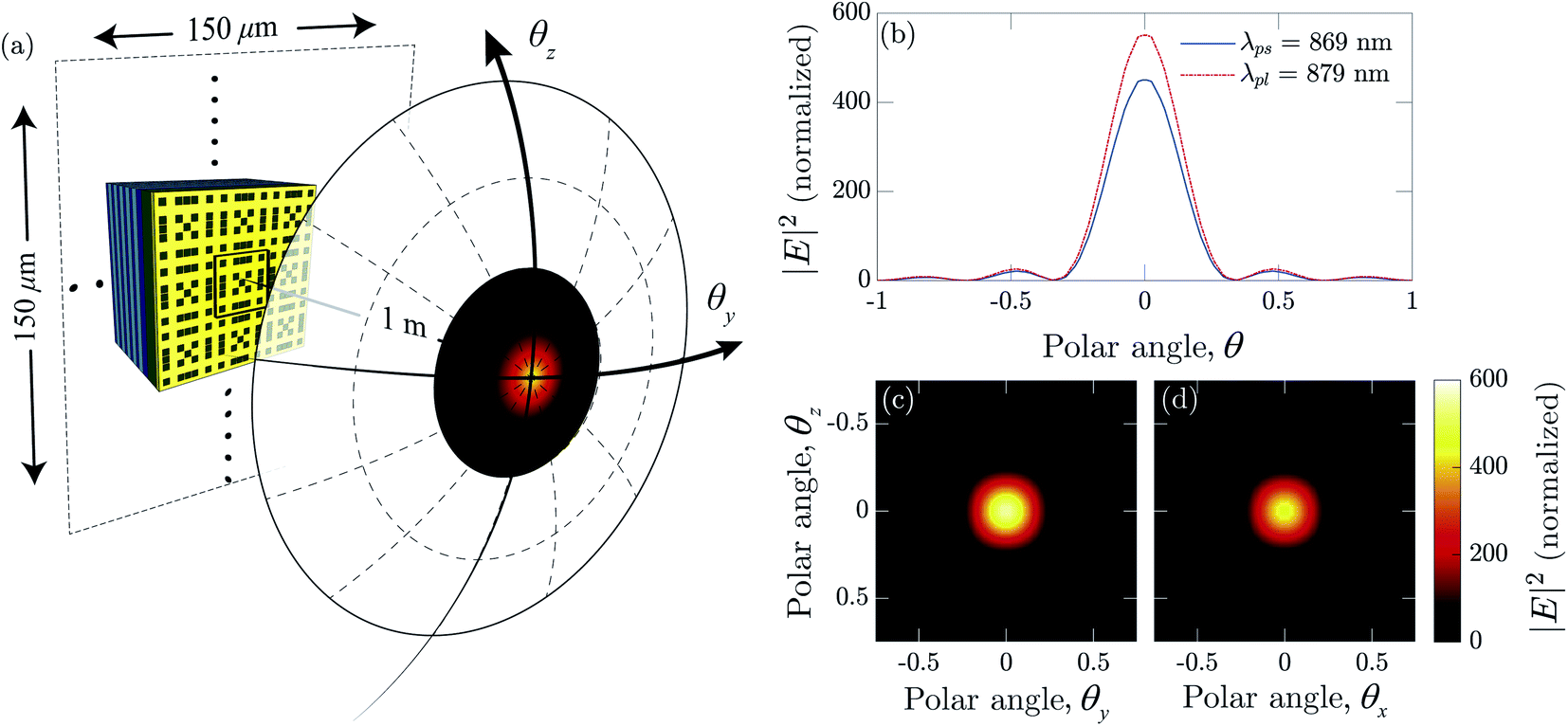 | ||
Fig. 10 (a) Schematic diagram of the proposed merged lattice laser structure along with a portion of the hemispherical detection plane at a distance of 1 m away from the near-field detection plane for angle resolved far-field projection of EM fields. The near-field detection plane is indicated by the rectangle close to the metal film. (b) Far-field  -field intensity distribution normalized to that of a free space pump beam versus the polar angle at 0° azimuth. 2D polar spatial normalized far-field intensity for the (c) λps = 869 nm lasing mode and (d) λpl = 879 nm lasing mode. -field intensity distribution normalized to that of a free space pump beam versus the polar angle at 0° azimuth. 2D polar spatial normalized far-field intensity for the (c) λps = 869 nm lasing mode and (d) λpl = 879 nm lasing mode. | ||
We have calculated the far-field patterns of the proposed merged lattice plasmonic laser for a device area of 150 μm × 150 μm in the yz-plane. The far-field intensity profile is obtained by projecting the near-field profile away to a distance of 1 m. Then the obtained far-field distribution profiles have been normalized using the intensity of the pump pulse. The far-field analyses for both the lasing modes show similar results, as shown in Fig. 10. The long-range periodicity of the lattice and the two-fold symmetry in the merged lattice configuration cause a more significant constructive interference in the far field. The proposed laser produces a far-field divergence angle of <0.35°, which is much smaller than that of other dual-mode plasmonic lasers.36–38 The far-field divergence angle of the proposed laser is also significantly smaller than the reported 1° divergence angle of the planar single-mode laser in ref. 21. Therefore, the addition of a merged lattice NHA has notably improved the performance of our dual-mode plasmonic laser in the far field compared to the planar single-mode laser in ref. 21 and dual-mode lasers reported in ref. 36–38. Our design is thus highly coherent in the near-field spatial domain and directional in the far field.
5 Conclusion
In conclusion, a merged lattice metal NHA plasmonic laser has been designed and theoretically demonstrated to produce dual-mode lasing. The merged lattice NHA produces EOT of the excited plasmonic modes by gain emissions. The two-fold periodicity in the merged lattice NHA creates dual plasmonic resonances that support two output transmission modes. By carefully designing the merged lattice NHA, we find an overlap of the transmission peaks with the gain spectrum of IR 140 molecules. The merged lattice also creates scattering loops within the gain medium, increasing light confinement at multiple modes and thus reducing the threshold pump energy by at least two orders of magnitude from state-of-the-art dual-mode plasmonic laser demonstrations. The lasing wavelength of the proposed dual-mode laser is tunable over a broad range of ∼845–886 nm by changing structural parameters. The sub-wavelength nanohole dimensions and periodicity in the metal layer produce only the zeroth-order spatial mode in the far field, getting rid of the higher order modes, and thereby producing a highly converged far-field pattern. The intense and isolated dual lasing modes of the proposed laser, with an ultra-low threshold pump energy and highly converged far-field pattern, can be critically important for many envisioned and crucial applications.Author contributions
M. A. Talukder defined the research goal and initial concept of the work and supervised the research work. S. Shahid and S.-E-Zumrat developed the detailed concept and the theoretical and simulation models, and performed the simulation and analysis. All three authors contributed to the data visualization and preparation of the manuscript.Conflicts of interest
The authors declare no conflicts of interest.References
- L. Novotny and S. J. Stranick, Near-field optical microscopy and spectroscopy with pointed probes, Annu. Rev. Phys. Chem., 2006, 57(1), 303–331 CrossRef CAS PubMed.
- T. W. Johnson, Z. J. Lapin, R. Beams, N. C. Lindquist, S. G. Rodrigo, L. Novotny and S.-H. Oh, Highly reproducible near-field optical imaging with sub-20-nm resolution based on template-stripped gold pyramids, ACS Nano, 2012, 6(10), 9168–9174 CrossRef CAS PubMed.
- L. Novotny and B. Hecht, Principles of Nano-Optics, Cambridge University Press, 2006 Search PubMed.
- M. I. Stockman, Nanoplasmonic sensing and detection, Science, 2015, 348(6232), 287–288 CrossRef CAS PubMed.
- M. I. Stockman, K. Kneipp, S. I. Bozhevolnyi, S. Saha, A. Dutta, J. Ndukaife, N. Kinsey, H. Reddy, U. Guler, V. M. Shalaev, A. Boltasseva, B. Gholipour, H. N. S. Krishnamoorthy, K. F. MacDonald, C. Soci, N. I. Zheludev, V. Savinov, R. Singh, P. Groß, C. Lienau, M. Vadai, M. L. Solomon, D. R. Burton III, M. Lawrence, J. A. Dionne, S. V. Boriskina, R. Esteban, J. Aizpurua, X. Zhang, S. Yang, D. Wang, W. Wang, T. W. Odom, N. Accanto, P. M. d. Roque, I. M. Hancu, L. Piatkowski, N. F. v. Hulst and M. F. Kling, Roadmap on plasmonics, J. Opt., 2018, 20(4), 043001 CrossRef.
- J. A. Schuller, E. S. Barnard, W. Cai, Y. C. Jun, J. S. White and M. L. Brongersma, Plasmonics for extreme light concentration and manipulation, Nat. Mater., 2010, 9(3), 193–204 CrossRef CAS PubMed.
- R.-M. Ma and R. F. Oulton, Applications of nanolasers, Nat. Nanotechnol., 2019, 14(1), 12–22 CrossRef CAS PubMed.
- M. Stockman, Spasers to speed up CMOS processors, US Pat., 10096675, 2018 Search PubMed.
- Z. Xie, W. Yu, T. Wang, H. Zhang, Y. Fu, H. Liu, F. Li, Z. Lu and Q. Sun, Plasmonic nanolithography: A review, Plasmonics, 2011, 6(3), 565 CrossRef.
- M. Fedoruk, M. Meixner, S. Carretero-Palacios, T. Lohmüller and J. Feldmann, Nanolithography by plasmonic heating and optical manipulation of gold nanoparticles, ACS Nano, 2013, 7(9), 7648–7653, DOI:10.1021/nn402124p , pMID: 23941522, .
- W. Srituravanich, N. Fang, C. Sun, Q. Luo and X. Zhang, Plasmonic nanolithography, Nano Lett., 2004, 4(6), 1085–1088 CrossRef CAS.
- S. Kawata, Y. Inouye and P. Verma, Plasmonics for near-field nano-imaging and superlensing, Nat. Photonics, 2009, 3(7), 388–394 CrossRef CAS.
- J. N. Anker, W. P. Hall, O. Lyandres, N. C. Shah, J. Zhao and R. P. V. Duyne, Biosensing with plasmonic nanosensors, Nat. Mater., 2008, 7(6), 442–453 CrossRef CAS PubMed.
- J. Homola, Surface plasmon resonance sensors for detection of chemical and biological species, Chem. Rev., 2008, 108(2), 462–493 CrossRef CAS PubMed.
- D. J. Bergman and M. I. Stockman, Surface plasmon amplification by stimulated emission of radiation: quantum generation of coherent surface plasmons in nanosystems, Phys. Rev. Lett., 2003, 90(2), 027402 CrossRef PubMed.
- E. S. Andrianov, A. A. Pukhov, A. V. Dorofeenko and A. P. Vinogradov, Spaser operation in the presence of external optical field, J. Commun. Technol. Electron., 2012, 57(1), 106–116 CrossRef.
- D. Li and M. I. Stockman, Electric spaser in the extreme quantum limit, Phys. Rev. Lett., 2013, 110(10), 106803 CrossRef PubMed.
- C. Jayasekara, M. Premaratne, S. D. Gunapala and M. I. Stockman, Mos2 spaser, J. Appl. Phys., 2016, 119(13), 133101 CrossRef.
- Y. Huo, T. Jia, T. Ning, C. Tan, S. Jiang, C. Yang, Y. Jiao and B. Man, A low lasing threshold and widely tunable spaser based on two dark surface plasmons, Sci. Rep., 2017, 7(1), 13590 CrossRef PubMed.
- J.-S. Wu, V. Apalkov and M. I. Stockman, Topological spaser, Phys. Rev. Lett., 2020, 124(1), 017701 CrossRef CAS PubMed.
- Z. Ahmed and M. A. Talukder, An efficient and directional optical Tamm state assisted plasmonic nanolaser with broad tuning range, J. Phys. Commun., 2018, 2(4), 045016 CrossRef.
- Z. Azad and M. A. Talukder, Simultaneously surface- and edge-emitting plasmonic laser operating in the near-infrared region, Opt. Laser Technol., 2022, 146, 107571 CrossRef.
- R. Gaulton, F. Danson, F. Ramirez and O. Gunawan, The potential of dual-wavelength laser scanning for estimating vegetation moisture content, Remote Sens. Environ., 2013, 132, 32–39 CrossRef.
- G. David, A. Miffre, B. Thomas and P. Rairoux, Sensitive and accurate dual-wavelength UV-vis polarization detector for optical remote sensing of tropospheric aerosols, Appl. Phys. B: Lasers Opt., 2012, 108(1), 197–216 CrossRef CAS.
- K. Meiners-Hagen, R. Schödel, F. Pollinger and A. Abou-Zeid, Multi-wavelength interferometry for length measurements using diode lasers, Meas. Sci. Rev., 2009, 9(1), 16–26 Search PubMed.
- R. Dändliker, R. Thalmann and D. Prongué, Two-wavelength laser interferometry using superheterodyne detection, Opt. Lett., 1988, 13(5), 339 CrossRef PubMed.
- N. Pleros, E. E. Kriezis and K. Vyrsokinos, Optical interconnects using plasmonics and si-photonics, IEEE Photonics J., 2011, 3(2), 296–301 Search PubMed.
- A. Christ, S. G. Tikhodeev, N. A. Gippius, J. Kuhl and H. Giessen, Waveguide-plasmon polaritons: strong coupling of photonic and electronic resonances in a metallic photonic crystal slab, Phys. Rev. Lett., 2003, 91(18), 183901 CrossRef CAS PubMed.
- M. Stucchi, S. Cosemans, J. V. Campenhout, Z. Tőei and G. Beyer, On-chip optical interconnects versus electrical interconnects for high-performance applications, Microelectron. Eng., 2013, 112, 84–91 CrossRef CAS.
- D. Ozcelik, J. W. Parks, T. A. Wall, M. A. Stott, H. Cai, J. W. Parks, A. R. Hawkins and H. Schmidt, Optofluidic wavelength division multiplexing for single-virus detection, Proc. Natl. Acad. Sci. U. S. A., 2015, 112(42), 12933–12937 CrossRef CAS PubMed.
- K. Ohashi, H. Yukawa, M. Kinoshita, N. Suzuki, A. Gomyo, T. Ishi, D. Okamoto, K. Furue, T. Ueno, T. Tsuchizawa, T. Watanabe, K. Nishi, K. Yamada, S.-i. Itabashi, J. Akedo, T. Shimizu, M. Nakada, J. Fujikata, J. Ushida, S. Torii, K. Nose and M. Mizuno, On-chip optical interconnect, Proc. IEEE, 2009, 97(7), 1186–1198 CAS.
- K. Koo and A. Kersey, Bragg grating-based laser sensors systems with interferometric interrogation and wavelength division multiplexing, J. Lightwave Technol., 1995, 13(7), 1243–1249 CrossRef.
- A. Tredicucci, C. Gmachl, F. Capasso, D. L. Sivco, A. L. Hutchinson and A. Y. Cho, A multiwavelength semiconductor laser, Nature, 1998, 396(6709), 350–353 CrossRef CAS.
- N. K. Dutta, T. Cella, J. L. Zilko, D. A. Ackerman, A. B. Piccirilli and L. I. Greene, InGaAsP closely spaced dual wavelength laser, Appl. Phys. Lett., 1986, 48(25), 1725–1726, DOI:10.1063/1.96815.
- K. J. Beernink, R. L. Thornton and H. F. Chung, Low threshold current dual wavelength planar buried heterostructure lasers with close spatial and large spectral separation, Appl. Phys. Lett., 1994, 64(9), 1082–1084, DOI:10.1063/1.110939.
- D. Wang, A. Yang, W. Wang, Y. Hua, R. D. Schaller, G. C. Schatz and T. W. Odom, Band-edge engineering for controlled multi-modal nanolasing in plasmonic superlattices, Nat. Nanotechnol., 2017, 12(9), 889–894 CrossRef CAS PubMed.
- S. Pourjamal, T. K. Hakala, M. Nečada, F. Freire-Fernández, M. Kataja, H. Rekola, J.-P. Martikainen, P. Törmä and S. v. Dijken, Lasing in ni nanodisk arrays, ACS Nano, 2019, 13(5), 5686–5692 CrossRef CAS PubMed.
- J. M. Winkler, M. J. Ruckriegel, H. Rojo, R. C. Keitel, E. D. Leo, F. T. Rabouw and D. J. Norris, Dual-wavelength lasing in quantum-dot plasmonic lattice lasers, ACS Nano, 2020, 14(5), 5223–5232 CrossRef CAS PubMed.
- G. Alagappan and C. E. Png, Localization of waves in merged lattices, Sci. Rep., 2016, 6(1), 31620 CrossRef CAS PubMed.
- S.-H. Chang and A. Taflove, Finite-difference time-domain model of lasing action in a four-level two-electron atomic system, Opt. Express, 2004, 12(16), 3827 CrossRef PubMed.
- M. Dridi and G. C. Schatz, Model for describing plasmon-enhanced lasers that combines rate equations with finite-difference time-domain, J. Opt. Soc. Am. B, 2013, 30(11), 2791 CrossRef CAS.
- A. Degiron and T. W. Ebbesen, The role of localized surface plasmon modes in the enhanced transmission of periodic subwavelength apertures, J. Opt. A: Pure Appl. Opt., 2005, 7(2), S90–s96 CrossRef.
- T. W. Ebbesen, H. J. Lezec, H. F. Ghaemi, T. Thio and P. A. Wolff, Extraordinary optical transmission through sub-wavelength hole arrays, Nature, 1998, 391(6668), 667–669 CrossRef CAS.
- H. A. Bethe, Theory of diffraction by small holes, Phys. Rev., 1944, 66(7–8), 163–182 CrossRef.
- C. J. Bouwkamp, “Diffraction theory,”, Rep. Prog. Phys., 1954, 17(1), 35 CrossRef.
- K. J. K. Koerkamp, S. Enoch, F. B. Segerink, N. F. v. Hulst and L. Kuipers, Strong influence of hole shape on extraordinary transmission through periodic arrays of subwavelength holes, Phys. Rev. Lett., 2004, 92(18), 183901 CrossRef PubMed.
- X. Shou, A. Agrawal and A. Nahata, Role of metal film thickness on the enhanced transmission properties of a periodic array of subwavelength apertures, Opt. Express, 2005, 13(24), 9834 CrossRef PubMed.
- X. Zhang, G. Liu, Z. Liu, Z. Cai, Y. Hu, X. Liu, G. Fu, H. Gao and S. Huang, Effects of compound rectangular subwavelength hole arrays on enhancing optical transmission, IEEE Photonics J., 2015, 7(1), 1–8 Search PubMed.
- P. W. Anderson, Absence of diffusion in certain random lattices, Phys. Rev., 1958, 109(5), 1492–1505 CrossRef CAS.
- R. Brückner, M. Sudzius, S. I. Hintschich, H. Fröb, V. G. Lyssenko and K. Leo, Hybrid optical Tamm states in a planar dielectric microcavity, Phys. Rev. B: Condens. Matter Mater. Phys., 2011, 83(3), 033405 CrossRef.
- A. V. Kavokin, I. A. Shelykh and G. Malpuech, Lossless interface modes at the boundary between two periodic dielectric structures, Phys. Rev. B: Condens. Matter Mater. Phys., 2005, 72(23), 233102 CrossRef.
- M. Kaliteevski, I. Iorsh, S. Brand, R. A. Abram, J. M. Chamberlain, A. V. Kavokin and I. A. Shelykh, Tamm plasmon-polaritons: possible electromagnetic states at the interface of a metal and a dielectric Bragg mirror, Phys. Rev. B: Condens. Matter Mater. Phys., 2007, 76(16), 165415 CrossRef.
- M. E. Sasin, R. P. Seisyan, M. A. Kalitteevski, S. Brand, R. A. Abram, J. M. Chamberlain, A. Y. Egorov, A. P. Vasil'ev, V. S. Mikhrin and A. V. Kavokin, Tamm plasmon polaritons: slow and spatially compact light, Appl. Phys. Lett., 2008, 92(25), 251112 CrossRef.
- S. Brand, M. A. Kaliteevski and R. A. Abram, Optical Tamm states above the bulk plasma frequency at a Bragg stack/metal interface, Phys. Rev. B: Condens. Matter Mater. Phys., 2008, 79(8), 085416 CrossRef.
- X.-L. Zhang, J.-F. Song, X.-B. Li, J. Feng and H.-B. Sun, Strongly Localized Evanescent Optical Tamm States at Metal-DBR Interface, J. Lightwave Technol., 2012, 31(10), 1654–1659 Search PubMed.
- C. Symonds, S. Azzini, G. Lheureux, A. Piednoir, J. M. Benoit, A. Lemaitre, P. Senellart and J. Bellessa, High quality factor confined Tamm modes, Sci. Rep., 2017, 7(1), 3859 CrossRef CAS PubMed.
- J. J. Sanchez-Mondragon, N. B. Narozhny and J. H. Eberly, Theory of spontaneous emission line shape in an ideal cavity, Phys. Rev. Lett., 1983, 51(20), 1925 CrossRef.
- S. Haroche and D. Kleppner, Cavity quantum electrodynamics, Phys. Today, 1989, 42(1), 24–30 CrossRef CAS.
- M. Moazzezi and Y. V. Rostovtsev, Frequency shift of an optical cavity mode due to a single-atom motion, J. Mod. Opt., 2019, 66(6), 1–5 CrossRef.
- Z. Azad, M. S. Islam and M. A. Talukder, Mode-resolved analysis of a planar multi-layer plasmonic nanolaser, Opt. Commun., 2021, 482, 126614 CrossRef CAS.
- H. Zhou, G. Yang, K. Wang, H. Long and P. Lu, Multiple optical Tamm states at a metal–dielectric mirror interface, Opt. Lett., 2010, 35(24), 4112 CrossRef PubMed.
- B. I. Afinogenov, V. O. Bessonov, A. A. Nikulin and A. A. Fedyanin, Observation of hybrid state of Tamm and surface plasmon-polaritons in one-dimensional photonic crystals, Appl. Phys. Lett., 2013, 103(6), 061112 CrossRef.
- H. Liu, J. Gao, Z. Liu, X. Wang, H. Yang and H. Chen, Large electromagnetic field enhancement achieved through coupling localized surface plasmons to hybrid Tamm plasmons, J. Opt. Soc. Am. B, 2015, 32(10), 2061 CrossRef CAS.
- L. Ferrier, H. S. Nguyen, C. Jamois, L. Berguiga, C. Symonds, J. Bellessa and T. Benyattou, Tamm plasmon photonic crystals: from bandgap engineering to defect cavity, APL Photonics, 2019, 4(10), 106101 CrossRef.
- I. V. Treshin, V. V. Klimov, P. N. Melentiev and V. I. Balykin, Optical Tamm state and extraordinary light transmission through a nanoaperture, Phys. Rev. A: At., Mol., Opt. Phys., 2013, 88(2), 023832 CrossRef.
Footnote |
| † These authors contributed equally. |
| This journal is © The Royal Society of Chemistry 2022 |