
Heterojunction bilayers serving as a charge transporting interlayer reduce the dark current and enhance photomultiplication in organic shortwave infrared photodetectors
Chanho
Shin
a,
Ning
Li
b,
Bogyeom
Seo
b,
Naresh
Eedugurala
 c,
Jason D.
Azoulay
c and
Tse Nga
Ng
*ab
c,
Jason D.
Azoulay
c and
Tse Nga
Ng
*ab
aDepartment of Material Science and Engineering Program, University of California San Diego, 9500 Gilman Drive, La Jolla, CA 92093-0407, USA. E-mail: tnn046@ucsd.edu
bDepartment of Electrical and Computer Engineering, University of California San Diego, 9500 Gilman Drive, La Jolla, CA 92093-0407, USA
cSchool of Polymer Science and Engineering, University of Southern Mississippi, 118 College Drive #5050, Hattiesburg, MS 39406, USA
First published on 25th May 2022
Abstract
Previous approaches to induce photomultiplication in organic diodes have increased the photosignal but lacked control over reducing background noise. This work presents a new interlayer design based on a heterojunction bilayer that concurrently enables photomultiplication and suppresses the dark current in organic shortwave infrared detectors to improve the overall detectivity. The heterojunction bilayer consists of a hole-transporting material copper thiocyanate and an electron-transporting material tin oxide, and this combination offers the ability to block charge injection in the dark. Under illumination, the bilayer promotes trap-assisted photomultiplication by lowering the tunneling barrier and amplifying the photocurrent through the injection of multiple carriers per absorbed photon. Upon incorporating the heterojunction interlayer in photodiodes and upconversion imagers, the devices achieve an external quantum efficiency up to 560% and a detectivity of 3.5 × 10⁹ Jones. The upconversion efficiency of the imager doubles with a 1.7 fold improvement in contrast compared to the imager without the heterojunction interlayer. The new interlayer design is generalizable to work with different organic semiconductors, making it attractive and easy to integrate with emerging organic infrared systems.
New conceptsPhotomultiplication detectors are promising for overcoming the low responsivity in organic shortwave infrared photodetectors. However, recent photomultiplication detectors often increase both the responsivity and dark current, which nullifies the effect on detectivity. To suppress the dark current in photomultiplicative devices, we present a new interlayer structure, a pn junction combination that overcomes the trade-off between signal and noise. Our bilayer design demonstrates the advantages in reduced dark current and excellent external quantum efficiency when compared to devices using typical unipolar charge-transporting materials. We incorporated this new interlayer design in upconversion imagers, doubling the upconversion efficiency and image contrast. This interlayer is generalizable to different organic semiconductors, which are especially useful as the design here will be applicable to future infrared materials yet to be discovered. |
Introduction
Organic photodetectors responsive to shortwave infrared (SWIR) radiation1,2 are an important emerging technology, since organic semiconductors facilitate direct integration and new form factors that can improve the spatial resolution of imagers.3–7 Since the detectivity, namely the signal-to-noise ratio, of organic SWIR detectors is still lower than their conventional inorganic counterparts, recent research has deployed photomultiplication mechanisms to increase the device response.8 In trap-assisted photomultiplication, the charge injection barrier is lowered through an accumulation of photogenerated charges, leading to multiple charges being injected per photon absorbed and resulting in an external quantum efficiency greater than 100%. While successful at amplifying light signals, prior approaches have limited control over reducing dark current noises. To address this challenge, here we examine a new interface design that simultaneously suppresses the dark current9–13 and enables photomultiplication to improve the overall detectivity in organic SWIR devices.Previous organic photomultiplication devices can be categorized into two types, either modifying 1) the bulk heterojunction (BHJ) layer or 2) the charge transporting interlayers next to electrodes. For the first type,14–17 the ratio between donor and acceptor materials is tuned to be dominated by one material ranging from 20![[thin space (1/6-em)]](https://www.rsc.org/images/entities/char_2009.gif) :1 to 100:1; the minor component is isolated from electrodes and serves as trap sites for photogenerated carriers to accumulate, induce band bending, and lower the charge injection barrier. This method of modifying the BHJ layer was acceptable for visible to near-infrared photodiodes. However, for SWIR devices the narrow bandgap materials are less efficient at exciton dissociation18,19 and require a more balanced donor-to-acceptor ratio to reduce recombination loss20 and yield sufficient photogenerated charges to trigger photomultiplication. The second type21–24 of photomultiplication devices, in which interfacial layers are designed to enhance trap-assisted charge injection, does not involve a highly unbalanced BHJ composition and is therefore better suited for SWIR operation. Yet so far, the devices in this second category have been affected by high dark current upon adjustments of interlayer energy levels. Further research on interlayer designs is needed to achieve photomultiplication without a concurrent increase in the dark current.
:1 to 100:1; the minor component is isolated from electrodes and serves as trap sites for photogenerated carriers to accumulate, induce band bending, and lower the charge injection barrier. This method of modifying the BHJ layer was acceptable for visible to near-infrared photodiodes. However, for SWIR devices the narrow bandgap materials are less efficient at exciton dissociation18,19 and require a more balanced donor-to-acceptor ratio to reduce recombination loss20 and yield sufficient photogenerated charges to trigger photomultiplication. The second type21–24 of photomultiplication devices, in which interfacial layers are designed to enhance trap-assisted charge injection, does not involve a highly unbalanced BHJ composition and is therefore better suited for SWIR operation. Yet so far, the devices in this second category have been affected by high dark current upon adjustments of interlayer energy levels. Further research on interlayer designs is needed to achieve photomultiplication without a concurrent increase in the dark current.
Typically the interlayers between BHJs and electrodes are unipolar materials that regulate carrier transport as shown in Fig. 1a. To induce photomultiplication as illustrated in Fig. 1b, the interlayer materials are chosen to block the transport of electrons, and the trapped electrons reduce the tunnelling barrier for holes to be injected. As such, the photosignal is multiplied through charge injection. However, the interlayer configuration in Fig. 1b cannot block hole injection in the dark and leads to higher noise current than the conventional structure in Fig. 1a.
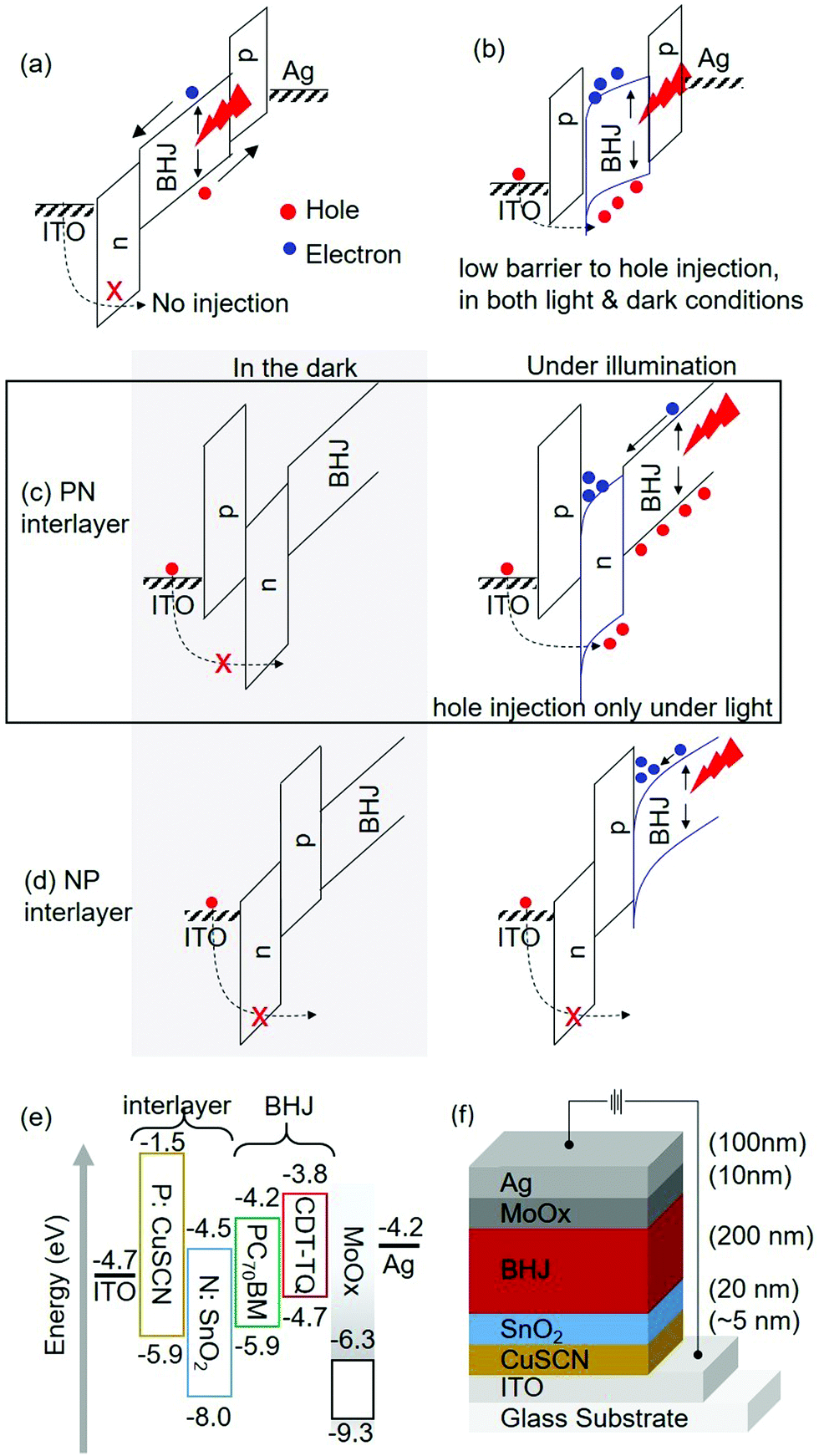 | ||
| Fig. 1 Interlayer designs. Energy diagrams of (a) a conventional photodiode with unipolar charge transporting interlayers and no photomultiplication and (b) a photodiode using a single charge blocking material, which induces photomultiplication but shows high noise current from charge injection in the dark. (c) Changing the interlayer over the ITO electrode to a pn heterojunction bilayer that enables photomultiplication and suppresses dark current. (d) Reversing the p- and n-type materials in the bilayer inhibits photomultiplication. (e) Energy levels of the materials used in this work. (f) Cross-sectional layers in our photomultiplication device. | ||
To decouple this trade-off between the background noise and the photocurrent, we introduce a bilayer heterojunction as the interlayer between the BHJ and the charge injecting electrode as shown in Fig. 1c. Instead of a single charge-transporting material, the interlayer consists of two materials with an energetic offset forming a pn junction. In the dark, hole injection is expected to be inhibited by the additional n-layer, suppressing the dark current in comparison to the configuration in Fig. 1b. Meanwhile, this bilayer can enable photomultiplication under illumination, because of photogenerated electrons that are trapped at the pn junction and consequently lower the hole injection barrier of the n-layer. We note that the order of the pn bilayer should be coordinated with respect to the applied bias. The configuration of Fig. 1c places the pn bilayer at forward bias for good charge injection under light. An alternative arrangement with the layers reversed in Fig. 1d would not trigger photomultiplication, since the trapped electrons will be too far from the n-layer and unable to effectively lower the injection barrier.
Based on the design strategy in Fig. 1c, this work presents organic SWIR detectors achieving excellent photomultiplicative gain with a dark current lower than conventional photodiodes without gain. After the photodiode performance is characterized in terms of detectivity and response speed, the SWIR sensor is integrated with an organic lightemitting diode to demonstrate an upconversion imager. Improvements in the upconversion efficiency are realized as a result of active photomultiplication in the sensor delivering more charges to the light emitter. This proof-of-concept demonstration shows that our new interlayer is widely applicable and compatible with different optical structures to boost the performance of organic SWIR devices.
Results and discussions
Effects of the heterojunction bilayer on photodiode performance
The materials and photodiode structure used in this work are shown in Fig. 1e. The interlayer next to ITO was a bilayer of hole-transporting copper thiocyanate25 (CuSCN) and electron-transporting tin oxide26–31 (SnO2). Other materials combination with similar energy levels to CuSCN and SnO2 are also applicable for the pn interlayer. During device operation, the indium tin oxide (ITO) electrode is under positive bias, and the pn interlayer is forward biased while the BHJ is reverse biased. Formulas for computing devices metrics are included in the Experimental section.Fig. 2a compares the current–voltage characteristics of photodiodes with a conventional interlayer (a single n-type SnO2, Fig. 1a) versus a pn bilayer (p: CuSCN/n: SnO2 stack, Fig. 1c and e). Under illumination at low applied biases <−1.3 V on the Ag electrode, the photocurrent was initially lower in the device with the bilayer than the conventional structure, because the additional CuSCN in the bilayer prevented the collection of photogenerated electrons. While trapped, the electrons bent the energy levels at the CuSCN/SnO2 interface and decreased the hole-injection barrier. As the applied bias was raised, hole injection increased, and eventually for a bias >−1.3 V the injected photocurrent through the bilayer stack exceeded the level measured in the conventional photodiode. The external quantum efficiency reached over 100% at −1.6 V, indicative of photomultiplication in the device with the bilayer.
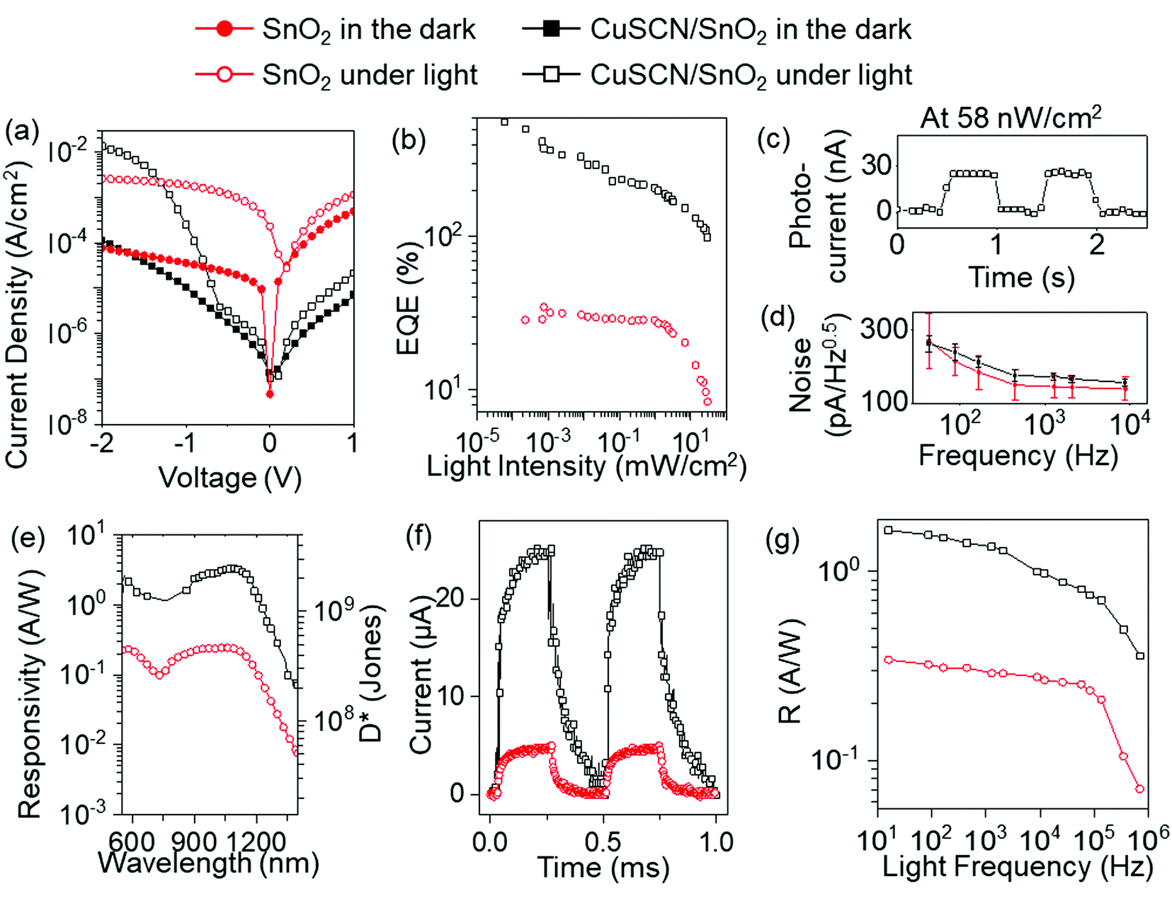 | ||
| Fig. 2 Comparison of the single and bilayer interlayers, with the devices biased at −1.5 V on the Ag electrode. (a) Current density versus applied voltage, measured in the dark and under 9.1 mW cm−2 illumination from a 1050 nm LED. (b) External quantum efficiency taken at the wavelength of 1050 nm as a function of incident light intensity. (c) Temporal photoresponse under 58 nW cm−2, with the 1050 nm LED modulated at 1 Hz. (d) Noise current as a function of measurement frequency. (e) Responsivity and specific detectivity measured at 313 Hz as a function of spectral wavelength, under 1.6 μW cm−2 illumination. (f) Temporal photoresponse under 0.15 mW cm−2, with the 1050 nm LED modulated at 2077 Hz. (g) Photoresponse amplitude versus the modulation frequency of the incident light at an intensity of 0.15 mW cm−2 from the 1050 nm LED. | ||
Meanwhile, the characteristics in the dark show a reduction in the dark current due to the bilayer, when compared to the conventional structure. The dark current in Fig. 2a is higher than devices operating in the visible but comparable to other infrared devices responsive to SWIR wavelengths longer than 1 μm.11 The reason for the high dark current in SWIR photodiodes is that the bandgap of the BHJ must be reduced in order to respond to longer wavelengths. Below −1.8 V, the bilayer enabled a dark current lower than the conventional structure in Fig. 1a. Since the energy difference between ITO and SnO2 is up to 3.3 eV, we thought the single SnO2 layer in the conventional structure would already be effective at blocking hole injection in the dark. However, adding a thin 5 nm CuSCN layer to the interlayer further reduced the dark current, and we attribute this effect to the elimination of pinhole leakage paths in the bilayer stack. For a bias voltage larger than −1.8 V, the dark current of the device with the bilayer increased faster than the single layer, because the applied electric field was raised to a point that the probability of charge injection from ITO into the n-SnO2 layer increased.32 Nonetheless, the rise in dark current was still negligible compared to the photomultiplication current. In the future, the n-type SnO2 can be changed to a material with an energy level closer to the BHJ at the lowest unoccupied molecular orbital (LUMO) to further reduce charge injection at high electric field. With the structure in this paper, for the voltage window between −1 V and −1.8 V, the device with the bilayer showed higher photocurrent while maintaining lower dark current than the device with the single SnO2 layer.
The device external quantum efficiency (EQE) as a function of incident light intensity is shown in Fig. 2b. The EQE of the conventional device was constant at ∼30% and independent of light intensity until it reached saturation around 1 mW cm−2. In contrast, the device with the CuSCN/SnO2 interlayer exhibited EQE's higher than 100% for light intensities below 10 mW cm−2. At 58 nW cm−2, the EQE was 560%. The EQE increased with decreasing intensities, and this trend is characteristic of a trap-assisted gain mechanism that has been observed in a variety of materials from organics to oxides to two-dimensional semiconductors.33–36 The photomultiplicative gain factor is proportional to τtrap/τtransit; when the charge transit time τtransit is shorter than the trap lifetime τtrap, the photocurrent is amplified by the gain factor. The lifetime of trapped charges was extended at low light intensity,33 because photogenerated charges occupied the deep trap states first before filling up shallow trap states. Charges trapped in deep states escaped more slowly than those in shallow states and thus led to a longer trap lifetime and increasing gain factor and EQE at low light intensity.
With a higher EQE enabled by photomultiplication, the detection limit of the device with CuSCN/SnO2 was extended to a lower light intensity than the conventional structure. The current of the device with CuSCN/SnO2 in Fig. 2c shows a clear photoresponse under modulated illumination at a low intensity of 58 nW cm−2, for which the conventional device did not show a clear signal above its background noise. The measured noise of the conventional device and the one with CuSCN/SnO2 are comparable at −1.5 V bias as seen in Fig. 2d. In Fig. 2e, we determined the detectivity versus incident wavelength for the devices measured at a frequency of 313 Hz and with a bias of −1.5 V. At the peak of 1100 nm, the detectivity D* reached 3.5 × 10⁹ Jones for the device with CuSCN/SnO2 and 6 × 10⁸ Jones for the conventional device, under the light intensity of 58 nW cm−2. From the detectivity values, we calculated the noise-equivalent power (NEP), which was 1.5 nW for the device with CuSCN/SnO2 and 8.9 nW for the conventional device.
Fig. 2f shows the temporal response of the devices when the incident light was modulated at 2 kHz. The device with CuSCN/SnO2 underwent photomultiplication, which caused a slower rise and fall time than the conventional device, since the charge injection and de-trapping processes would prolong the response time for the device to reach steady state. The frequency response of the devices is compared in Fig. 2g, in which the signal amplitudes dropped to −3 dB at 30 kHz for the device with CuSCN/SnO2 and 100 kHz for the conventional device. The gain-bandwidth product is 2.6 × 10⁵ Hz A W−1 for the devices, and the trade-off in speed with gain is typical for photomultiplication devices.
Integration of the bilayer heterojunction to improve upconversion imagers
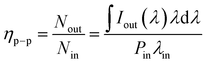
Following successful improvements on individual photodiodes, we extended the heterojunction bilayer design to enhance SWIR upconversion imagers for demonstrating the generalizability of this new interlayer in different applications. Upconversion imagers37–41 locally convert low-energy infrared photons absorbed by the photodetector layer into high-energy visible photons in the light emitter layer, thus serving as a compact visualization tool for infrared radiation. However, the photon-to-photon efficiency (ηp–p) of upconversion imagers is still limited42 and hinders the production of high-quality images. Applying photomultiplication in the upconversion process would increase charge injection into the emitter and raise its luminance, but this approach has only been demonstrated only for the near-infrared range or with quantum dots. Below we show the feasibility of applying our heterojunction bilayer to induce photomultiplication in SWIR ranges and increase the efficiency of organic upconversion imagers.Fig. 3a shows the schematic of our organic upconversion imager, which is an integrated structure of a photodiode (PD) and a light-emitting diode (LED) arranged as back-to-back diodes. We compare the effect of changing the PD interlayer on the upconverted light output in Fig. 3b. In the dark, the luminance was reduced for the device with the CuSCN/SnO2 interlayer, which was helpful for improving the imager contrast between regions of active upconversion and background emission. Under an illumination of 5 mW cm−2 at 1050 nm, as the applied bias was increased, the device with CuSCN/SnO2 leveraged photomultiplication to increase charge injection into the emitter, and its luminance surpassed the conventional structure with only SnO2 for biases over 4.4 V. In Fig. 3c, the device current densities corresponding to the luminance outputs show that there was 2 times higher current running through the photomultiplication device than the conventional device at 8 V. As a result, the ηp–p efficiency of the imager was doubled from 0.2% to 0.4% by changing the PD interlayer from only SnO2 to the bilayer CuSCN/SnO2.
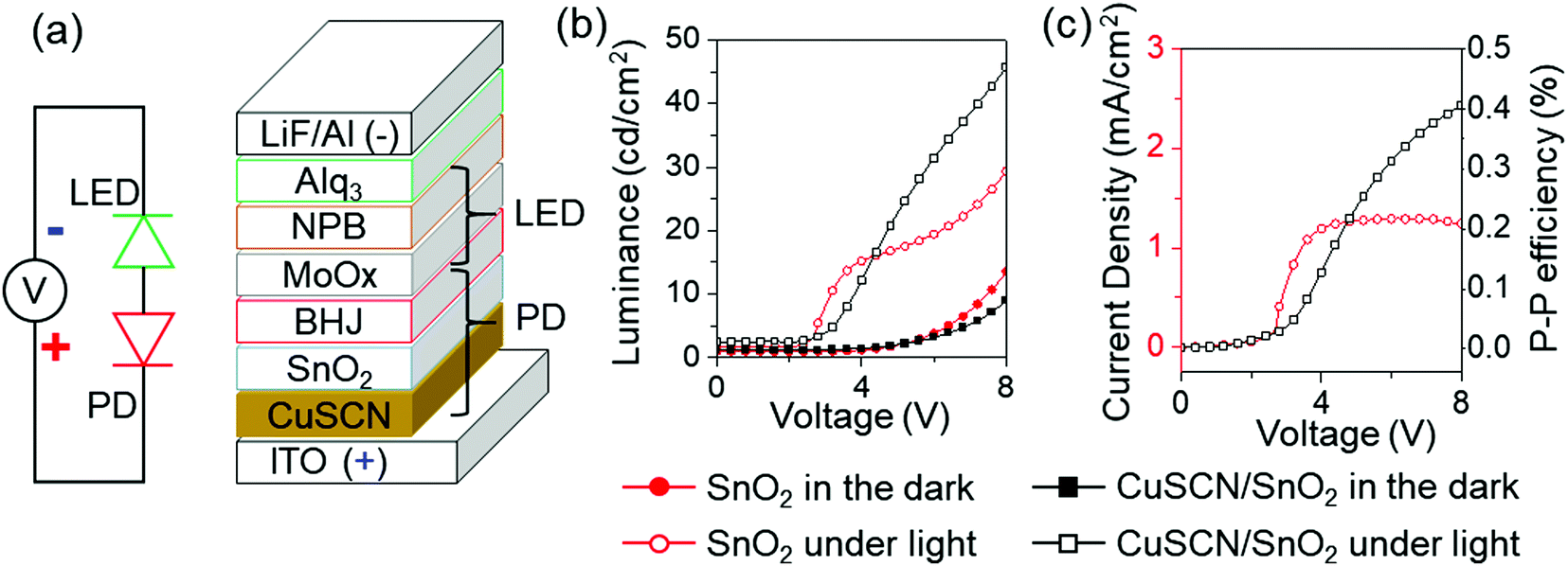 | ||
| Fig. 3 Upconversion imagers with different interlayers in the photodiode stack. The incident light was at an intensity of 5 mW cm−2 from a 1050 nm light source. (a) Schematics of the upconversion imager with the CuSCN/SnO2 bilayer. (b) Luminance of the visible light emitted from the imager versus the applied bias. (c) Current density and photon-to-photon upconversion efficiency versus the applied bias. | ||
To compare the quality of upconversion images, the two imagers with different interlayers were used to visualize stress gradients in a sample placed between polarization filters as shown in Fig. 4a. The sample was a plastic protractor, and for plastics made by injection molding, there would usually be stress gradients prominent at corners and edges due to different materials flow rate in the fabrication process. Local stress variations would be shown as bright and dark regions depending on whether the refracted light from the sample aligned with the polarization filter in front of the imager. In Fig. 4b and c, the sample image acquired with the imager using CuSCN/SnO2 shows better contrast than that with only SnO2 as the interlayer. Using the image analysis software ImageJ under the RGB stack function, the contrast between the peak light level to the background is 3.9 for the former photomultiplication device and 2.3 for the latter, indicating improved quality through the interlayer modification. While the histograms in Fig. 4d are limited to 256 levels due to the image conversion process, the contrast increased by 1.7 times.
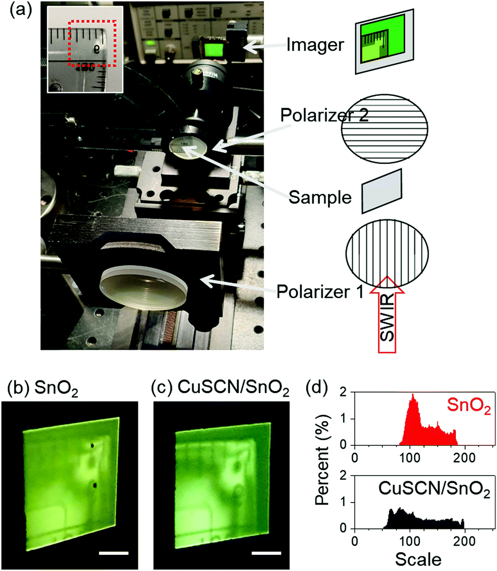 | ||
| Fig. 4 Results of upconversion images. (a) Imaging setup. The red box on the plastic protractor indicates the area being imaged. Upconversion images produced by (b) the imager with conventional interlayer and (d) the imager with the heterojunction interlayer. The scale bar represents 5 mm. The imagers were operated at 5 V, and the sample was under 290 μW cm−2 illumination from a 940 nm LED. (d) Histograms of images in parts (b) and (c). | ||
Conclusion
This work has demonstrated the performance of a bilayer heterojunction CuSCN/SnO2 as the charge transporting interlayer in organic SWIR photodetectors to realize photomultiplication and low dark current, with an EQE up to 560% and a detectivity of 3.5 × 10⁹ Jones. As the bilayer was applied to upconversion imagers, the upconversion efficiency and imager contrast nearly doubled when compared to the conventional structure. The bilayer heterojunction design can be further optimized; for example, the thickness of the SnO2 layer is currently set at 20 nm to be the same in the control and the new bilayer, but it is possible that this layer thickness can be slightly reduced in the bilayer without impacting the dark current. A thinner bilayer can increase charge injection during the photomultiplication process to reach for higher amplification. Modifying the interlayer to enhance photomultiplication offers a key advantage that it is adaptable to different BHJ choices, making it versatile and compatible with future semiconductor materials that can extend the spectral range and functionalities of organic infrared detectors.Experimental procedures
Materials
The synthesis of the polymer (poly(4-(5-(4-(3,5-bis(dodecyloxy)benzylidene)-4H-cyclopenta[2,1-b:3,4-b′]dithiophen-2-yl)thiophen-2-yl)-6,7-dioctyl-9-(thiophen-2-yl)-[1,2,5]thiadiazolo[3,4-g]quinoxaline)) (CDT-TQ) was described in ref. 43 and the polymer belonged to a class of narrow bandgap donor–acceptor copolymers.44 The acceptor [6,6]-phenyl-C71-butyric acid methyl ester (PC70BM) was purchased from Ossila Ltd. Camphoric acid anhydride (CA), which is used to increase the dielectric constant of the BHJ layer to enhance exciton dissociation,43 was purchased from Sigma-Aldrich Ltd. The CDT-TQ, PC70BM, and CA were blended at 2:4:1 weight ratio dissolved in 1,2-dichlorobenzene at a concentration of 28 mg mL−1. An additive 1,8-diiodooctane was added to the blend at a volume ratio of 3%. This BHJ blend solution was stirred at 70 °C for at least 24 hours. The solution for the CuSCN layer was prepared by dissolving CuSCN in diethyl sulfide at a concentration of 2 mg mL−1. We have varied the concentration of the CuSCN solution from 1.5 to 2 mg mL−1. It is found that 2 mg mL−1 is the lowest concentration for CuSCN processing. If the solution concentration is lower than 2 mg mL−1, the sample showed non-uniform coverage of the film. The solution for electron-transporting SnO2 was prepared by dissolving SnCl2·H2O in ethanol at concentration of 0.07 M, and the solution45 was stirred in a water bath at 80 °C for 4 hours followed by 40 °C for another 4 hours.
Photodiode fabrication
The ITO substrates with a sheet resistance ∼15 Ω sq−1 were cleaned by detergent, deionized water, acetone, and isopropanol, submerged in each solvent for 15 min sonication. For device having SnO2 single layer, the SnO2 layer was prepared by spin-coating the precursor solution at 3000 rpm for 40 s. The sample was annealed at 180 °C for 1 hour, resulting in a thin film of ∼20 nm. For device having CuSCN/SnO2 bilayer, the CuSCN layer was prepared by spin-coating the solution at 1200 rpm for 40 s and then annealing at 90 °C for 5 min in the ambient, resulting in a thin film of ∼5 nm. The SnO2 layer was prepared by spin-coating the precursor solution at 3000 rpm for 40 s and annealing up to 170 °C for 1 hour. The substrates with interlayers were transferred to a nitrogen-filled glovebox to deposit the BHJ layer. The BHJ blend solution was spin-coated at 2000 rpm for 40 s on top of the SnO2 layer to form a film with a thickness of ∼200 nm. Afterwards, 10 nm molybdenum oxide (MoOx) and 100 nm Ag layer were thermally deposited through a shadow mask, defining an active area of 0.09 cm2. All the devices were encapsulated before characterization in the ambient.Photodiode characterization
In the current–voltage measurements, the bias voltage was applied by a sourcemeter (Keithley 2400), and the current was recorded by the same sourcemeter. SWIR light was from a LED (Thorlabs, LED1050L) with a peak wavelength of 1050 nm. The light intensity was controlled by adjusting the distance between device and LED and measured by a germanium (Ge) detector (Newport, 818IR). In the EQE measurements, the monochromatic light source was modulated at 313 Hz by an optical chopper. The device photocurrent was amplified through a pre-amplifier (Stanford Research Systems, SRS 570) and then recorded by a lock-in amplifier (Stanford Research Systems, SR 530). The noise spectral densities were measured using the pre-amplifier connected to the lock-in amplifier. The reference frequency in the noise current measurements was controlled by a function generator (Rigol, DG 2401A) serving as the external trigger for the lock-in amplifier. The device noise was calculated by subtracting the equipment background noise. Transient photocurrent was measured under the 1050 nm LED light modulated by the function generator, and the corresponding photocurrent was recorded by an oscilloscope (Rigol, DS1054).The external quantum efficiency was calculated from the photocurrent:
| EQE = (Jph/Pillumin)(hc/λq) = R(hc/λq) | (1) |
The specific detectivity was determined by
| D* = RA0.5/Sn, | (2) |
The noise equivalent power is wavelength dependent and related to detectivity by
 | (3) |
Upconversion imager fabrication and characterization
For the upconversion imager, additional layers were deposited on top of the PD layers following the schematic in Fig. 3a. The films of 35 nm N,N′-Bis(naphthalen-1-yl)-N,N′-bis(phenyl)benzidine (NPB), 50 nm tris(8-hydroxyquinoline)aluminum(III) (Alq3), 2 nm lithium fluoride (LiF), and 300 nm Al layers were sequentially deposited on the MoOx layer by thermal evaporation.The intensity of visible light emission from the upconversion device was measured by a Si detector (Thorlabs DET36A). SWIR light was shine onto the upconversion imager at an incident angle of 45°. A shortpass filter (<800 nm) was placed before the Si detector to block surface-reflected SWIR light that could add unwanted contribution to the visible light measurement. The spectrum of the emitted visible light was measured by a spectrometer (Ocean Optics USB2000).
The upconversion efficiency for converting SWIR photons to visible photons is known as the photon-to-photon conversion efficiency and obtained by37
 | (4) |
Author contributions
C. S. and N. L., and T. N. N. designed the experiments and analyzed the data. C. S. and B. S. conducted the fabrication and measurement of the devices. N. E. synthesized the SWIR polymer under the supervision of J. D. A. The principal investigator T. N. N. conceived the interlayer concept and supervised the project. All authors contributed to discussions and writing of the manuscript.Data availability statement
The data that support the findings of this study are available from the corresponding author upon reasonable request.Conflicts of interest
The authors declare no conflict of interest.Acknowledgements
The author T. N. N. is grateful for the support from National Science Foundation award MCA-2120701. J. D. Azoulay was supported by the Air Force Office of Scientific Research under the Organic Materials Chemistry Program (FA9550-17-1-0261) and was supported by the National Science Foundation (OIA-1757220).References
- A. Rogalski, Infrared and Terahertz Detectors, CRC Press, Third edn, 2019 Search PubMed.
- R. H. Wilson, K. P. Nadeau, F. B. Jaworski, B. J. Tromberg and A. J. Durkin, Review of Short-Wave Infrared Spectroscopy and Imaging Methods for Biological Tissue Characterization, J. Biomed. Opt., 2015, 20(3), 030901 CrossRef PubMed.
- Q. Li, Y. Guo and Y. Liu, Exploration of Near-Infrared Organic Photodetectors, Chem. Mater., 2019, 31(17), 6359–6379 CrossRef CAS.
- Z. Ge, N. Xu, Y. Zhu, K. Zhao, Y. Ma, G. Li and Y. Chen, Visible to Mid-Infrared Photodetection Based on Flexible 3D Graphene/Organic Hybrid Photodetector with Ultrahigh Responsivity at Ambient Conditions, ACS Photonics, 2022, 9(1), 59–67 CrossRef CAS.
- N. Li, P. Mahalingam, J. H. Vella, D.-S. S. Leem, J. D. Azoulay and T. N. Ng, Solution-Processable Infrared Photodetectors: Materials, Device Physics, and Applications, Mater. Sci. Eng., R, 2021, 146, 100643 CrossRef.
- N. Li, N. Eedugurala, J. D. Azoulay and T. N. Ng, A Filterless Organic Photodetector Electrically Switchable between Visible and Infrared Detection, Cell Rep. Phys. Sci., 2022, 3(1), 100711 CrossRef CAS.
- N. Strobel, M. Seiberlich, T. Rodlmeier, U. Lemmer and G. Hernandez-Sosa, Non-Fullerene-Based Printed Organic Photodiode with High Responsivity and Megahertz Detection Speed, ACS Appl. Mater. Interfaces, 2018, 10(49), 42733 CrossRef CAS PubMed.
- J. Miao and F. Zhang, Recent Progress on Photomultiplication Type Organic Photodetectors, Laser Photonics Rev., 2019, 13(2), 1800204 Search PubMed.
- G. Simone, M. J. Dyson, S. C.-J. J. Meskers, R. A.-J. J. Janssen and G. H. Gelinck, Organic Photodetectors and Their Application in Large Area and Flexible Image Sensors: The Role of Dark Current, Adv. Funct. Mater., 2020, 30(20), 1904205 CrossRef CAS.
- Z. Wu, N. Li, N. Eedugurala, J. D. Azoulay, D.-S. Leem and T. N. Ng, Noise and Detectivity Limits in Organic Shortwave Infrared Photodiodes with Low Disorder, npj Flexible Electron., 2020, 4(1), 6 CrossRef.
- S. Gielen, C. Kaiser, F. Verstraeten, J. Kublitski, J. Benduhn, D. Spoltore, P. Verstappen, W. Maes, P. Meredith, A. Armin and K. Vandewal, Intrinsic Detectivity Limits of Organic Near-Infrared Photodetectors, Adv. Mater., 2020, 32(47), 2003818 CrossRef CAS PubMed.
- J. Kublitski, A. Hofacker, B. K. Boroujeni, J. Benduhn, V. C. Nikolis, C. Kaiser, D. Spoltore, H. Kleemann, A. Fischer, F. Ellinger, K. Vandewal and K. Leo, Reverse Dark Current in Organic Photodetectors and the Major Role of Traps as Source of Noise, Nat. Commun., 2021, 12(1), 551 CrossRef CAS PubMed.
- Y. Fang, A. Armin, P. Meredith and J. Huang, Accurate Characterization of Next-Generation Thin-Film Photodetectors, Nat. Photonics, 2019, 13(1), 1–4 CrossRef CAS.
- Y. Wu, K. Fukuda, T. Yokota and T. Someya, A Highly Responsive Organic Image Sensor Based on a Two-Terminal Organic Photodetector with Photomultiplication, Adv. Mater., 2019, 31(43), 1903687 CrossRef CAS PubMed.
- S. Yoon, G. S. Lee, K. M. Sim, M. J. Kim, Y. H. Kim and D. S. Chung, End-Group Functionalization of Non-Fullerene Acceptors for High External Quantum Efficiency over 150 000% in Photomultiplication Type Organic Photodetectors, Adv. Funct. Mater., 2021, 31(1), 2006448 CrossRef CAS.
- S. Xing, J. Kublitski, C. Hänisch, L. C. Winkler and T. Li, yi; Kleemann, H.; Benduhn, J.; Leo, K. Photomultiplication-Type Organic Photodetectors for Near-Infrared Sensing with High and Bias-Independent Specific Detectivity, Adv. Sci., 2022, 9(7), 2105113 CrossRef CAS PubMed.
- J. Kim, M. Kang, S. Lee, C. So and D. S. Chung, Interfacial Electrostatic-Interaction-Enhanced Photomultiplication for Ultrahigh External Quantum Efficiency of Organic Photodiodes, Adv. Mater., 2021, 33(52), 2104689 CrossRef CAS PubMed.
- Z. Wu, W. Yao, A. E. London, J. D. Azoulay and T. N. Ng, Elucidating the Detectivity Limits in Shortwave Infrared Organic Photodiodes, Adv. Funct. Mater., 2018, 28(18), 1800391 CrossRef.
- I. Constantinou, X. Yi, N. T. Shewmon, E. D. Klump, C. Peng, S. Garakyaraghi, C. K. Lo, J. R. Reynolds, F. N. Castellano and F. So, Effect of Polymer-Fullerene Interaction on the Dielectric Properties of the Blend, Adv. Energy Mater., 2017, 7(13), 1601947 CrossRef.
- J. Benduhn, K. Tvingstedt, F. Piersimoni, S. Ullbrich, Y. Fan, M. Tropiano, K. A. McGarry, O. Zeika, M. K. Riede, C. J. Douglas, S. Barlow, S. R. Marder, D. Neher, D. Spoltore and K. Vandewal, Intrinsic Non-Radiative Voltage Losses in Fullerene-Based Organic Solar Cells, Nat. Energy, 2017, 2(6), 17053 CrossRef CAS.
- K. Yang, J. Wang, Z. Zhao, Y. Sun, M. Liu, Z. Zhou, X. Zhang and F. Zhang, Highly Sensitive Photomultiplication Type Polymer Photodetectors by Manipulating Interfacial Trapped Electron Density, Chem. Eng. J., 2022, 435(P2), 134973 CrossRef CAS.
- D. Guo, D. Yang, J. Zhao, A. Vadim and D. Ma, Role of Interfaces in Controlling Charge Accumulation and Injection in the Photodetection Performance of Photomultiplication-Type Organic Photodetectors, J. Mater. Chem. C, 2020, 8(26), 9024–9031 RSC.
- N. Li, J. Lim, J. D. Azoulay and T. N. Ng, Tuning the Charge Blocking Layer to Enhance Photomultiplication in Organic Shortwave Infrared Photodetectors, J. Mater. Chem. C, 2020, 8(43), 15142–15149 RSC.
- Z. Zhao, J. Wang, C. Xu, K. Yang, F. Zhao, K. Wang, X. Zhang and F. Zhang, Photomultiplication Type Broad Response Organic Photodetectors with One Absorber Layer and One Multiplication Layer, J. Phys. Chem. Lett., 2020, 11(2), 366–373 CrossRef CAS PubMed.
- N. Yaacobi-Gross, N. D. Treat, P. Pattanasattayavong, H. Faber, A. K. Perumal, N. Stingelin, D. D.-C. Bradley, P. N. Stavrinou, M. Heeney and T. D. Anthopoulos, High-Efficiency Organic Photovoltaic Cells Based on the Solution-Processable Hole Transporting Interlayer Copper Thiocyanate (CuSCN) as a Replacement for PEDOT:PSS, Adv. Energy Mater., 2015, 5(3), 1401529 CrossRef.
- J. Huang, J. Lee, H. Nakayama, M. Schrock, D. X. Cao, K. Cho, G. C. Bazan and T. Q. Nguyen, Understanding and Countering Illumination-Sensitive Dark Current: Toward Organic Photodetectors with Reliable High Detectivity, ACS Nano, 2021, 15(1), 1753–1763 CrossRef CAS PubMed.
- J. Liang, Z. Chen, G. Yang, H. Wang, F. Ye, C. Tao and G. Fang, Achieving High Open-Circuit Voltage on Planar Perovskite Solar Cells via Chlorine-Doped Tin Oxide Electron Transport Layers, ACS Appl. Mater. Interfaces, 2019, 11(26), 23152–23159 CrossRef CAS PubMed.
- Y. Jiang, L. Sun, F. Jiang, C. Xie, L. Hu, X. Dong, F. Qin, T. Liu, L. Hu, X. Jiang and Y. Zhou, Photocatalytic Effect of ZnO on the Stability of Nonfullerene Acceptors and Its Mitigation by SnO2 for Nonfullerene Organic Solar Cells, Mater. Horiz., 2019, 6(7), 1438–1443 RSC.
- M. F. Mohamad Noh, C. H. Teh, R. Daik, E. L. Lim, C. C. Yap, M. A. Ibrahim, N. Ahmad Ludin, A. R.-B. Mohd Yusoff, J. Jang and M. A. Mat Teridi, The Architecture of the Electron Transport Layer for a Perovskite Solar Cell, J. Mater. Chem. C, 2018, 6(4), 682–712 RSC.
- L. Xiong, Y. Guo, J. Wen, H. Liu, G. Yang, P. Qin and G. Fang, Review on the Application of SnO2 in Perovskite Solar Cells, Adv. Funct. Mater., 2018, 28(35), 1802757 CrossRef.
- Q. Jiang, X. Zhang and J. You, SnO2: A Wonderful Electron Transport Layer for Perovskite Solar Cells, Small, 2018, 14(31), 1801154 CrossRef PubMed.
- C. Xiong, R. H. Yao, W. J. Wan and J. X. Xu, Fabrication and Electrical Characterization of ZnO Rod Arrays/CuSCN Heterojunctions, Optik, 2014, 125(2), 785–788 CrossRef CAS.
- H. Kim, Z. Wu, N. Eedugurala, J. D. Azoulay and T. N. Ng, Solution-Processed Phototransistors Combining Organic Absorber and Charge Transporting Oxide for Visible to Infrared Light Detection, ACS Appl. Mater. Interfaces, 2019, 11(40), 36880–36885 CrossRef CAS PubMed.
- Y. S. Rim, K. C. Ok, Y. M. Yang, H. Chen, S. H. Bae, C. Wang, Y. Huang, J. S. Park and Y. Yang, Boosting Responsivity of Organic-Metal Oxynitride Hybrid Heterointerface Phototransistor, ACS Appl. Mater. Interfaces, 2016, 8(23), 14665–14670 CrossRef CAS PubMed.
- M. M. Furchi, D. K. Polyushkin, A. Pospischil and T. Mueller, Mechanisms of Photoconductivity in Atomically Thin MoS2, Nano Lett., 2014, 14(11), 6165–6170 CrossRef CAS PubMed.
- A. Pierre, A. Gaikwad and A. C. Arias, Charge-Integrating Organic Heterojunction Phototransistors for Wide-Dynamic-Range Image Sensors, Nat. Photonics, 2017, 11(3), 193–199 CrossRef CAS.
- R. Hany, M. Cremona and K. Strassel, Recent Advances with Optical Upconverters Made from All-Organic and Hybrid Materials, Sci. Technol. Adv. Mater., 2019, 20(1), 497–510 CrossRef PubMed.
- Q. Song, T. Lin, Z. Su, B. Chu, H. Yang, W. Li and C. S. Lee, Organic Upconversion Display with an over 100% Photon-to-Photon Upconversion Efficiency and a Simple Pixelless Device Structure, J. Phys. Chem. Lett., 2018, 9(23), 6818–6824 CrossRef CAS PubMed.
- N. Li, N. Eedugurala, D. S. Leem, J. D. Azoulay and T. N. Ng, Organic Upconversion Imager with Dual Electronic and Optical Readouts for Shortwave Infrared Light Detection, Adv. Funct. Mater., 2021, 31(16), 2100565 CrossRef CAS.
- D. Yang, X. Zhou, D. Ma, A. Vadim, T. Ahamad and S. M. Alshehri, Near Infrared to Visible Light Organic Up-Conversion Devices with Photon-to-Photon Conversion Efficiency Approaching 30%, Mater. Horiz., 2018, 5(5), 874–882 RSC.
- H. Ren, J.-D. Chen, Y.-Q. Li and J.-X. Tang, Recent Progress in Organic Photodetectors and Their Applications, Adv. Sci., 2021, 8(1), 2002418 CrossRef CAS PubMed.
- W. Zhou, Y. Shang, F. P. García de Arquer, K. Xu, R. Wang, S. Luo, X. Xiao, X. Zhou, R. Huang, E. H. Sargent, Z. Ning, F. P.-G. D. Arquer, K. Xu, R. Wang, S. Luo, X. Xiao, X. Zhou, R. Huang, E. H. Sargent and Z. Ning, Solution-Processed Upconversion Photodetectors Based on Quantum Dots, Nat. Electron., 2020, 3(5), 251–258 CrossRef CAS.
- Z. Wu, Y. Zhai, W. Yao, N. Eedugurala, S. Zhang, L. Huang, X. Gu, J. D. Azoulay and T. N. Ng, The Role of Dielectric Screening in Organic Shortwave Infrared Photodiodes for Spectroscopic Image Sensing, Adv. Funct. Mater., 2018, 28(50), 1805738 CrossRef.
- J. H. Vella, L. Huang, N. Eedugurala, K. Mayer, T. N. Ng and J. Azoulay, Broadband Infrared Photodetection Using a Narrow Bandgap Conjugated Polymer, Sci. Adv., 2021, 7(24), abg2418 CrossRef PubMed.
- V. H. Tran, R. Khan, I. H. Lee and S. H. Lee, Low-Temperature Solution-Processed Ionic Liquid Modified SnO2 as an Excellent Electron Transport Layer for Inverted Organic Solar Cells, Sol. Energy Mater. Sol. Cells, 2018, 179(1), 260–269 CrossRef CAS.
| This journal is © The Royal Society of Chemistry 2022 |