
 Open Access Article
 This Open Access Article is licensed under a Creative Commons Attribution-Non Commercial 3.0 Unported Licence
Study on the electronic and optical properties of van der Waals heterostructures of blue phosphorene and Janus-WSeS monolayers for photocatalytic water splitting
Shiquan
Feng
 ab,
Feng
Guo
c,
Chaosheng
Yuan
ab,
Zheng
Wang
ab,
Feng
Miao
*d and
Huanjun
Zhang
*ab
ab,
Feng
Guo
c,
Chaosheng
Yuan
ab,
Zheng
Wang
ab,
Feng
Miao
*d and
Huanjun
Zhang
*ab
aHenan Key Laboratory of Magnetoelectronic Information Functional Materials, Zhengzhou University of Light Industry, Zhengzhou, 450002, China. E-mail: 2010067@zzuli.edu.cn
bSchool of Physics and Electronic Engineering, Zhengzhou University of Light Industry, Zhengzhou, Henan 450002, China
cSchool of Physical Science and Information Technology, Liaocheng University, Liaocheng, 252000, China
dKey Laboratory of State Ethnic Affairs Commission for Electronic and Information Engineering, Southwest Minzu University, Chengdu, 610041, China. E-mail: miaofeng-007@163.com
First published on 11th November 2022
Abstract
In this paper, we designed a series of heterostructures by assembling the blue phosphorene and Janus-WSeS monolayers together and then selected a stable blue-P/Janus-WSeS van der Waals heterostructure with type-II band arrangement. Further exploration of the band edge shows that it is fit to be the photocatalyst for water splitting. The results from tuning optoelectronic properties via biaxial strain show that the strain is an effective method to adjust the size of the band gap and the band alignment. According to the requirements, a suitable strain can be chosen to adjust the band of the heterostructure. In addition, the absorption coefficient shows a considerable value in the UV region, and the negative strain will enhance the absorption of UV light and weaken the absorption of visible light. Due to the favorable band edge positions and strong absorption in UV light, the blue-P/WSeS heterostructure can be considered as a potential visible and UV light irradiation catalyst for water splitting, and the catalytic activity can be adjusted by strain.
1. Introduction
Since 2004 when K. S. Novoselov et al. obtained single-layer graphene graphite,1 a large number of new 2D materials have emerged.2–7 Among them, two-dimensional (2D) phosphorus has been widely investigated, and four allotropes have been found. They are black phosphorus, blue phosphorus (blue-P), γ-phosphorus, and δ-phosphorus.8 The successful preparation of stable blue-P at room temperature by the epitaxial growth method quickly attracted people's attention5 because it has similar lattice parameters to TMDs, such as MoX2 and WX2 (X = S, Se). Both 2D phosphorene and transition metal dichalcogenides (TMDs) MX2 (M = Mo, W, Nb and V; X = S, Se, and Te) have been widely studied in recent decades due to their excellent physical and chemical properties.9–14 But single two-dimensional structures usually have some shortcomings. For example, the zero band gap of graphene limits its application in optoelectronic devices;15 the high recombination rate of photo-generated carriers of ultrathin CdS nanosheets greatly influences its performance in photocatalytic fields.16 Assembling van der Waals (vdW) heterostructures by different 2D monolayers is an effective method to improve their performances. Not only can heterostructures maintain the advantages of single 2D structures, but they also make up for their disadvantages in electronic and optical properties.17–21 Thus, heterostructures have attracted the attention of scientists and scholars in recent years. For example, Shahid et al.22 designed a boron phosphide-blue phosphorene vdW heterostructure by boron phosphide and blue phosphorene monolayers, and further studies show that this heterostructure is a potential candidate for water splitting at low pH values. In addition, the same research group23 also reported several Mo(W)Te2-As vdW heterostructures as promising photocatalysts for overall water splitting.Due to their similar lattice parameters, vdW heterostructures can be formed by assembling 2D phosphorene and TMDs monolayers together. Sharma et al.24 studied the properties of the blue-P/MoS2 heterostructure, and the results show that using this heterostructure as an interacting layer with the analyte can greatly enhance the sensitivity of the surface plasmon resonance sensor. Then, investigation by Bian et al.25 showed that blue-P/MoS2 vdW heterostructure with 3d transition metal absorption in the interlayer transitions from semiconductor to spin-polarized metals. Thus, it can be considered a candidate for nanoelectronics and spintronics device material. Huang et al.26 explored the strain effect on the electronic properties of blue-P/Janus-MoSeS and blue-P/Janus-MoSSe van der Waals heterostructure by first-principles studies, and the results show that strain engineering provides an effective avenue to tune the electronic properties of 2D vdW heterostructures. Using the density functional theory, Wang et al.27 studied the electronic and photocatalytic properties of WS2/blue-P and further sought the effect of uniaxial and biaxial strains on the performances of these heterostructures. The modulation of electronic structure and band offsets of blue-P/WSe2 vdW heterostructure via applied vertical compressive strain have also been investigated through first-principles calculations by Zhang et al.28
As sister materials of MX2 monolayers, Janus MSSe monolayers are formed by replacing the chalcogen anion layer with another dissimilar chalcogen layer.29,30 Because the symmetry of the out of plane mirror image is destroyed, they provide a new set of characteristics better than MX2 monolayers. Compared with the corresponding MX2, the Janus-MSSe can obtain more possible heterostructures by combining them with other 2D monolayer materials. Moreover, heterostructure stacking by Janus-MSSe and other 2D monolayers also shows excellent photoelectric properties.31,32 However, to date, few studies of vdW heterostructure stacking by blue-P and Janus-WSeS (or WSSe) monolayers have been reported. In this study, we systematically designed the possible vdW heterostructures, investigated their properties, and explored the effect of biaxial strain. Through this study, it is expected to find new possible water splitting catalysts.
2. Computational methods and details
In this work, we performed first-principles calculations using Vienna Ab initio Simulation Package (VASP) software with the Projection Augmented Wave (PAW) method33,34 to study the tuning of electronic properties of vdW heterostructure stacking by blue-P and Janus-WSeS (or WSSe) monolayers via biaxial strain. The conjugate gradient (CG) algorithm is chosen to optimize the heterostructures. In addition, the vdW interaction between layers plays an important role in determining the structural and electronic properties of the heterostructure, and hence Grimme's DFT-D3 method is adopted to consider this interaction.35,36 To obtain accurate band gaps for these 2D structures, the Heyd–Scuseria–Ernzerhof (HSE) method is employed to investigate their electronic properties.37 The Brillouin zone sampling was performed using a Monkhorst-pack grid to set k points.38 We used a 12 × 12 × 1 point grid to ensure calculation accuracy. The cut-off energy was set to 520 eV. For the structural optimization process, all the structures are optimized until the total energy is less than 10−6 eV per atom and the ionic Hellmann–Feynman force is less than 0.01 eV Å−1. A biaxial strain parallel to the stacking layers of vdW heterostructure ranging from −6% to 6% is applied to regulate its electronic and optical properties. To eliminate the interaction of interlayer caused by periodic boundary conditions, a 20 Å vacuum layer is added in the z-direction.The optical properties and absorption coefficient can be calculated from the complex dielectric function by the following relationship,
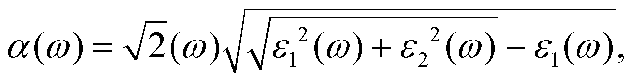 | (1) |
While the imaginary part of the complex dielectric function ε2(ω) can be expressed as the functional of the occupied and unoccupied states matrix elements with the following formula,
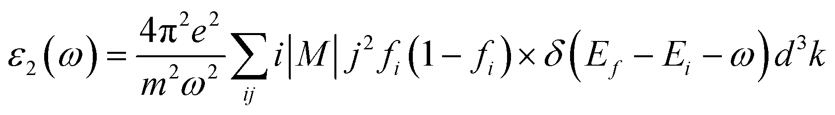 | (2) |
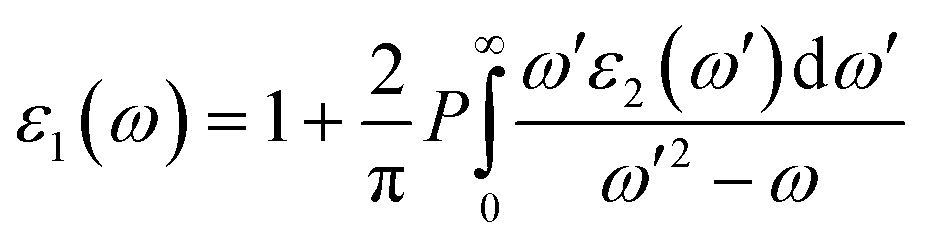 | (3) |
3 Results and discussion
3.1 Geometric structure and stability
Before investigating the blue-P/Janus-WSeS and blue-P/Janus-WSSe vdW heterostructure, we optimized the geometric structure of blue-P and Janus-WSeS (WSSe) monolayers. Our calculated lattice constant of the WSeS (WSSe) monolayer is 3.25 Å, which is between the lattice constants of WS2 (3.19 Å) and WSe2 (3.34 Å) from a previous report,41 and the calculated lattice constant of the blue-P monolayer is 3.28 Å, which is consistent with previous studies.42Due to the similar structure and lattice parameters, blue-P/Janus-WSeS and blue-P/WSSe vdW heterostructures can be constructed by the 1 × 1 primitive cells of blue-P and Janus-WSeS (WSSe) monolayers. As shown in Fig. 1, we presented four stacking configurations, AA, AB, AC, and AD stacking, for blue-P/Janus-WSeS vdW heterostructures. The structures for blue-P/Janus-WSSe vdW heterostructures are similar to blue-P/Janus-WSeS vdW heterostructures. The positions of Se and S atoms were swapped, so they are not presented here. Lattice mismatch can be calculated by the following formula,
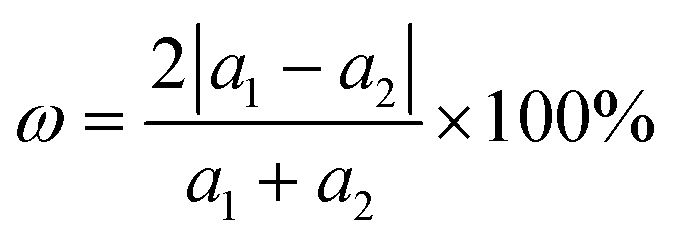 | (4) |
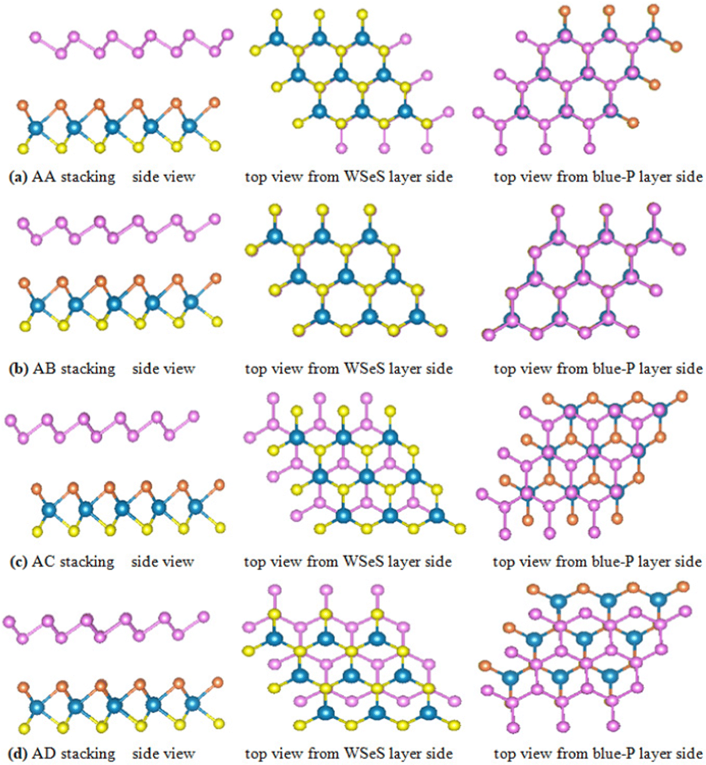 | ||
| Fig. 1 Top and side views of blue-P/Janus-WSeS vdW heterostructures with different stacking configurations: (a) AA stacking, (b) AB stacking, (c) AC stacking, (d) AD stacking. | ||
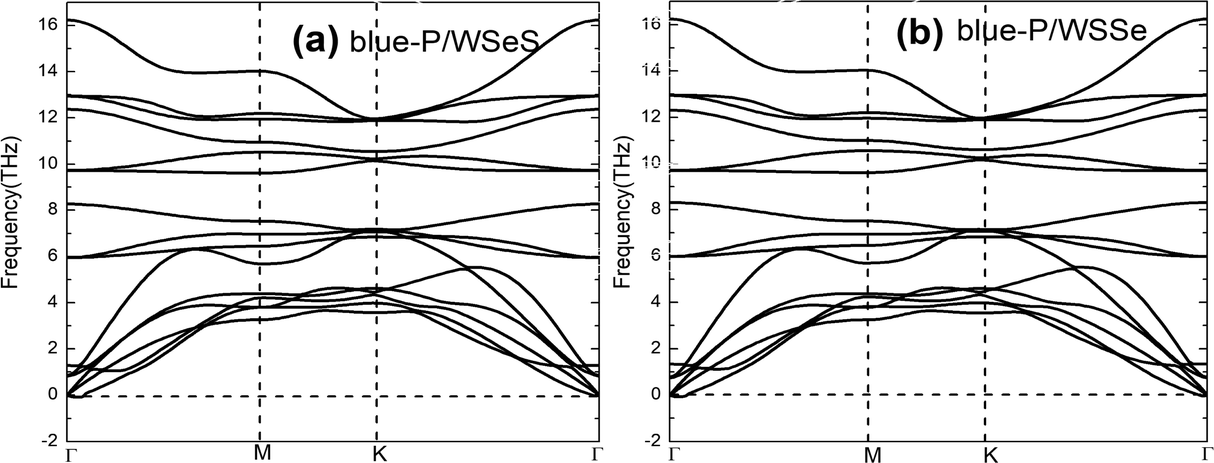
To explore the stability of these possible vdW heterostructures, their formation energies (Ef) are calculated. The formation energies Ef can be obtained by the formula Ef = Eheter − Elayer1 − Elayer2, where Eheter, Elayer1, and Elayer2 are the total energies of the heterostructures, blue-P monolayer, and Janus-WSeS (WSSe) monolayer, respectively. In Table 1, we present the optimized lattice parameter, formation energy, and layer distance of different configurations of the heterostructure stacking by blue-P and Janus-WSeS monolayers. Results show the AB stacking configuration is the most stable mode for both blue-P/Janus-WSeS and blue-P/Janus-WSSe vdW heterostructure from the perspective of energy, and their lowest formation energies are −0.901 and −0.893 eV per unit cell, respectively. To further verify the stability of the structures, we calculated their phonon dispersion curves. As shown in Fig. 2, the phonon spectra of AB stacking structures for blue-P/Janus-WSeS and blue-P/Janus-WSSe vdW heterostructure almost have no negative frequencies in the whole first Brillouin zone. This further indicates these configurations are dynamically stable. Therefore, in the following work, we only focus on the AB-stacked blue-P/Janus-WSeS and blue-P/Janus-WSSe vdW heterostructure and refer to them as blue-P/WSeS and blue-P/WSSe heterostructure for short, respectively. The equilibrium distances between the two monolayers for blue-P/Janus-WSeS and blue-P/Janus-WSSe heterostructures are 3.200 and 3.124 Å, respectively, and the equilibrium lattice parameters are 3.242 Å for both.
| Heterostructure | a (Å) | d (Å) | E f | |
|---|---|---|---|---|
| blue-P/Janus-WSeS | AA | 3.241 | 3.813 | −0.830 |
| AB | 3.242 | 3.200 | −0.901 | |
| AC | 3.245 | 3.382 | −0.873 | |
| AD | 3.241 | 3.778 | −0.833 | |
| blue-P/Janus-WSSe | AA | 3.241 | 3.700 | −0.825 |
| AB | 3.242 | 3.124 | −0.893 | |
| AC | 3.244 | 3.103 | −0.892 | |
| AD | 3.244 | 3.123 | −0.891 | |
 | ||
| Fig. 2 Phonon dispersion curves of vdW heterostructures with AB stacking configurations. (a) blue-P/Janus-WSeS; (b) blue-P/Janus-WSSe heterostructures. | ||
3.2 Optoelectronic properties
The band gaps of blue-P/WSeS and blue-P/WSSe heterostructures are 1.623 eV and 1.849 eV, respectively. The valence band maximum (VBM) and conduction band minimum (CBM) of these two heterostructures are located at different high symmetry points, showing indirect band gaps. According to the projected density of states shown in Fig. 3(a), it can be seen that the CBM is mainly contributed by P atoms in the blue-P layer, and the VBM is mainly contributed by W and a small amount of Se in the Janus-WSeS layer for the blue-P/WSeS heterostructure. This staggered gap indicates that the blue-P/WSeS heterostructure exhibits a typical type-II band arrangement, which is very beneficial to photocatalysis, photoelectric detection, and photovoltaic devices. This is because good charge separation can effectively prevent the recombination of electrons and holes and improve catalytic efficiency. But for the blue-P/WSSe heterostructure, it can be seen from Fig. 3(b) that both the VBM and CBM are contributed by P and W atoms, neither a straddling gap nor a staggered gap. So, it is hard to say whether it is a type-I or type-II band arrangement. If it is used in the catalytic field as a type-II band arrangement, the recombination of electrons and holes will affect the catalytic efficiency because they are not well separated. While if it is considered a type-I band arrangement and used in LED or laser, it will lead to leakage; because the conduction band setoff (CBO) and valence band setoff (VBO) are almost 0 eV, in which the CBO is the energy difference between the minimum of conduction band contributed by blue-P and Janus-WSeS layers, and the VBO is the energy difference between the maximum of valence band contributed by two layers of the heterostructures. Therefore, compared with blue-P/WSSe, the blue-P/WSeS heterostructure has better photoelectric characteristics and is more suitable for optoelectronic devices, so we will focus on this kind of heterojunction in the following work.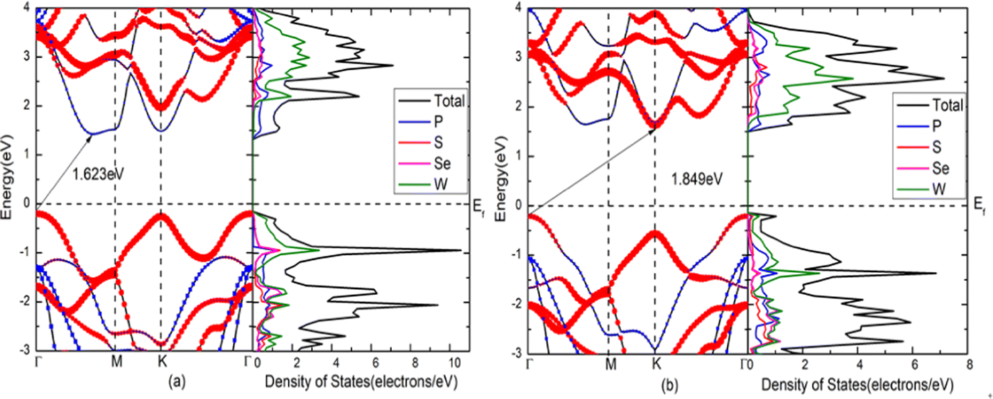 | ||
| Fig. 3 Band structures and the projected density of states for heterostructures. (a) blue-P/WSeS; (b) blue-P/WSSe heterostructures. | ||
To further study the optoelectronic properties of the blue-P/WSeS heterostructure, the work function Φ of sublayers is calculated to discuss the charge transfer between these two layers. According to the definition of Φ, it can be calculated by the formula Φ = EVAC − EVBM; where EVAC and EVBM are the energies corresponding to the vacuum potential and VBM, respectively. Our calculated Φ for the blue-P and Janus-WSeS monolayer are 6.112 and 5.692 eV, respectively. The corresponding work function differences ΔΦ across the interface is about 0.42 eV, which results in the electrons transfer from the Janus-WSeS layer to the blue-P layer and an intrinsic built-in electric field (Ein) established in the blue-P/WSeS interface. The built-in electric field will further facilitate the separation of photoexcited electron–hole pairs in the blue-P/WSeS heterostructure. In addition, the planar average electrostatic potential of the blue-P/WSeS along the c-axial direction was calculated and is presented in Fig. 4(a). It can be seen that there exists an electrostatic potential difference across the interface. Due to the higher electronegativity of the blue-P layer, the depth of potential for the blue-P layer is deeper than that of the Janus-WSeS by about 1.4 eV.
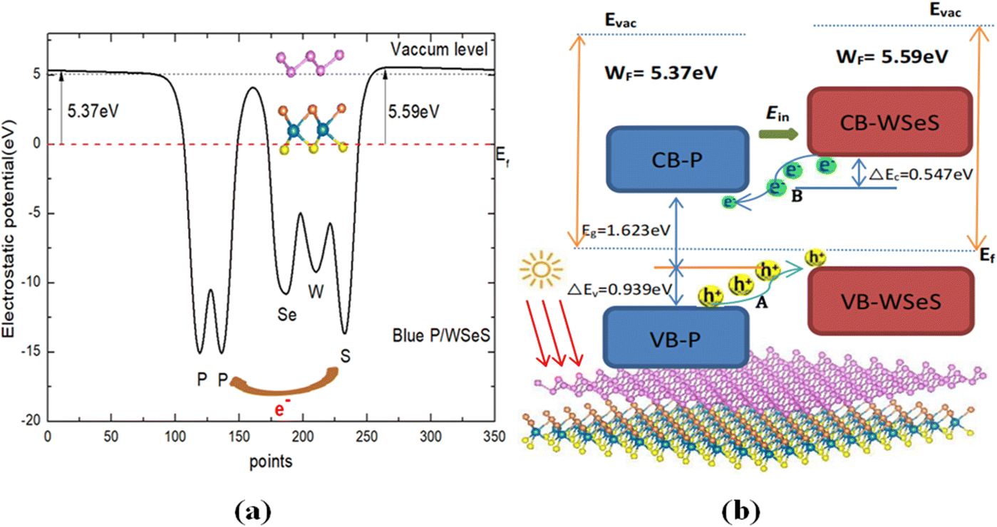 | ||
| Fig. 4 (a) Planar average electrostatic potential of the blue-P/WSeS along the c-axial direction. (b) Schematic plot of the band alignment between the two layers in blue-P/WSeS and the migration of photogenerated electrons and holes at the interface. | ||
As shown in Fig. 4(b), we also present the schematic plot of the migration of photogenerated electrons and holes at the blue-P/WSeS interface. It can be seen that, if irradiated by light, there would be three significant paths for charge carrier flow at the interface of the heterostructure:
(1) the photoexcited holes transit from the blue-P to WSeS layer between their VBMs (process A in Fig. 4(b)); (2) the photoexcited electrons transit from the Janus-WSeS to blue-P layer between their CBMs (process B in Fig. 4(b)). These two paths result in charge separation, and the last path leads to carrier recombination. The built-in electric field formed at the blue-P/WSeS interface will further promote these two processes. These two paths for charge carriers and the existence of the built-in electric field make the blue-P/WSeS heterostructure a potential photocatalyst. Then, we studied whether it could be used as a catalyst for water splitting. For this reason, we calculated its band edges.
Calculated results show that the band edges of the blue-P/WSeS heterostructure relative to the vacuum level are located at −4.17 eV (CBM) and −5.79 eV (VBM), respectively. Those wholly straddle the water reduction potentials (EH+/H2: −4.44 eV) and oxidation potential (EO2/H2O: −5.67 eV) at pH = 0.43 So, the redox reaction of water splitting can occur in different layers of the blue-P/WSeS heterostructure: water oxidation occurs in the Janus-WSeS layer (the photoexcited holes collected in the WSeS layer drive the generation of oxygen by the reaction: 2H2O + 4h+ → O2 + 4H+), meanwhile water reduction takes place in the blue-P layer (the photoexcited electrons collected in the blue-P layer drive the hydrogen reduction reaction generating hydrogen by 4H+ + 4e− → 2H2). Thus, the blue-P/WSeS heterostructure could be considered a potential photocatalyst for water splitting.
3.3 Tuning of optoelectronic properties via biaxial strain
To understand the effect of strain on the blue-P/WSeS heterostructure, a biaxial strain parallel to the stacking layers is applied on the heterostructure from −6% to 6% to investigate the evolution of structure and optoelectronic properties. In Fig. 5, the energy bands under different strains have been presented. Compared to the case without strain (as shown in Fig. 3(a)), it can be seen that not only can strain affect the size of the band gap, but also the positions of VBM and CBM, i.e., the band alignment. A small negative strain leads to a decreased direct band gap, but a small positive strain only reduces the indirect band gap while the corresponding high symmetry points of VBM and CBM remain unchanged. The strain with a larger absolute value will result in the band alignment of the blue-P/WSeS heterostructure change from type-II to type-I. According to the requirements, we can choose a suitable strain to adjust the band of the heterostructure. In Fig. 6, we present the band edges of the blue-P/WSeS heterostructure relative to the vacuum level at different strains. It can be seen that its band gap spans the potential of oxidation (O2/H2O) and reduction (H+/H2) reactions under a stress from −2% to 2%. In this strain range, the energetically favorable band edge positions for the blue-P/WSeS heterostructure make them a potential catalyst for water splitting at pH = 0.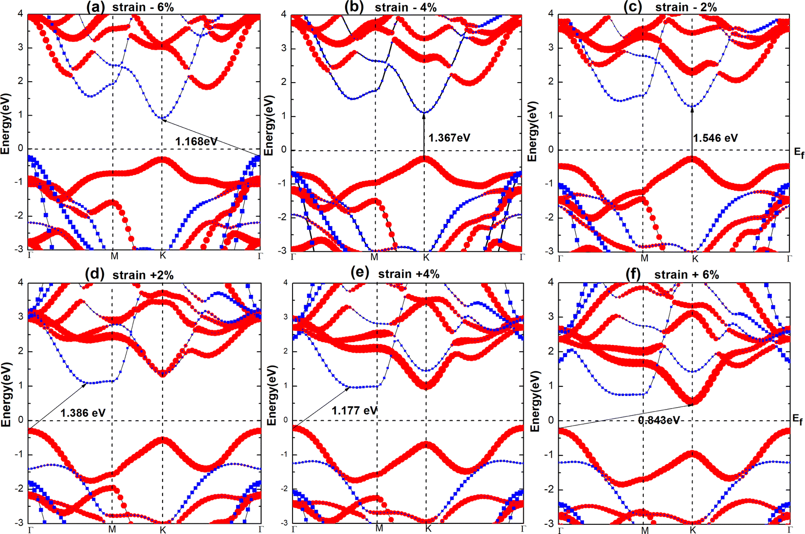 | ||
| Fig. 5 Band structures of blue-P/WSeS heterostructure under different strains. | ||
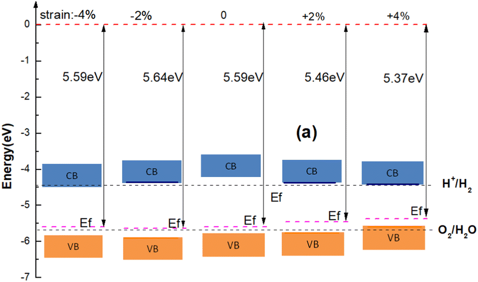 | ||
| Fig. 6 The band edges of the blue-P/WSeS heterostructure relative to the vacuum level at different strains. | ||
In Fig. 7(a), we present the total energy and band gap of the blue-P/WSeS heterostructure as a variation of strain. The total energy reaches the global minimum when no strain is applied to the heterostructure, which is consistent with previous studies.6,41 The band gap decreases with the increase in the absolute value of the applied strain. In addition, we explore the optical absorption coefficient and band edges of the blue-P/WSeS heterostructure under different strains. In Fig. 7(b), it can be seen that it has a considerable light absorption coefficient in the visible and ultraviolet regions. The absorption coefficient reaches its maximum at the ultraviolet (UV) region under different strains. Investigations of optical properties under strain show that negative strain will enhance the absorption of UV light and weaken the absorption of visible light; with positive strain, it is the opposite case. Combined with Fig. 6 and 7(b), the energetically favorable band edge positions and strong absorption in UV light for the blue-P/WSeS heterostructure make the blue-P/WSeS heterostructure a potential UV irradiation catalyst for water splitting at pH = 0.
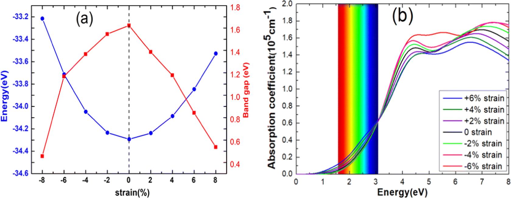 | ||
| Fig. 7 (a) The total energy, band gap, and (b) the optical absorption coefficient of blue-P/WSeS heterostructure changed as strain. | ||
4. Conclusion
To sum up, we designed several blue-P/Janus-WSeS and blue-P/Janus-WSSe vdW heterostructures and selected the one with the more stable structure and better performance—the AB stacking blue-P/Janus-WSeS heterostructure. Then, first principle calculations were carried out to investigate the electronic and optical properties of this heterostructure. Results show that this heterostructure presents an intrinsic type-II band alignment. The analysis of the band alignment shows this heterostructure is a potential photocatalyst material for water splitting. Irradiated by light, the photoexcited holes collect and water oxidation occurs in the Janus-WSeS layer; meanwhile, the photoexcited electrons collect and water reduction takes place in the blue-P layer. Then, we further explored the effect of biaxial strain on optoelectronic properties. Results show it is an effective method to regulate the energy band of the heterostructure. A small negative strain will lead to a decreased direct band gap, but a small positive strain only reduces the indirect band gap while the corresponding high symmetry points of VBM and CBM remain unchanged. The strain with a larger absolute value will result in the band alignment of this blue-P/WSeS heterostructure change from type-II to type-I. At the end of this work, we investigated the absorption coefficient of the heterostructure at different strains. Results show that the AB stacking blue-P/Janus-WSeS heterostructure has a considerable light absorption coefficient in the visible and ultraviolet regions, and the maximum absorption coefficient occurs in the UV region. Negative strain could enhance the absorption of UV light, while positive strain would weaken the absorption of UV light. Favorable band edge positions and strong absorption in UV light make this blue-P/WSeS vdW heterostructure a potential visible and UV light irradiation catalyst for water splitting.Conflicts of interest
There are no conflicts to declare.Acknowledgements
Project supported by the Foundation of LCP (Laboratory of Computational Physics) (Grant No. 6142A05210101), the Key Research & Development and promotion projects in Henan Province (Grant No. 222102230081, 202102210205), and the Key Research Project of Higher Education of Henan Province (Grant No. 21B140011).References
- K. S. Novoselov, A. K. Geim, S. V. Morozov, D. Jiang, Y. Zhang, S. V. Dubonos, I. V. Grigorieva and A. A. Firsov, Electric Field Effect in Atomically Thin Carbon Films, Science, 2004, 306, 666 CrossRef CAS PubMed.
- J. Li, Z. Li, X. Liu, C. Li, Y. Zheng, K. W. K. Yeung, Z. Cui, Y. Liang, S. Zhu, W. Hu, Y. Qi, T. Zhang, X. Wang and S. Wu, Interfacial engineering of Bi2S3/Ti3C2Tx MXene based on work function for rapid photo-excited bacteria-killing, Nat. Commun., 2021, 12, 1224 CrossRef CAS PubMed.
- J. Son, A. Hashmi and J. Hong, Optical properties of g-C4N3/BN bilayer film: A first-principles study, J. Korean Phys. Soc., 2015, 67, 1624 CrossRef CAS.
- J. Cui, S. Liang and J. Zhang, A multifunctional material of two-dimensional g-C4N3/graphene bilayer, Phys. Chem. Chem. Phys., 2016, 18, 25388 RSC.
- B. You, X. Wang and W. Mi, Prediction of spin-orbital coupling effects on the electronic structure of two dimensional van der Waals heterostructures, Phys. Chem. Chem. Phys., 2015, 17, 31253 RSC.
- L. Lin, M. Lou, S. Li, X. Cai, Z. Zhang and H. Tao, Tuning electronic and optical properties of two–dimensional vertical van der Waals arsenene/SnS2 heterostructure by strain and electric field, Appl. Surf. Sci., 2022, 572, 151209 CrossRef CAS.
- X. Zhang, Z. Zhang, D. Wu, X. Zhang, X. Zhao and Z. Zhou, Computational Screening of 2D Materials and Rational Design of Heterojunctions for Water Splitting Photocatalysts, Small Methods, 2018, 2, 1700359 CrossRef.
- J. Guan, Z. Zhu and D. Tomanek, Phase coexistence and metal-insulator transition in few-layer phosphorene: a computational study, Phys. Rev. Lett., 2014, 113, 046804 CrossRef CAS PubMed.
- B. Peng, H. Zhang, H. Shao, K. Xu, G. Ni, J. Li, H. Zhu and C. M. Soukoulis, Chemical intuition for high thermoelectric performance in monolayer black phosphorus, α-arsenene and aW-antimonene, J. Mater. Chem. A, 2018, 6, 2018 RSC.
- M. Z. Rahman, C. W. Kwong, K. Davey and S. Z. Qiao, Correction: 2D phosphorene as a water splitting photocatalyst: fundamentals to applications, Energy Environ. Sci., 2016, 9, 1513 RSC.
- K. F. Mak and J. Shan, Photonics and optoelectronics of 2D semiconductor transition metal dichalcogenides, Nat. Photonics, 2016, 10, 216 CrossRef CAS.
- W. Zheng, B. Zheng, C. Yan, Y. Liu, X. Sun, Z. Qi, T. Yang, Y. Jiang, W. Huang, P. Fan, F. Jiang, W. Ji, X. Wang and A. Pan, Direct Vapor Growth of 2D Vertical Heterostructures with Tunable Band Alignments and Interfacial Charge Transfer Behaviors, Adv. Sci., 2019, 6, 1802204 CrossRef PubMed.
- J. Wong, D. Jariwala, G. Tagliabue, K. Tat, A. R. Davoyan, M. C. Sherrott and H. A. Atwater, High Photovoltaic Quantum Efficiency in Ultrathin van der Waals Heterostructures, ACS Nano, 2017, 11, 7230 CrossRef CAS PubMed.
- M. Z. Rahman, C. W. Kwong, K. Davey and S. Z. Qiao, 2D phosphorene as a water splitting photocatalyst: fundamentals to applications, Energy Environ. Sci., 2016, 9, 709 RSC.
- A. Gupta, T. Sakthivel and S. Seal, Recent development in 2D materials beyond graphene, Prog. Mater. Sci., 2015, 73, 44 CrossRef CAS.
- Y. Xu, W. Zhao, R. Xu, Y. Shi and B. Zhang, Synthesis of ultrathin CdS nanosheets as efficient visible-light-driven water splitting photocatalysts for hydrogen evolution, Chem. Commun., 2013, 49, 9803 RSC.
- W. Ma, S. Hao, L. Zhang, B. Lv, G. Zhao, J. Huang and X. Xu, 2D WS2 co-catalysts induce the growth of CdS and enhance the photocatalytic performance, CrystEngComm, 2021, 23, 4451 RSC.
- H. Qiao, Y. Zhang, Z.-H. Yan, L. Duan, L. Ni, J.-B. Fan and A. type-II, GaN/InS van der Waals heterostructure with high solar-to-hydrogen efficiency of photocatalyst for water splitting, Appl. Surf. Sci., 2022, 604, 154602 CrossRef CAS.
- D. Ren, K. Qian, Q. Li, Y. Zhang and T. Zhang, The Electronic and Optical Properties of Vertically Stacked GaN-WS2 Heterostructure, J. Wuhan Univ. Technol., Mater. Sci. Ed., 2022, 37, 28 CrossRef CAS.
- G. Wang, W. Tang, W. Xie, Q. Tang, Y. Wang, H. Guo, P. Gao, S. Dang and J. Chang, Type-II CdS/PtSSe heterostructures used as highly efficient water-splitting photocatalysts, Appl. Surf. Sci., 2022, 589, 152931 CrossRef CAS.
- Z. Zhao, C. Yang, Z. Cao, Y. Bian, B. Li and Y. Wei, Two-dimensional ZnO/BlueP van der Waals heterostructure used for visible-light driven water splitting: A first-principles study, Spectrochim. Acta, Part A, 2022, 278, 121359 CrossRef CAS PubMed.
- I. Shahid, S. Ahmad, N. Shehzad, S. Yao, C. V. Nguyen, L. Zhang and Z. Zhou, Electronic and photocatalytic performance of boron phosphide-blue phosphorene vdW heterostructures, Appl. Surf. Sci., 2020, 523, 146483 CrossRef CAS.
- N. Shehzad, I. Shahid, S. Yao, S. Ahmad, A. Ali, L. Zhang and Z. Zhou, A first-principles study of electronic structure and photocatalytic performance of two-dimensional van der Waals MTe2–As (M = Mo, W) heterostructures, Int. J. Hydrogen Energy, 2020, 45, 27089 CrossRef CAS.
- A. K. Sharma and A. K. Pandey, Blue Phosphorene/MoS2 Heterostructure Based SPR Sensor With Enhanced Sensitivity, IEEE Photonics Technol. Lett., 2018, 30, 595 CAS.
- H. Bian, H. Duan, J. Li, F. Chen, B. Cao and M. Long, Electronic and magnetic properties of the transition-metal absorbed blue-phosphorus/MoS2 heterostructure: A first-principles investigation, AIP Adv., 2019, 9, 065207 CrossRef.
- J. Huang, Y. Peng and X. Han, Tuning the electronic and optical properties of Blue P/MoSeS and Blue P/MoSSe van der Waals heterostructure via biaxial strain, Chem. Phys. Lett., 2021, 773, 138622 CrossRef CAS.
- J. Wang, Y. Huang, F. Ma, J. Zhang, X. Wei and J. Liu, Strain engineering the electronic and photocatalytic properties of WS2/blue phosphene van der Waals heterostructures, Catal. Sci. Technol., 2021, 11, 179 RSC.
- L. Zhang, L. Huang, T. Yin and Y. Yang, Strain-Induced Tunable Band Offsets in Blue Phosphorus and WSe2 van der Waals Heterostructure, Crystals, 2021, 11, 470 CrossRef CAS.
- A. Y. Lu, H. Zhu, J. Xiao, C. P. Chuu, Y. Han, M. H. Chiu, C. C. Cheng, C. W. Yang, K. H. Wei, Y. Yang, Y. Wang, D. Sokaras, D. Nordlund, P. Yang, D. A. Muller, M. Y. Chou, X. Zhang and L. J. Li, Janus monolayers of transition metal dichalcogenides, Nat. Nanotechnol., 2017, 12, 744 CrossRef CAS PubMed.
- Y. Qin, M. Sayyad, A. R. Montblanch, M. S. G. Feuer, D. Dey, M. Blei, R. Sailus, D. M. Kara, Y. Shen, S. Yang, A. S. Botana, M. Atature and S. Tongay, Reaching the Excitonic Limit in 2D Janus Monolayers by In Situ Deterministic Growth, Adv. Mater., 2022, 34, 2106222 CrossRef CAS PubMed.
- Y. Luo, S. Wang, H. Shu, J.-P. Chou, K. Ren, J. Yu, M. Sun and A. MoSSe/blue, phosphorene vdw heterostructure with energy conversion efficiency of 19.9% for photocatalytic water splitting, Semicond. Sci. Technol., 2020, 35, 125008 CrossRef CAS.
- K. Ren, S. Wang, Y. Luo, J.-P. Chou, J. Yu, W. Tang and M. Sun, High-efficiency photocatalyst for water splitting: a Janus MoSSe/XN (X
![[thin space (1/6-em)]](https://www.rsc.org/images/entities/char_2009.gif) = Ga, Al) van der Waals heterostructure, J. Phys. D: Appl. Phys., 2020, 53, 185504 CrossRef CAS.
= Ga, Al) van der Waals heterostructure, J. Phys. D: Appl. Phys., 2020, 53, 185504 CrossRef CAS. - G. Kresse and J. Hafner, Ab initio molecular dynamics for open-shell transition metals, Phys. Rev. B: Condens. Matter Mater. Phys., 1993, 48, 13115 CrossRef CAS PubMed.
- G. Kresse and J. Furthmüller, Efficient iterative schemes for ab initio total-energy calculations using a plane-wave basis set, Phys. Rev. B: Condens. Matter Mater. Phys., 1996, 54, 11169 CrossRef CAS PubMed.
- S. Grimme, J. Antony, S. Ehrlich and H. Krieg, A consistent and accurate ab initio parametrization of density functional dispersion correction (DFT-D) for the 94 elements H-Pu, J. Chem. Phys., 2010, 132, 154104 CrossRef PubMed.
- S. Grimme, S. Ehrlich and L. Goerigk, Effect of the damping function in dispersion corrected density functional theory, J. Comput. Chem., 2011, 32, 1456 CrossRef CAS PubMed.
- A. V. Krukau, O. A. Vydrov, A. F. Izmaylov and G. E. Scuseria, Influence of the exchange screening parameter on the performance of screened hybrid functionals, J. Chem. Phys., 2006, 125, 224106 CrossRef PubMed.
- H. J. Monkhorst and J. D. Pack, Special points for Brillouin-zone integrations, Phys. Rev. B: Solid State, 1976, 13, 5188 CrossRef.
- J. Sun, H.-T. Wang, J. He and Y. Tian, Ab initioinvestigations of optical properties of the high-pressure phases of ZnO, Phys. Rev. B: Condens. Matter Mater. Phys., 2005, 71, 125132 CrossRef.
- Q.-J. Liu, N.-C. Zhang, F.-S. Liu and Z.-T. Liu, Structural, electronic, optical, elastic properties and Born effective charges of monoclinic HfO2 from first-principles calculations, Chin. Phys. B, 2014, 23, 047101 CrossRef.
- B. Amin, T. P. Kaloni and U. Schwingenschlögl, Strain engineering of WS2, WSe2, and WTe2, RSC Adv., 2014, 4, 34561 RSC.
- H. Shu, A type-II blue phosphorus/MoSe2 van der Waals heterostructure: improved electronic and optical properties via vertical electric field, Mater. Adv., 2020, 1, 1849 RSC.
- A. K. Singh, K. Mathew, H. L. Zhuang and R. G. Hennig, Computational Screening of 2D Materials for Photocatalysis, J. Phys. Chem. Lett., 2015, 6, 1087 CrossRef CAS PubMed.
| This journal is © The Royal Society of Chemistry 2022 |