
 Open Access Article
 This Open Access Article is licensed under a Creative Commons Attribution-Non Commercial 3.0 Unported Licence
An overview on the role of ZnTe as an efficient interface in CdTe thin film solar cells: a review
Deepak
Suthar
,
Sakshi
Chuhadiya
,
Ritika
Sharma
,
Himanshu
and
M. S.
Dhaka
 *
*
Department of Physics, Mohanlal Sukhadia University, Udaipur-313001, India. E-mail: msdhaka75@yahoo.co.in; msdhaka@mlsu.ac.in
First published on 31st October 2022
Abstract
The present era of cutting edge technology requires environmentally friendly alternative energy resources due to the limited fuel reserves and the emission of pollutants associated with the use of conventional resources such as fossil fuels. Since the invention of CdTe-based solar cells, they have become potential suitable alternatives and competitors to silicon solar cells owing to their cost effectiveness and stability. Thus, the development of CdTe thin film solar cells has gained significant attention due to their potential roles as sustainable energy sources. To develop higher efficiency CdTe-based thin film solar cell devices, typically, a zinc telluride (ZnTe) layer is employed as an essential interface between the CdTe absorber and metal contact. The superiority of the ZnTe back contact improves the shunting pathway to the motion of charge carriers, which eventually enhances the device performance. With the use of a supporting CdSeTe absorber and magnesium-doped zinc oxide (MZO) optical window together with a ZnTe back contact, these devices are commonly utilized not only in single junction devices but also tandem devices. This review presents major improvements in the power conversion efficiency of CdTe thin film solar cells in detail with special reference to the ZnTe back contact layer. It also highlights various thin film deposition techniques together with the impact of doping and post-deposition treatment on ZnTe thin films to enhance the related properties, followed by the importance of the present study.
 Deepak Suthar | Deepak Suthar, a PhD scholar at the Department of Physics, Mohanlal Sukhadia University, Udaipur, India, has been a Junior Research Fellow in the Research and Development Project funded by the Department of Science and Technology, Rajasthan, India. He has authored 15 research papers in reputed international journals of high visibility. His research is mainly focused on the growth and characterization of semiconducting materials and ZnTe back contact-comprised CdTe solar cell devices. |
 Sakshi Chuhadiya | Sakshi Chuhadiya, a PhD scholar at the Department of Physics, Mohanlal Sukhadia University Udaipur, India, is currently Senior Research Fellow awarded by the Council of Scientific and Industrial Research, India. She has authored several papers in reputed international journals of high impact including Coordination Chemistry Reviews. Her current research is mainly focused on the design, synthesis, and applications of metal organic frameworks in solar cell devices. |
 Ritika Sharma | Ritika Sharma, a PhD scholar at the Department of Physics, Mohanlal Sukhadia University Udaipur, India, is currently a Junior Research Fellow in the Research and Innovation Project funded under RUSA 2.0 Scheme by the Govt. of India and Govt. of Rajasthan. She has authored several research papers in reputed international journals of high visibility such as Solar Energy. Her current research interest includes thin films, CdZnTe and perovskite solar cell devices. |
 Himanshu | Dr Himanshu, a recipient of the INSPIRE Fellowship awarded by the Department of Science and Technology, India, received his PhD from the Mohanlal Sukhadia University Udaipur, India. He has authored more than 40 research papers in reputed international journals of high impact and visibility including AIP conference proceedings and has visited the UAE and UK. His research domain mainly covers thin films and solar cell materials. |
 M. S. Dhaka | Dr M. S. Dhaka, a recipient of the Raman Postdoctoral Fellowship at Iowa State University, USA, is currently a Professor of Physics at Mohanlal Sukhadia University, Udaipur, India. He supervised four PhDs and has been principal investigator of three research projects funded by UGC, India, DST, Rajasthan and SERB, India. Dr Dhaka has authored more than 100 research papers in reputed international journals of high visibility including AIP and IEEE conference proceedings. His current research mainly focuses on thin films, solar cells, metal organic frameworks and thin film solid oxide fuel cells. He has visited the UK, Norway and USA. |
1. Introduction and solar cell generations
In the present era, the major challenges include the fulfillment of the increasing energy demand in every sector across the globe including power. Although conventional energy sources such as coal, oil, and natural gases fulfill the maximum requirement of total energy globally, these resources affect the environment and lifestyle of human beings by emitting pollutants, e.g., the burning of fossil fuels produces greenhouse gases and many hazardous gases, which contribute to global warming. The conventional and non-renewable energy resources have been depleted with time due to their limited availability, and therefore, the search for environmentally clean and safe renewable energy resources should be the focus. Over the past few decades, several renewable routes have been considered as cleaner energy sources, which can play a significant role to meet the future energy needs of the society. The excellent use of these resources not only reduces the environmental impact and creates minimum secondary waste but also sustainability, considering the current and future social and economic necessities. The global energy requirement is rising rapidly due to technological advancements together with population explosion, and hence, it is essential to develop reliable, cost-effective, and never-ending renewable energy sources to fulfill the required energy demands arising in the future.1–8 An overview of the different types of renewable and non-renewable energy resources is pictorially presented in Fig. 1.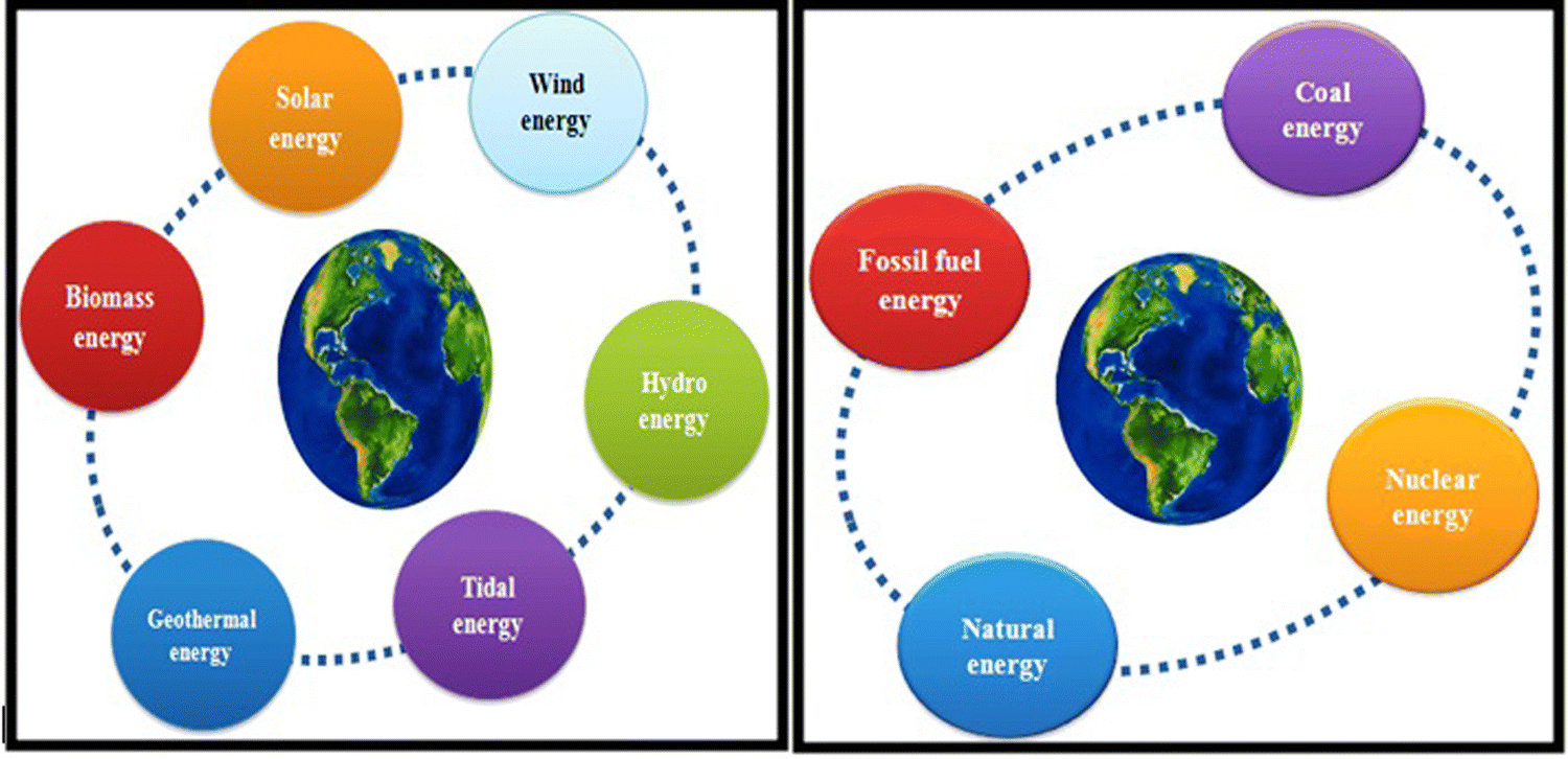 | ||
| Fig. 1 Pictorial view of renewable and non-renewable energy sources. | ||
Solar energy, among the different types of renewable energy sources such as wind, hydro, tidal, geothermal, and biomass, is a promising and free energy source, with significant potential to address the long-term issues associated with the energy crisis. The sun is a powerful source of solar energy, and the primary forms of solar energy are heat and light. Sunlight is absorbed and transformed by the environment in various ways. Solar energy has several outstanding features, e.g., it does not have any destructive impact on the ecosystem, is effectively employed for industrial operations, and it is easily affordable, not exhaustible, and provides increasing output in terms of power conversion efficiencies compared to other energy sources.9–16 The significant features associated with solar energy technology are depicted in Table 1.
| Significant feature(s) | Comment(s) |
|---|---|
| Eco-friendly nature | Unlike conventional power sources, solar system produces no harmful emissions to the environment. |
| Silent | Solar panels do not make any noise during the process of converting sunlight into electricity. |
| Durability | Solar panels do not contain any movable parts, and therefore, the probability of them being damaged is very low. |
| Cost effectiveness | Solar energy is more cost effective compared to other energy sources based on several aspects. |
| Solid home investment | Solar energy saves money and the investment made on solar panels add value to the home. |
| Ahead of the curve | The future of the world would be renewable and clean energy driven. The conversion of solar energy into electricity would be a step ahead to meet the energy need of society. |
| Low-maintenance | Once solar panels have been installed and their efficiency is maximized, and subsequently they require very little maintenance, although each technology has a certain lifetime. |
Considering the sustainable and abundant availability of solar irradiance on the Earth's surface throughout the year, persistent efforts have been devoted thus far to solar photovoltaic research to develop high-performance and efficient solar cell devices.17 Solar cell device is a p–n junction diode and works on the principle of the photovoltaic effect, which explains the direct conversion of light into electrical energy.18 In 1954, the first silicon solar cell was demonstrated at Bell Laboratories, which showed ∼6% power conversion efficiency (PCE). Thereafter, continuous research efforts have been made to overcome the complexity in power conversion efficiency and cost effectiveness by demonstrating high-performance devices to meet the energy demands. Solar cell devices are typically categorized into first-, second-, and third-generations based on their development history and absorbers, which are pictorially shown in Fig. 2 and described briefly herein.19–23 The single/monocrystalline silicon, multi/polycrystalline silicon and GaAs solar cells are considered first-generation solar cells. The second generation comprises thin film-based solar cells, which emerged with low production cost and minimal material consumption. It is noteworthy that the semiconductor materials (especially absorbers) used in the second-generation solar cells have a direct band gap, whereas the first-generation solar cells using silicon material have an indirect band gap. The second generation includes amorphous silicon (a-Si) solar cells, cadmium telluride (CdTe) solar cells, and copper indium gallium diselenide (CIGS) solar cells. The third generation comprises dye-sensitized solar cells (DSSCs), organic solar cells (OSCs), quantum dot solar cells (QDSCs), and perovskite solar cells (PSCs).19–28
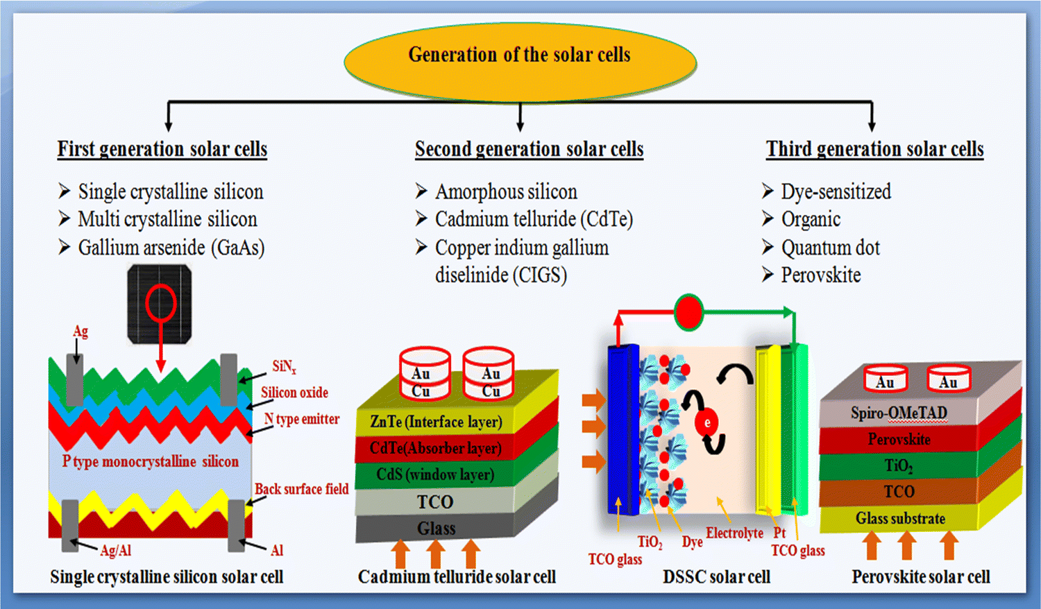 | ||
| Fig. 2 Classification of solar cells based on their generation. | ||
A concise explanation of the different solar photovoltaic technologies is presented herein, where the devices are recognized and named according to their absorber layers.
1.1 First-generation solar cells
This generation includes silicon wafer-based solar cells, which are also known as conventional or traditional solar cells. As stated, the first silicon-based solar cell was developed in 1954 at Bell Laboratories with a PCE of 6%, and thereafter, substantial research on enhancing the PCE was carried out. First-generation solar cells are of two types: (a) single crystalline silicon solar cells and (b) polycrystalline silicon solar cells.1.2 Second-generation solar cells
These are thin film-based devices having a low production cost and minimal material consumption. As stated, there are three types of solar cells in this generation, as follows: (a) amorphous silicon (a-Si) solar cells, (b) cadmium telluride (CdTe) solar cells, and (c) copper indium gallium diselenide (CuInxGa1−xSe2, i.e., CIGS) solar cells.1.3 Third-generation solar cells
The high production cost of first-generation solar cells and the limited availability of materials for second-generation solar cells have invited a new generation, which emerged and recognized as the third generation of solar cells. Third-generation solar cells are naturally different from the earlier explained first and second generations including device design evolution and interface engineering. The third generation comprises several solar cell classes, which are also explained herein.Each generation of solar cells has certain merits and drawbacks and the performance of the device is affected by the properties of their constituents and growth conditions.
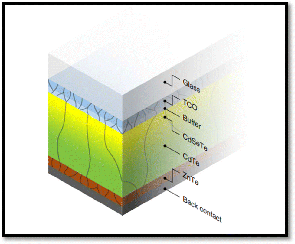
Among the different types of solar cells, thin film solar cell technology has gained huge attention due to its incredibly controlled production costs through the reduced consumption of constituent layer materials by optimizing the thickness and other conditions. Thin film solar cells are promising devices for global photovoltaics due to their wide diversity of choices in terms of device fabrication and design. In the fabrication of thin film solar cells, various types of substrates can be applied in accordance with the device architecture. To develop constituent layers, i.e., absorber, window/buffer and interface layers, a variety of strategies has been developed, which can be categorized as physical and chemical routes, which have their own merits and disadvantages. The deposition techniques and conditions allow tailoring and engineering the properties of the different constituent layers of solar cells to improve the device performance. A true understanding and knowledge of the thin film deposition processes can assist in achieving high performances. The growth and characterization to fabricate the constituent layers with simple manufacturing processes need to be studied.41–46 Among the second-generation solar cells, for the development of CdTe thin film solar cell devices, the typical architecture used thus far is glass/TCO/CdS/CdTe/ZnTe/metal contact, while in recent years, due to the evolution of materials, modified architecture as Glass/MZO/CdSeTe/CdTe/ZnTe/metal contact has also been applied to achieve an elevated performance, where MZO (magnesium-doped zinc oxide) is used as a window layer instead of the conventional CdS together with CdSeTe (CdSexTe1−x)/CdTe as a graded absorber. An illustration of the typical CdSeTe/CdTe architecture device is provided in Fig. 3 together with its energy band diagram and the features of thin film solar cells.
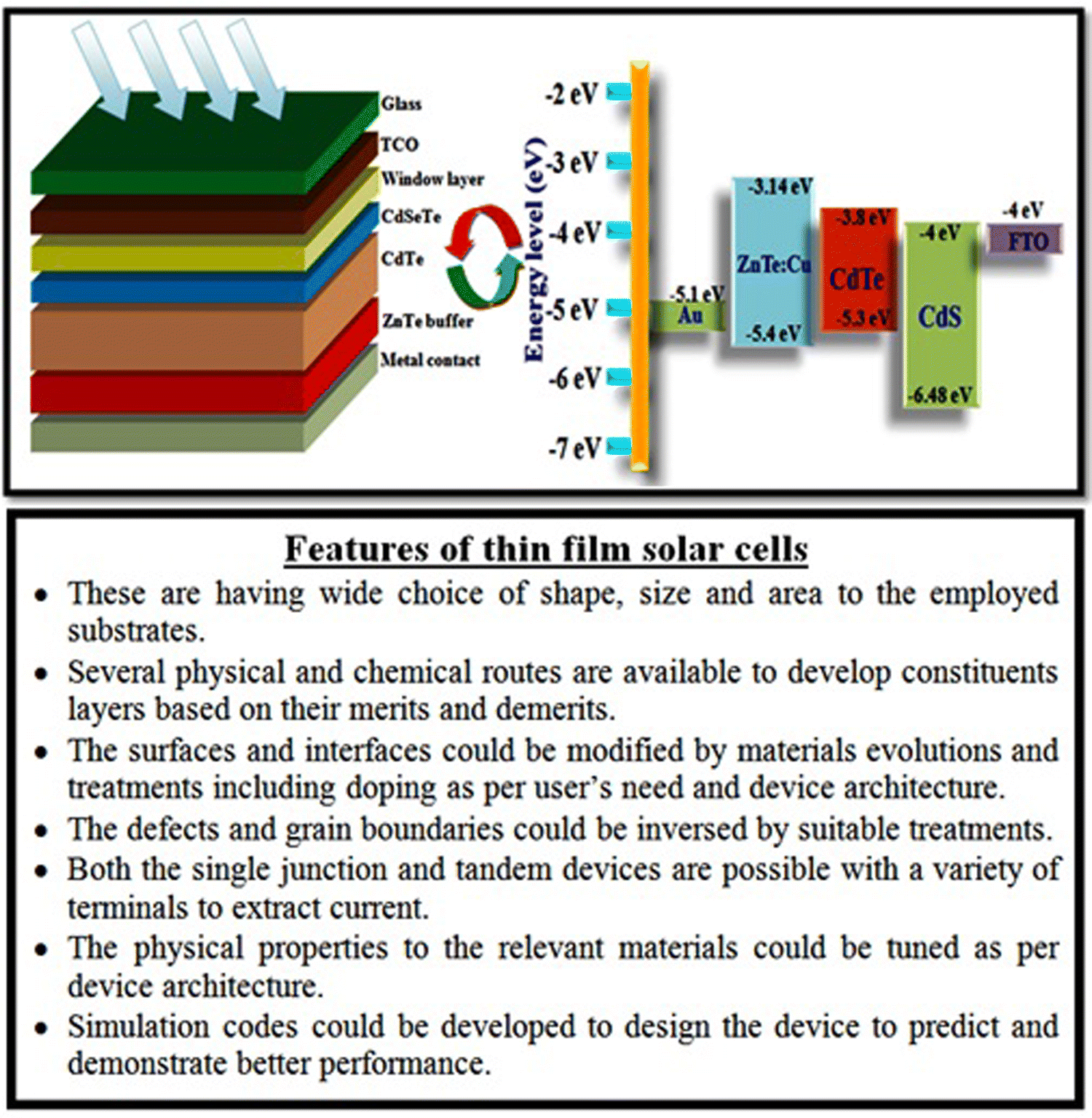 | ||
| Fig. 3 Pictorial view of the CdSeTe/CdTe solar cell device architecture, typical energy band diagram and features of thin film solar cells. | ||
CdTe solar cells are widely used because CdTe is an emerging material with unique properties such as direct optical energy band gap (1.45 eV), high chemical stability, and large absorption coefficient.47–54 In CdTe-based thin film solar cells, mismatching of the CdTe valence band level and electrode metal work function results in open circuit voltage loss, and thus the desired efficiency cannot be achieved. To enable facile hole transportation, ZnTe is employed as a back contact interface, which also resolves issue of the presence of a Schottky barrier due to the high electron affinity and lower charge carrier concentration of the CdTe material.
Traditionally, a CdS window layer is employed to develop CdTe solar cells, where during the CdTe deposition and CdCl2 treatment, interdiffusion happens at the CdS/CdTe interface, and consequently CdS1−yTey is alloyed in the window layers and CdTe1−xSx in the CdTe absorber, where CdS1−yTey is not only highly defective but photo-inactive55 too and the CdTe1−xSx alloy reduces band gap. The diffusion of S into CdTe enhances the photocurrent collection in longer wavelength regions (825–865 nm). Although to obtain a suitable band gap, a significant amount of S should be incorporated in CdTe but the solubility of CdS in CdTe is established to be very low due to the large size mismatch between S and Te.56,57 Se has lower size mismatch with Te than S, and consequently CdSe has greater solubility in CdTe compared to CdS.55 The band gap in the CdTe1−xSex alloy is reduced from 1.4 eV to 1.32 eV and the photocurrent is improved, which eventually leads to an increment in power conversion efficiency.58 The recombination loss associated with the back surface of CdTe devices can also be reduced by inserting the wider band gap ZnTe as the back contact layer between the absorber and metal contact, and compliance work demonstrated a power conversion efficiency of ∼20%.59
To improve the performance to CdTe-based solar cells, in recent years, researchers have mainly focused on two features including replacement of the traditional CdS window layer by a wide band gap and fully transparent material such as Zn1−xMgxO (ZMO)60–63 for advancement in photocurrent and the introduction of Se in CdTe to form a graded band gap CdSeTe/CdTe absorber, which can passivate the front surface to increase the carrier lifetime and absorption in the longer wavelength region simultaneously.64 An efficiency of ∼16% was reported by Samoilenko et al.65,66 by using a magnesium-doped zinc oxide (MZO) window layer in CdTe solar cells. The introduction of Se in the form of a CdSeTe layer at the interface with magnesium-doped zinc oxide (MZO) resulted in a PCE of 18.6%61 and ∼19%67 under similar conditions. Metzger et al.68 predicted a PCE of ∼20.8% by employing simulation modeling for a graded CdSeTe/CdTe absorber layer doped with arsenic (As). The recorded efficiency of 22.1% was attained by applying the architecture of glass/FTO/MZO/CdSeTe/CdTe/ZnTe/metal contact.69,70 However, further work is required to get improved the PCE of CdTe-based solar cells.
Considering the above, ZnTe is an important and environmentally friendly material, belonging to II–VI group compound semiconductors and having a wide direct band gap (2.26 eV) and low electron affinity (3.53 eV),71–81 which is suitable to increase the PCE of CdTe solar cell devices. An overview of the properties together with deposition and characterization techniques for the ZnTe thin film layers is shown in Fig. 4, which can be considered for the development of the layers and devices.
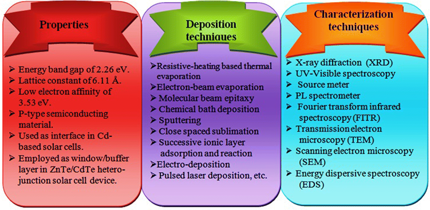 | ||
| Fig. 4 Overview of the properties, deposition and characterization techniques for ZnTe thin layers, which can be considered during material evolution and device development. | ||
A pictorial view of the unit cell of ZnTe is depicted in Fig. 5 together with the architecture of the recently developed high-performance device, where the traditional CdS layer is replaced by an eco-friendly and better optical window, i.e., magnesium-doped zinc oxide (MZO).
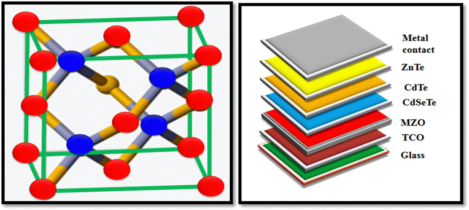 | ||
| Fig. 5 Pictorial view of the unit cell of the ZnTe and device architecture comprised of ZnTe as the back contact, where the CdS optical window is replaced by an MZO layer.65,66 | ||
Considering the current societal energy needs and device development challenges, in the present review, we explore the potential role of the ZnTe material as an efficient interface for CdTe thin-film solar cells by means of their different properties and applications in solar cells together with the relevant deposition techniques. This review is organized into the main deposition techniques used thus far, followed by an emphasis on the properties of ZnTe single layers, their potential role in device design and development with further road map to resolve challenges.
2. Deposition techniques
Thin film solar cells are comprised of several thin film layers and a variety of strategies is available thus far to develop them, where transparent conducting oxides such as indium-doped tin oxide (ITO) and fluorine-doped tin oxide (FTO)-coated glasses are used as the substrates in the superstrate device architecture and the resistive heating-based thermal evaporation technique is typically employed for the formation of the metal contact. Thin film solar cells can be developed with better efficiency and stability by optimizing the thickness and properties of their different constituent layers, i.e., window, absorber, buffer and contact layers. As stated, a variety of deposition techniques has been employed thus far to grow the constituent layers, which are classified as follows: (a) physical and (b) chemical routes, where the resistive heating thermal evaporation, electron beam evaporation, molecular beam epitaxy, sputtering, and electro-deposition techniques have been used thus far for the fabrication of ZnTe thin films,82–97 providing diverse properties. An overview of the physical and chemical routes is presented in Fig. 6, and considering their merits and drawbacks, the major deposition techniques are discussed in following section.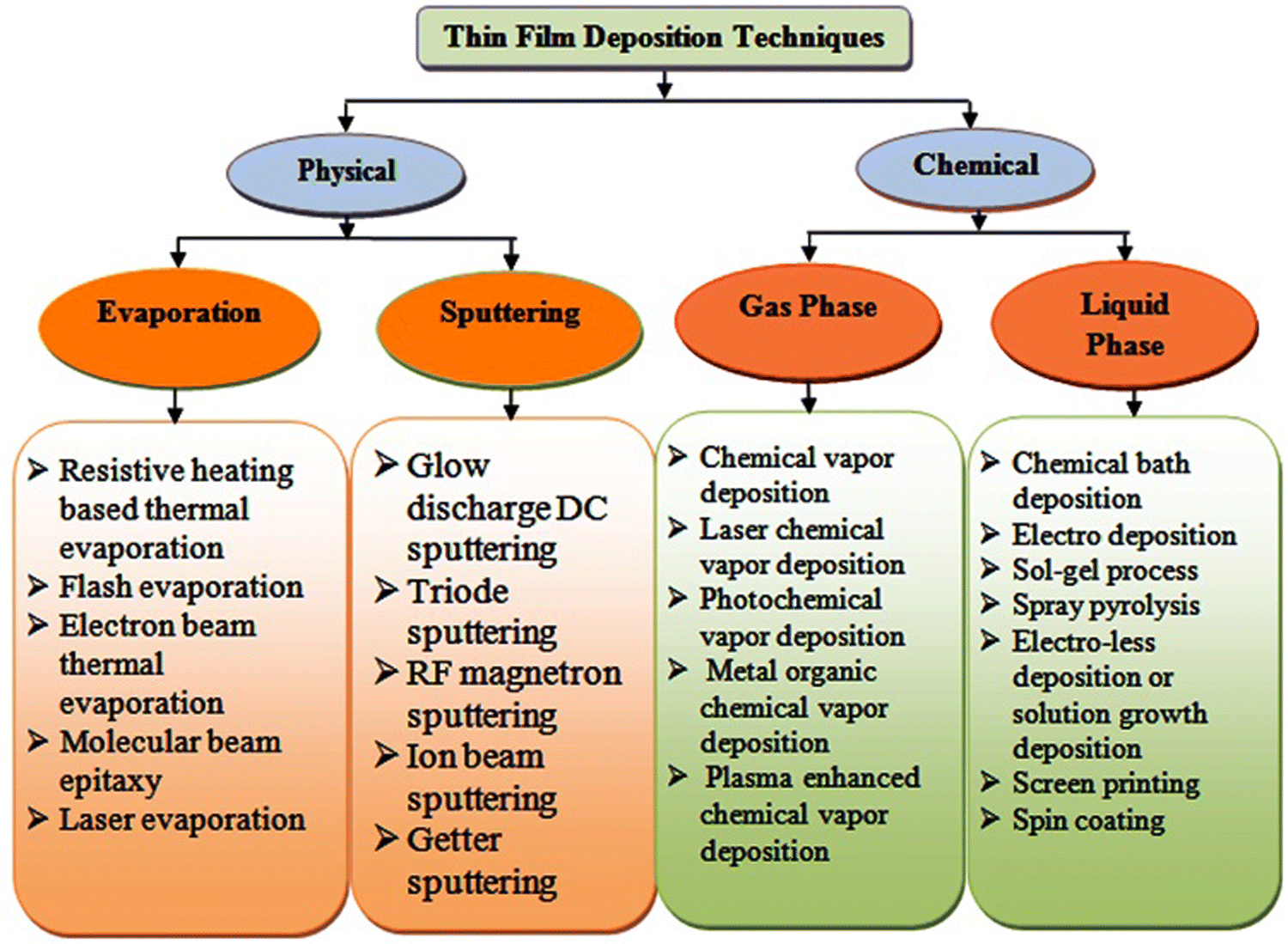 | ||
| Fig. 6 Classification of thin film deposition techniques.98 | ||
2.1 Resistive heating thermal evaporation technique
Over the years, the resistive heating thermal evaporation technique has been the most commonly used method to deposit ZnTe thin films, which is a simple, low cost, reproducible and excellent technique with optimum control over the deposition rate, substrate temperature, and film thickness.84,99–104 Numerous researchers have employed this technique to fabricate ZnTe thin films and solar cell devices.105–109 In the thermal evaporation technique, the source material is kept in a filament (boat of molybdenum, tungsten, and tantalum or tungsten basket), where the source material is heated to its melting point using electrical energy under high vacuum. A higher vacuum is required to enhance mean free path of the evaporants to minimize the contamination during the deposition due to existence of residual gases. The film growth process involves nucleation, coalescence, channels, holes, and continuous film deposition.110,111 A pictorial view of the resistive heating thermal evaporation technique together with its advantages and disadvantages is depicted in Fig. 7.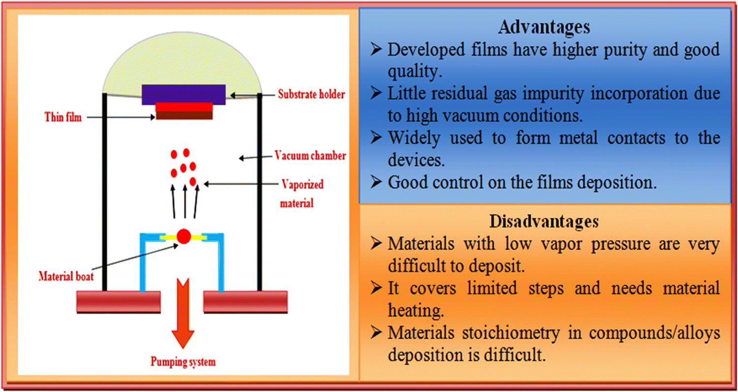 | ||
| Fig. 7 Overview of the resistive heating thermal evaporation technique together with the advantages and disadvantages of this method. | ||
Using the resistive heating thermal evaporation technique, ZnTe thin films having a thickness 300 nm were deposited on glass substrates at room temperature with vacuum of 10−6 Torr and the findings showed that it is suitable for photodetector applications.112 The impact of Cu doping on the physical properties of ZnTe thin films were investigated employing the thermal evaporation technique in the vacuum range of ∼3 × 10⁻⁴–10−7 torr, where the conductivity was varied, demonstrating DC conductive behavior and translational hopping motion at low and high frequency, respectively.99 The elemental composition also affects the properties, and accordingly stoichiometry changes were investigated for thermally evaporated 2500 nm ZnTe thin films grown at the substrate temperatures of −123 °C and 27 °C.113 The thermal evaporation technique was used to grow films with a thickness of 85 nm, 300 nm, 600 nm, and 900 nm on silicon and glass substrates114–117 and thickness of 200 nm, 400 nm, 600 nm, and 1000 nm at the growth temperature 300 °C for optoelectronic applications.118 Indium-doped ZnTe films were fabricated on glass substrates at vacuum of 10−5 Torr and the findings demonstrated the enhanced conductivity of the doped films.119 ZnTe- and Ga-doped ZnTe thin films were fabricated on glass and Te-doped GaSb substrates at vacuum of 10−5 mbar.120 Similarly, Cu- and Ag-doped ZnTe thin films were deposited on glass substrates at 7.5 × 10⁻⁵ Torr.121 The ZnTe films were deposited on tantalum and single-crystal silicon substrates at angles of 0°, 20°, 40°, 60°, and 80°, where the results demonstrated their potential for solar cell, detector, and transistor applications.122 Cu-doped ZnTe films were developed for photovoltaic applications employing this technique, where doping was undertaken by the melt growth technique.123 The films grown by the thermal evaporation technique demonstrated good uniformity and quality, and thus this method can be widely used for the formation of contacts in all types of devices including solar cells and sensors. Pristine films could be subjected to local thermal treatment inside the deposition chamber to get better-quality films124–126 in accordance with the device architecture. The parameters obtained thus far employing this method are depicted in Table 2.
| S. no. | Vacuum level (torr) | ST/AT (°C) | E g (eV) | D (nm) | ρ (Ω cm) | E, μ, Ro/Ri | Ref. |
|---|---|---|---|---|---|---|---|
| Where ST: substrate temperature, AT: annealing temperature, Eg: optical energy band gap, ρ: resistivity, μ: mobility, and Ro/Ri: output and input resistance ratio. | |||||||
| 1 | 3.0 × 10⁻⁶ | R.T. | 2.31![[thin space (1/6-em)]](https://www.rsc.org/images/entities/char_2009.gif) |
22 | — | — | 123 |
| 100 | 2.10 |
29 | |||||
| 200 | 2.37 | 39 | |||||
| 300 | 2.74 | 42 | |||||
| 2 | 2.2 × 10⁻⁵ | 25 | — | — | — | ε = 8.19, cubic phase | 110 |
| 3 | 7.5 × 10⁻⁶ | 25 | — | 50–80 | 2.5 × 10⁴–1.7 × 10⁷ | Cubic phase and ohmic nature | 111 |
| 4 | 10−6 | 25 | 2.20 | 4–5 | — | — | 112 |
| 5 | 2.2 × 10⁻⁴ | −123 | 2.13 | 46 | 32 | Cubic phase | 113 |
| 27 | 2.16 | 52 | 1.0 × 10⁴ | ||||
| 6 | 10−5 | 27 | — | 38 | 1538 | μ = 12.8, Ro/Ri = 3.73 | 188 |
| 100 | — | 43 | 709 | μ = 21.2, Ro/Ri = 5.23 | |||
| 200 | — | 50 | 310 | μ = 36.9, Ro/Ri = 15.33 | |||
| 280 | 2.26 | 55 | 287 | μ = 37.6, Ro/Ri = 21.11 | |||
In the deposition of several materials including oxides and due to the radiant heat effect, alternative methods are needed to achieve thermal evaporation, which is bridged by the electron beam evaporation method in a few aspects and discussed in the following section.
2.2 Electron beam evaporation technique
In the electron beam evaporation technique, an electron beam is used to irradiate the source material under high-vacuum conditions. The source material is kept in a graphite crucible and bombarded by an accelerated electron beam in the typical voltage range of 5–20 kV. Electron beam bombardment results in the evaporation of the source material, and subsequently the evaporants move towards the substrates followed by thin film growth via the prevalent growth mechanism. An overview of the typical electron-beam experimental setup together with its advantage and disadvantage is comprised in Fig. 8.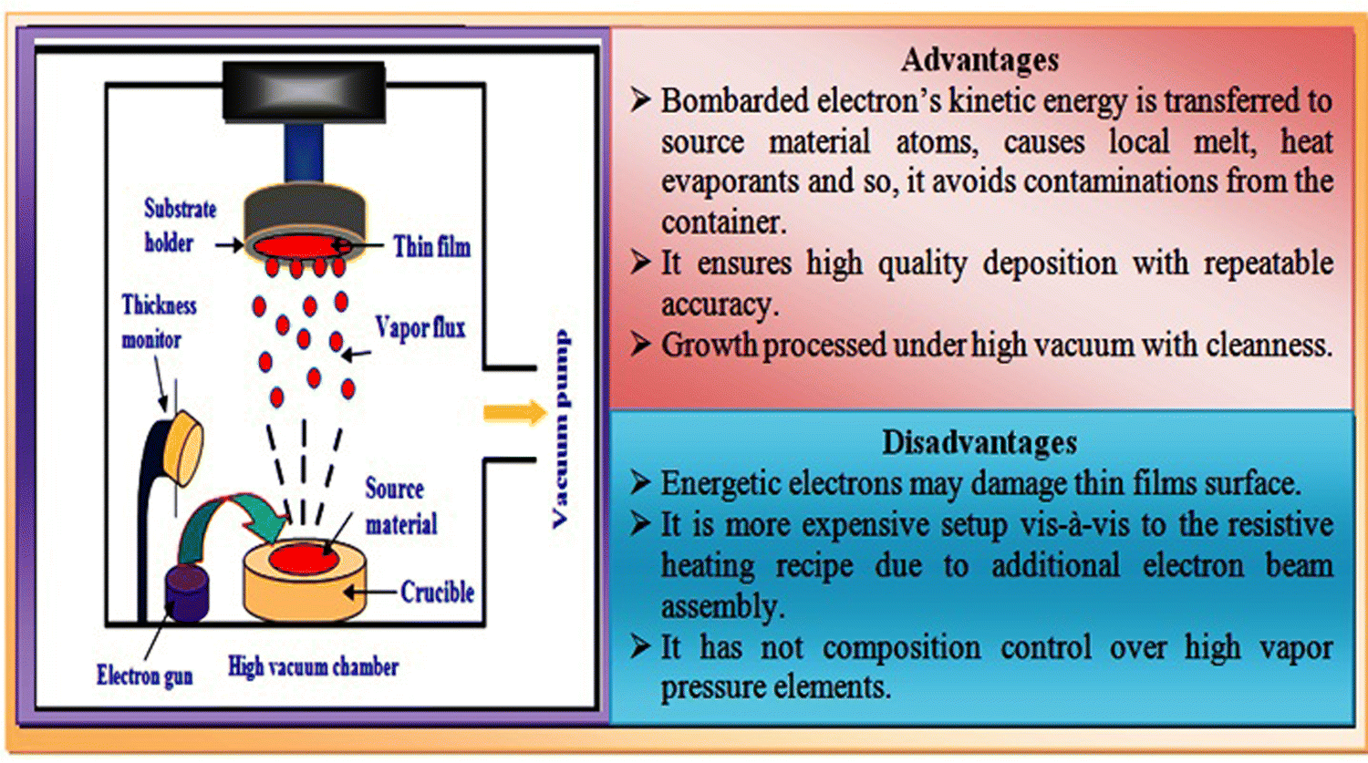 | ||
| Fig. 8 Overview of electron beam evaporation technique together with the advantages and disadvantages of this method. | ||
The electron beam evaporation technique is widely used due to its advantages including development of high-quality uniform thin films with repeatable accuracy, good stoichiometry and purity. To develop cost-effective layers, 400 nm thin ZnTe films were deposited by electron beam evaporation at the base vacuum of 1.5 × 10⁻⁶ Torr, which showed high quality and promising results.127 As stated, doping also alters the film quality and device performance, and accordingly vanadium-doped and undoped ZnTe thin film were prepared using the e-beam technique under vacuum of ∼8 × 10⁻⁶ Torr to explore impact of temperature on electrical properties.128 Electron beam-evaporated ZnTe thin films were used in photodiode sensor devices as a buffer layer with the architecture of p-ZnTe:N/CdTe:Mg/n-CdTe:I/GaAs.129 Employing this technique, ZnTe films were developed with a thickness of 200 nm and 300 nm at the base vacuum of ∼7.5 × 10⁻⁶ Torr as interface layers,82 thickness of 100 nm,84 300 nm130 and in the range of 100–500 nm131 at vacuum of 7.5 × 10⁻⁶ Torr as the back contact layers. The obtained film parameters employing this method are presented in Table 3 with the corresponding references.
| S. no. | Vacuum level (torr) | DR (Å s−1) | E g (eV), n | D (nm) | Phase and other(s) | Ref. |
|---|---|---|---|---|---|---|
| Where DR: deposition rate, n: refractive index, and ε: relative permittivity. | ||||||
| 1 | 7.5 × 10⁻⁶ | 8.5 | E g = 2.58–2.76 | 23–52 | Cubic | 181 |
| 2 | 6 × 10⁻⁷ | 8 | E g = 2.265 | 26 | Cubic, | 193 |
| n = 2.548 | ε = 8.6 × 10⁻³ lin−2 m−4 | |||||
| 3 | 6 × 10⁻⁶ | 2.05 | — | — | Amorphous, P-type | 128 |
| 4 | 2.2 × 10⁻⁴ | 3 | E g = 2.23 | 46–52 | Cubic | 113 |
| 5 | 10−5 | — | E g = 2.26 | 38–52 | Cubic | 28 |
| 6 | 1.50 × 10⁻⁶ | 4 | E g = 2.24 | ∼60 | Cubic | 127 |
However, despite its numerous merits, the electron beam technique suffers from the disadvantage of high vapour pressures depending on the source materials and ensuring the stoichiometry is also a challenging task. Thus to overcome these challenges, more specific technique such as molecular beam epitaxy can be employed, which offers the advantages of high purity and oxide-free deposition. According to these perspectives, in the next section, we present the molecular beam epitaxy (MBE) technique together with its role in device development.
2.3 Molecular beam epitaxy (MBE) technique
Molecular beam epitaxy (MBE) is the cleanest and most demanding technique utilized to grow thin films, which is performed under ultra-high vacuum (UHV) conditions and widely used to maintain the stoichiometry thus far. A pictorial view of the typical experimental setup together with its advantages and disadvantages is shown in Fig. 9. It consists of two or more Knudsen effusion cells (K-cells), located at bottom of a UHV chamber and aligned towards the center of the chamber, where the sample holder with substrates is positioned. Each K-cell is comprised of individual elements of interest in ultra-pure solid form, from which the desired film development occurs. The growth process is started by heating the K-cells corresponding to their melting point temperatures until the elements in each cell vapourise, following by reaching the substrates fixed at the holder, where the evaporants are deposited in accordance with the prevalent film growth mechanism, as stated earlier, and to achieve uniform growth, the substrates are continuously rotated at low rotation speeds with help of a stepper motor embedded with a magnetic manipulator.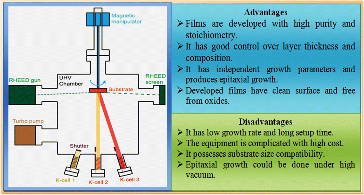 | ||
| Fig. 9 Overview of molecular beam epitaxy experimental setup together with its advantages and disadvantages. | ||
Thus, considering its merits, nitrogen-doped ZnTe thin films were developed employing the molecular beam epitaxy method by obtaining significant grain growth,132 and for their application in detectors and optoelectronic devices, the films were grown on GaAs substrates with better crystallinity.133 However, despite these merits, to employ this technique in deposition of thin films and devices associated with high crystallinity, it requires a longer processing time together with high vacuum compared to other techniques, and thus new options are necessary with certain merits. The following section presents the sputtering technique.
2.4 Sputtering deposition technique
Sputtering is a physical vapor deposition (PVD) technique and a physical route, which is classified based on the applied power source mainly as dc and rf sputtering, where the former uses a dc power supply, whereas the latter employs an rf supply with impedance matching. In this method, thin film deposition is undertaken by a speed transfer process, where the atoms or molecules of the desired material are expelled from a target through bombardment of high energy particles. Sputtered atoms are ejected from the target with a wide range of energies. The ejected atoms move towards the substrates, followed by condensation, and then high-quality thin film deposition in accordance with the merits of this technique. The experimental setup together with the advantages and disadvantages of the sputtering technique is shown in Fig. 10.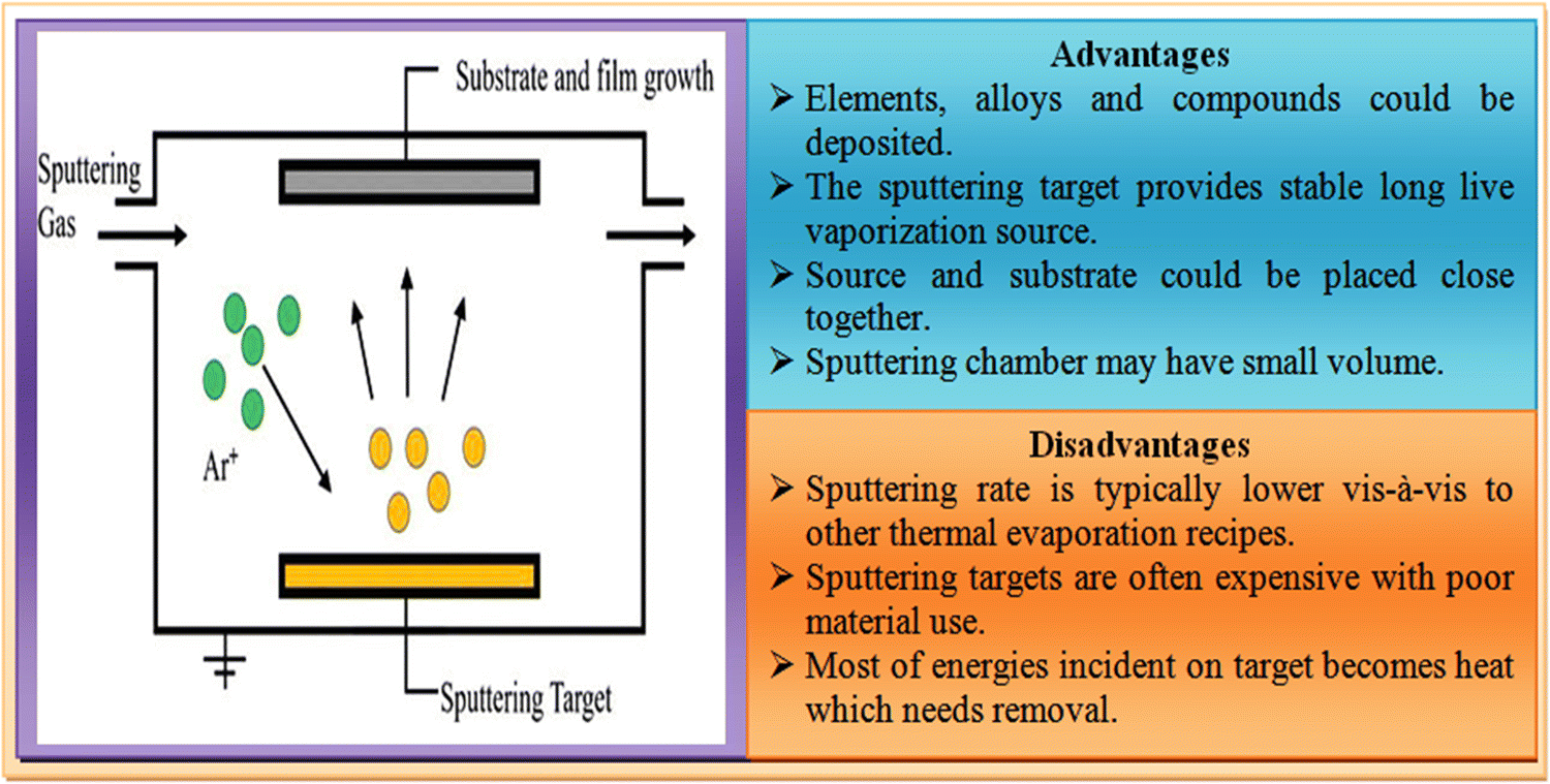 | ||
| Fig. 10 Pictorial view of the sputtering technique together with its advantages and disadvantages. | ||
Considering the advantages of the sputtering technique, ZnTe thin films were developed employing this method and the films exhibited high uniformity and homogeneity.134 For their application as a digital image filter, ∼2.4 μm films were deposited on GaSb and InAs substrates at the substrate temperature of 330 °C.135 For optoelectronic devices, 250 nm films were developed at different substrate temperatures using rf magnetron sputtering with a base vacuum of 1.1–1.2 × 10⁻² Torr.136 On applying sputtered ZnTe films as the back contact of CdTe solar cells, the devices demonstrated a significant improvement in stability and performance.137 These films were also deposited on a glass substrate with 50 W RF power and ∼1.5 × 10⁻⁶ Torr base vacuum.138 To develop intermediate band semiconductors, ZnTe:O films were deposited using this technique.139 The ZnTe:Cu thin films prepared were applied as back contacts in CdS/CdTe devices.140 The obtained relevant parameters for cubic-phase films using this technique are depicted in Table 4.
| S. no. | Vacuum level (torr) | Ref. gas | Optical parameters | D (nm) | Electrical parameter | Phase | Ref. | ||
|---|---|---|---|---|---|---|---|---|---|
| E g (eV) | n | ρ (Ω cm) | E a (eV) | ||||||
| 1 | 8.9 × 10⁻⁵ | Ar | 2.26 | 2.55 | 13 | — | 0.48 | Cubic | 93 |
| 2 | 1.2 × 10⁻² | N | 2.13–2.20 | 3–19 | 1.4× 10⁴–1.5 | — | Cubic | 136 | |
| 3 | 9.9 × 10⁻⁴ | Ar | — | — | — | — | — | Cubic | 137 |
| 4 | 1.33 × 10⁻⁵ | Ar | 2.31–2.26 | — | 27–50 | — | — | Cubic | 189 |
| 5 | 3 × 10⁻⁶ | Ar | 2.3–2.6 | — | — | — | — | Cubic | 139 |
However, the high cost of sputtering targets is the major drawback of this technique, which requires alternatives.
2.5 Electrodeposition technique
The electrodeposition method is a chemical route-based technique applied for the uniform coating of substrates or electrodes with a controlled film thickness, where electrochemical redox reactions occur on passing a current through an electrochemical cell comprised of the precursors of interest.141 This technique requires a low investment and enables production on a large scale with some limitations regarding the shape and size of the materials of interest.112 An outline of the electrodeposition experiment together with its advantages and disadvantages is shown in Fig. 11.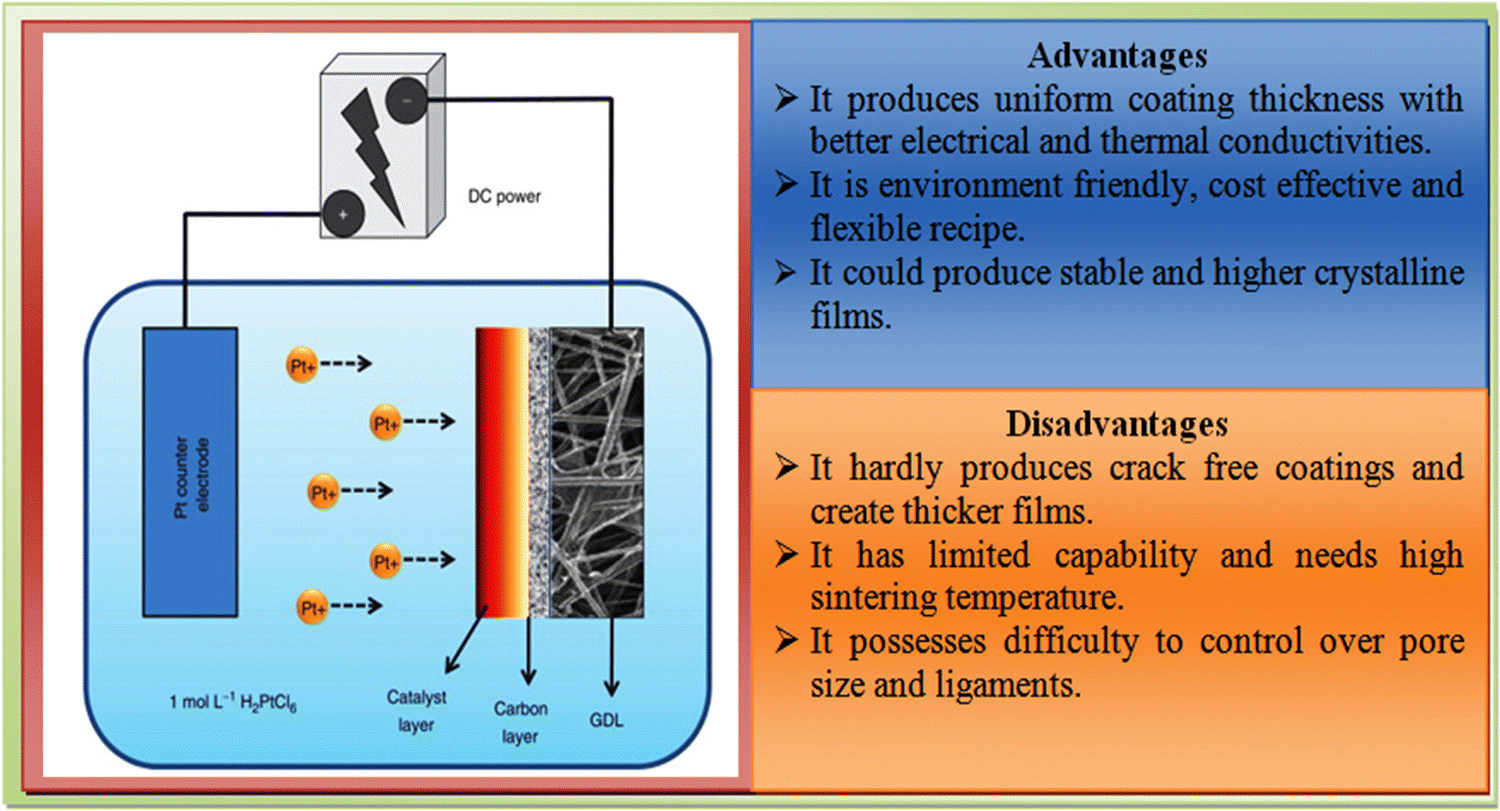 | ||
| Fig. 11 Overview of the electrodeposition experiment setup together with its advantages and disadvantages. | ||
Considering the merits and disadvantages of the electrodeposition technique, ZnTe films were grown on conductive oxide substrates for application in photoelectrochemical devices,142 optimized for electronic devices143 and evolved based on the electrodeposition temperature on FTO-coated glass substrates as the window layer in solar cell devices.144 For their application as a hetero-partner in solar cells, films were prepared followed by chloride activation with the architecture of glass/FTO/n-CdS/p-ZnTe/Au.145 Cu-doped and undoped ZnTe films were developed on metal substrates using this technique, where the obtained electrical properties were altered by the incorporation of a dopant.146
Considering the required technology, these films have also been developed thus far by employing laser evaporation, ion beam sputtering, laser chemical vapor deposition, plasma enhancement, chemical bath deposition, spray pyrolysis, liquid phase screen printing, pulsed laser deposition, spin coating and sol-gel techniques.147–156 The obtained film parameters are presented in Table 5 for electrodeposition together with the other chemical and physical route-based techniques such as SILAR, PLD and CSS.
| S. no. | Technique | pH/Pa (torr) | E g (eV) | D (nm) | ρ (Ω cm) | Phase | Ref. |
|---|---|---|---|---|---|---|---|
| Pa: deposition pressure, ρ: resistivity, Ea: activation energy, and ε: relative permittivity. | |||||||
| 1 | ED | (3.5 ± 0.1)–(5.5 ± 0.1) | 2.26 | 600 | — | Cubic | 142 |
| 2 | ED | — | 2.3–1.8 | — | — | Cubic | 144 |
| 3 | SILAR | 10.1 M | 2.75–3.15 | 75–270 | 107–108 | Cubic | 106 |
| 4 | PLD | 8 × 10⁻⁷ | — | 360–790 | — | — | 194 |
| 5 | ED | — | — | 140 | — | Hexagonal | 145 |
| 6 | CSS | 7.5 × 10⁻⁶ | 2.16–2.14 | 17–46 | 104–108 | Cubic | 195 |
Persistent efforts have been devoted thus far to insert ZnTe films as constituent layers to develop high-performance devices employing a variety of techniques, as detailed above, which are associated with some merits and drawbacks. Accordingly, resistive heating-based thermal evaporation is a widely used technique owing to its simplicity, easy operation, optimum material utilization, high purity thin film deposition and controlled deposition rate together with its availability in most laboratories across the globe given that it is mandatory for metal contact formation to the device. As stated, the film properties are also altered by doping with a suitable dopant to satisfy the device need. The developed thin film layers need to be optimized for the associated technology, which can be undertaken using the corresponding characterization tools. Thus, a brief outline of the doping and characterization is included in the following sections.
3. Impact of doping and post treatment on physical properties
The ZnTe is a p-type semiconducting material belonging to the II–VI group, which has attracted significant attention from the solar cell community due to its outstanding physical properties with direct optical energy band gap of 2.26 eV.157–162 It is mostly crystallized in a cubic crystalline structure similar to diamond, as shown in Fig. 5,102,163–171 and a leading material for a wide range of potential applications in solid-state electronic devices such as solar cells, green yellow light-emitting diodes, fluorescent screens, interference filters, laser diodes, solar panel displays, integrated circuits, terahertz radiation detectors, switching devices, gamma-ray detectors, nano-sensors, gas sensors, biomedical imaging devices, electroluminescent devices, electromagnetic field coatings, protective coatings, photodetectors, tandem solar cells, and quantum well structures.103,172–182Considering various applications, the discovery of new materials with advanced physical and chemical properties is highly required, and consequently the properties of materials need to be improved. Thus, to achieve better properties, ZnTe thin films can be doped, annealed, and treated after their deposition on various substrates. The optimization of physical properties such as structural, optical, photoluminescence (PL), electrical, topographical, morphological, and elemental properties of the single layers plays a significant role in device development with better performances. As stated, these properties can be analyzed using different characterization tools such as X-ray diffractometer (XRD), UV-vis spectrophotometer, PL spectrometer, source meter, atomic force microscope (AFM), scanning electron microscope (SEM), and energy dispersive spectroscope (EDS).183–192 The influence of different factors on the properties of ZnTe films is discussed in detail herein.
3.1 Structural properties
The structural properties of ZnTe thin films are typically investigated using X-ray diffraction (XRD). The evaluation of structural parameters such as crystal structure, inter-planar spacing, internal strain, crystallite size, dislocation density and number of crystallites per unit area of these films can be performed by analyzing their XRD patterns and using the corresponding relations available in the literature.82,84,102,123 The Scherrer and Williamson Hall relations are well-known approaches for the determination of the crystallite size, while the latter approach can also be used to simultaneously determine the strain as well. ZnTe thin films were deposited using various deposition techniques and it was observed that in most cases, ZnTe thin films were crystallized in the cubic phase with the zinc blende structure having the preferred (111) orientation, as depicted in Tables 2–5 depending on the different growth techniques. Sometimes, ZnTe films are also found to possess a hexagonal phase.143,189,193ZnTe thin films were employed for the development of devices with the architecture of ZnO/CdS/i-ZnTe/ZnTe:Cu/p-GaAs and to explore their viability considering their phase structure, the related research has been carried out thus far. The experimental studies suggest that annealing in an air atmosphere affects phase and structure of ZnTe thin films considerably, which may be owing to the mismatch in the thermal properties of the substrates and developed films and their imperfections including interstitials and vacancies. Accordingly, annealing at a suitable temperature is beneficial to prevent the formation of these imperfections, followed by improving the crystallinity and stoichiometry of the films.112,143,194 The annealing atmosphere also plays an important role in the modulation of the properties of films. ZnTe thin films were annealed under an argon atmosphere at temperatures of 200 °C, 300 °C, and 400 °C, where randomization in the texture of films occurred, which led to the growth of an additional preferred orientation at 400 °C, revealing to the evaporation of Te from the surface of the films.113 ZnTe thin films deposited at high substrate temperatures of 280 °C and 300 °C were found to be defect free with high carrier mobility and electrical conductivity188 but on increasing the substrate temperature further to 400 °C, a slight decrease in crystallinity was observed, which may be due to the re-evaporation of the Te-atoms.127
To improve the phase structure of ZnTe films, they have been doped with metals such as copper (Cu), silver (Ag), gadolinium (Gd), and vanadium (V). Copper- and silver-doped ZnTe films were found to be polycrystalline in nature, where their crystallite size decreased for the Ag-doped ZnTe samples and enhanced for the Cu-doped films due to the coalescence of smaller grains.121 The Cu-doped ZnTe thin films had a higher crystallite size in the range of ∼50 nm, as confirmed by Mahmood et al.195 Gd-doped ZnTe thin films have a polycrystalline nature with zinc blende cubic structure but their crystallite size was found to be reduced with an increase in Gd concentration due to the presence of defects involving the substitution of Gd ions and neighboring vacancies.120 Vanadium (V)-doped ZnTe thin films showed an amorphous nature, where metal doping led to an amorphous nature,128 while nickel doping did not change the properties of these films greatly.138 On depositing these thin films with varying angles through the thermal evaporation technique, XRD analysis confirmed that at lower angles, the films were Te rich, at moderate angles with a stoichiometric nature and Zn rich at higher angles.122 Hence, the structural properties of ZnTe films are affected by several factors, as discussed herein. Together with the phase structure, the optical properties also play great role in film quality and device performance. Thus, the following section is devoted to the optical properties of the ZnTe thin film layers.
3.2 Optical properties
The optical properties of ZnTe thin films such as optical absorbance, transmittance, refractive index (n), absorption coefficient (ε), and energy band gap (Eg) are investigated via ultraviolet-visible (UV-vis) spectroscopy, which is based on the interaction of light with matter. Their optical properties are typically influenced by the applied growth technique and doping together with pre- and post-treatments. Accordingly, they are affected by annealing, where the absorbance may increase or decrease after annealing the films, which depends on their crystallinity and grain growth. The interference fringes present in the transmittance spectra confirm the uniform deposition of these films.112 The pristine ZnTe thin film deposited by the thermal evaporation technique showed a band gap of ∼2.20 eV, which was lower than that of its bulk counterpart, which is ∼2.26 eV, where a slight reduction was observed for the films annealed at 200 °C be due to the combined effect of annealing inducing a change in the crystallite size and strain in the films.112 On annealing at 230 °C, they showed a sharp fall in transmittance at the band edge, which verified the good crystallinity of the films with a wide band gap of 2.29 eV.124 The pristine thin films showed a lower band gap of 1.9 eV compared to the annealed films (2.25 eV) at 350 °C, where excess unbound Te was absent for the annealed films.196The substrate temperature also affects the optical energy band gap of ZnTe thin films. Bacaksiz et al.113 developed ZnTe thin films at substrate temperatures of −123 °C and 27 °C followed by annealing at 200 °C, 300 °C, and 400 °C, where the band gap was elevated to be up to 2.23 eV with annealing and found to be in the vicinity of the standard value of 2.26 eV, while for substrate temperatures of 300 K and 373 K, it was observed at 2.24 eV and 1.95 eV, respectively. The interference patterns in the transmittance spectra confirmed the uniform deposition of these films.127 As stated, the optical energy band gap of ZnTe thin films is affected by the doped element too, and accordingly undoped ZnTe thin films possessed a band gap of 2.37 eV, while indium doping decreased it to 2.139 eV, which may be due to the change in the acceptor density.91 Vanadium doping decreased the band gap of ZnTe thin films owing to the decrease in activation energy.128 The incorporation of oxygen in ZnTe thin films resulted in a variation in band gap, where on increasing the oxygen concentration from 2% to 4%, it increased from 2.2 eV to 3.4 eV, which may be due to formation of oxides in the material.139 Cu- and Ag-doped ZnTe thin films had a lower transmittance and band gap compared to the undoped films, which was observed due to the formation of defects after doping. The reduction in band gap was attributed to the packing density, which may be due to the increase in crystallite size and decrease in grain boundaries. The band gap of the As-deposited, Cu-doped, and Ag-doped films was found to be 2.23 eV, 2.21 eV, and 2.19 eV, respectively.121 Similar work was reported for Cu-doped ZnTe thin films, where the transmittance and band gap were found to decrease due to the incorporation of Cu-atoms in the ZnTe lattice.195
The optical band gap and transmittance of ZnTe thin films also depend on their thickness, e.g., at a lower thickness of ∼564 nm, a higher band gap of 2.265 eV was obtained. Interference fringes were also observed, which indicated the good crystallinity of the deposited films.197 On depositing ZnTe thin films using the glancing angle deposition technique at different flux angles, the transmittance and band gap were found to increase due to the formation of porous structures as a result of shadowing and quantum confinement effects, respectively.198 However, when deposition was undertaken using the thermal evaporation technique, a high metallic Zn content was found in the thin films, resulting in a higher reflectance and lower transmittance.122 Hence, the optical properties of ZnTe films are greatly modified with pre- and post-deposition treatments. Together with the optical properties, the electrical properties are also correlated with the phase structure, which are affected by several factors, and thus the following section presents a detailed discussion on this.
3.3 Electrical properties
The electrical properties of the constituent layers play an important role, where typically for thin films, their conductivity and resistivity can be evaluated using a source meter, which provides current–voltage characteristics. In this case, ZnTe thin films are deposited on ITO, FTO and silicon substrates, where half of them is covered typically by aluminum foil to enable deposition only on half of the substrate, as shown in Fig. 12(a) for ITO substrates. Adhesive silver (Ag) paste is applied to form contacts on both the deposited film and uncoated ITO surface, as shown in Fig. 12(b), where thin copper (Cu) wires with negligible resistance are applied as probes.181 Besides, Hall measurement and photo-electrochemical cells are also employed to investigate the electrical properties. | ||
| Fig. 12 Illustration of (a) ZnTe thin film deposition on ITO substrate and (b) contact setup for the I–V measurement along the source meter interface. | ||
As stated, the electrical properties of ZnTe films were studied in terms of conductivity, resistivity, and semiconducting behavior, where these properties are affected by the deposition technique, doping and pre- and post-treatments. The conductivity of these films should be as high as possible for their application in solar cell devices.143 As stated, Hall measurements are also employed to investigate the electrical properties of ZnTe thin films.146 Using the electrodeposition technique, ZnTe thin films were deposited at different bath temperatures (30–90 °C), where with an increase in bath temperature, the conductivity was found to increase due to the filling of a separate set of traps lying below the Fermi level.196 Similarly, p- and n-type semiconducting layers were also prepared via the electrodeposition technique, followed by surface treatment employing CdCl2. The electrical conductivity obtained by photo-electrochemical cell (PEC) measurements demonstrated increased conductivity for p-type layers.145 Given that the conductivity is affected by doping, Mahmood et al.121 showed that ZnTe films with Cu- and Ag-dopant possessed increased conductivity. The Cu-doped films possessed higher conductivity compared to the Ag-doped thin films due to their improved crystal structure with few microstructural defects.120 The conductivity, carrier mobility, and concentration of ZnTe films were improved with Cu doping.146 Copper doping in ZnTe films resulted into enhanced charge carrier concentrations, which yielded improved conductivity in the films.195 The annealing atmosphere and conditions also affect the electrical properties, and accordingly annealing was performed under vacuum conditions and air atmosphere, where annealing in vacuum led to an increase in the conductivity of ZnTe thin films compared to the air-annealed films owing to the changes in their thermal properties by varying the residual gases and different interaction mechanisms with the film surface.84
Thus, the electrical properties of ZnTe films are significantly modified with pre- and post-deposition treatments. The surface morphology of the constituent layers of devices also affects film quality and device performance, and therefore, in the next section, we present details on the surface morphology of ZnTe thin films.
3.4 Surface morphology
Scanning electron microscopy (SEM) is used to study the surface morphology of ZnTe thin films, where detailed images can be captured by employing field-emission SEM (FESEM). The grain growth, grain size, shape and distribution could also be visualized by analyzing the SEM micrographs. The annealing of these films under different atmospheres, duration and temperature induces and modifies their micro-structural and morphological features. Olusola et al.143 deposited ZnTe films at a cathodic potential of 1600 mV, followed by annealing at 300 °C for 10 min in the air, where the SEM images showed uniformly covered films with varying grain sizes in the range of 127–509 nm due to the agglomeration of small grains.143 The annealing of ZnTe thin films resulted in a smooth surface with reduced intergranular spacing.196 The substrate temperature also enhanced the grain homogeneity and size due to the increase in the surface diffusion of atoms, which yielded films with voids and domes. The films deposited at substrate temperatures of −123 °C and 27 °C had a grain size in the range of 40–70 nm.113 The deposition conditions also altered the morphology of the films. The growth time not only led to an altered grain size but also smoother surface.134 On performing deposition using the GLAD technique, an increase in the deposition angle resulted in an enhanced tilting angle to the nanocolumns of the grown films.198 As the substrate temperature alters the morphology, ZnTe thin films with triangle-shaped pits were developed on a GaAs substrate with a substrate temperature of 530 °C using the MBE technique.133 Cu- and Ag-doped void-free ZnTe thin films with a smoother surface were developed, where the Cu-doped thin films showed a higher grain size compared to that of the Ag-doped and undoped ZnTe thin films.121 Undoped and Cu-doped ZnTe thin films were developed, where the Cu-doped ZnTe thin films possessed obvious grains and grain boundaries due to the reduction in agglomeration.195 ZnTe:N thin films were grown at different substrate temperatures using the MBE technique, which consisted of mirror-like compact grains.132 Findings suggested that doping and annealing significantly enhance the surface morphology of these thin films. Together with the morphology, the elemental composition and stoichiometry of the films also influence their quality and device performance, and thus, in the next section we discuss the compositional properties.3.5 Compositional properties and stoichiometry
The composition of materials can be explored by both elemental dispersive spectroscopy (EDS) and X-ray photoemission spectroscopy (XPS), where EDS is a significant non-destructive X-ray technique and typically used to determine the compositional/elemental properties of powders and films. For the optimum utilization of the source, generally the EDS is coupled with SEM instrumentation, which also makes it cost effective. Considering the target domain, the relevant findings are discussed herein, where a change in composition changes the nature of the films from p- to n-type and vice versa. The cathodic potential used during the deposition of ZnTe films influences the weight percentage of Zn and Te elements, and accordingly ZnTe thin films were developed with cathodic potentials of 1500 mV and 1700 mV,143 where the compositional analysis demonstrated the formation of p-type films with Te richness at a lower cathodic potential and higher cathodic potential resulted in n-type behavior with excess Zn. The thickness evolution showed a decrease in Zn/Te ratio with an increase in ZnTe film thickness.134 On growing films with positive and negative potential using the electrodeposition technique, the films exhibited richness in Te and Zn elements, respectively.196 The substrate temperature also affected the weight percentage of Zn and Te elements in these films and the films deposited on glass substrates at different substrate temperatures of 100 °C, 200 °C, and 400 °C possessed Zn:Te atomic compositions of 54:45, 51:48, and 52:47, respectively, where among them, the findings demonstrated better stoichiometry of the films deposited at a substrate temperature of 200 °C.127 The deposition angle also alters the stoichiometry of the developed constituent layers, and accordingly, ZnTe films were deposited at different angles of 0°, 20°, 40°, 60°, and 80° employing the thermal evaporation technique, which demonstrated Te richness at lower deposition angles and Zn richness at higher angles. This could be explained based on the kinetic theory of gases or the collisions occurring between the Zn atoms and Te2 molecules during evaporation.122 Hence, as deliberated, a number of factors play an important role in controlling the composition and stoichiometry of ZnTe films. The surface topography and roughness also affect the constituent layers of the devices, and thus, in the next section, this is discussed.
3.6 Surface topographical properties and roughness
The surface topography of thin films can be evaluated by atomic force microscopy (AFM), which is also known as scanning probe microscopy and generates images of samples with the desired resolution in accordance with the users need and limitations of the instrumentation. AFM analysis provides details on the topography of semiconducting materials at the angstrom scale together with surface roughness and quantitative measurements on grain size, step heights, etc. Additionally, advanced AFM measurements enable qualitative mapping regarding various properties and parameters such as adhesion, modulus, dopant distribution, conductivity, surface potential, electric field, and magnetic domains. AFM measurements are undertaken through three modes, i.e., contact, semi-contact and non-contact modes, based on the instrumentation, where equipment is manufactured with one of these modes.Herein, in accordance with the device architecture or individual constituent layers, the relevant literature available thus far is analysed. The surface roughness of ZnTe thin films was found to decrease with annealing, resulting in the formation of uniform films with enhanced grain size or grain growth, where their 3D images showed columnar growth patterns.143 Indium doping in ZnTe films resulted into better crystallinity and surface topography.119 As stated, the substrate temperature affects the surface properties of these films, and accordingly the 3D surface profiles of these films exhibited grainy and polycrystalline topographies, which were fabricated at a substrate temperature of 100 °C and showed a high domain size with better root mean square of ∼8 nm compared to the films fabricated at other substrate temperatures, i.e., 27 °C, 200 °C and 400 °C.127 The topography of the ZnTe films with a thickness in the range of 120–600 nm thickness was revealed to exhibit an increased average roughness from 6.7 nm to 33.7 nm and root mean square (RMS) roughness from 8.27 nm to 44.2 nm.124 For MBE grown ZnTe:N thin films, the surface root mean square roughness was found to increase with growth temperature.132 Hence, surface topographies and statistical parameters of films were greatly influenced by the different pre- and post-treatments as well as the deposition conditions. The individual thin film layers optimized through these tools are employed for the development of devices, and based on the available literature thus far, they are discussed in the followed section together with the relevant science and importance of the present review domain.
4. Critical insights into the role of ZnTe layers in CdTe thin film solar cells
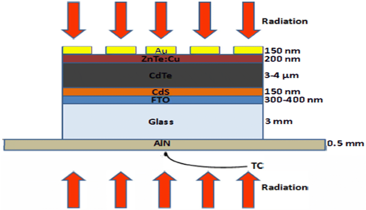
The research on CdTe thin film solar cells has been predominantly undertaken in the last five decades, where a strong improvement in efficiency has been achieved in the last decade. In 1972, the first CdTe thin film solar cell was introduced by Bonnet and Rabenhorst with a PCE of 6%.199 Typical CdTe thin film solar cell devices consist of different layered structures, where the superstrate architecture is comprised of glass/TCO/window/absorber/interface/metal contact, as shown in Fig. 13, where a ZnTe layer is employed as an interface.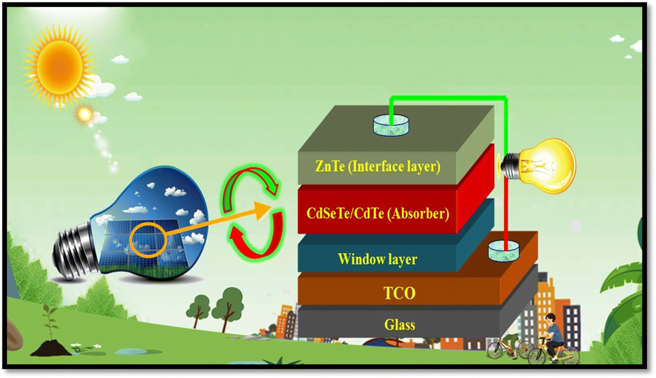 | ||
| Fig. 13 Pictorial view of ZnTe back contact comprised of CdSeTe/CdTe thin film solar cell device structure together with natural conditions. | ||
The transparent conducting oxides (TCOs) are highly degenerative semiconductors, which possess high band gap. Fluorine-doped tin oxide (FTO) and indium-doped tin oxide (ITO) are well known TCO materials, which are employed thus far to develop CdTe devices with the superstrate device structure. To transmit the maximum incident irradiance and develop a heterojunction, a window layer of thickness in the range of 60–100 nm is applied. CdS has a wide band gap of 2.4 eV with n-type nature and is typically used as the window layer in CdTe devices to achieve high efficiency but nowadays magnesium-doped zinc oxide (MZO) has been found to be more transparent and appropriate alternative to the CdS window layer to attain higher power conversion efficiency, together with environmental aspects. To harvest the maximum incident solar irradiance, a CdTe absorber layer having a thickness of 3–5 μm is employed, which has the optical energy band gap of 1.45 eV with p-type conductivity and assures almost complete absorption. The net carrier concentration and lifetime are affected by the crystal structure of the absorber layer, which considerably leads to a change in both the open-circuit voltage (Voc) and short circuit current density (Jsc). In recent years, a higher power conversion efficiency has been attained with enhanced Jsc by introducing a lower band gap CdSeTe supporting absorber as an interface and replacing CdS with a more transparent and wider band gap material, i.e., MgxZn1−xO (MZO).64,66,67 As stated, MZO is a promising alternative to replace the CdS window layer in CdTe-based solar cells and its electron density can be tuned, which provides flexibility in controlling the conduction band offset together with the recombination rates at the TCO/MZO and MZO/Cd(Se)Te interfaces, where the CdTe absorber layer is engineered by employing graded band gap Se (Selenium) insertion to the latter interface.59,70 The ZnTe semiconducting layer acts as an interface layer between the CdTe absorber and rear-metal contact, which limits the recombination losses dealing with minority carriers due to its captivating performance. To complete the device structure, metal contacts are developed using gold (Au), silver (Ag), copper (Cu) and platinum (Pt) employing the resistive heating-based thermal evaporation technique, but due to high melting point of the Pt leads to radiative heat and its high cost reduce applicability. In the CdTe-based device with a superstrate architecture, this rear metal contact has the task of collecting the charge carriers at the absorber side by contacting the device with an external circuit.200–207 To date, CdTe solar cell devices with the architecture of glass/MZO/CdSeTe/CdTe/ZnTe/metal contact have demonstrated the maximum power conversion efficiency (PCE) of 22.1%.32,69,208 CdTe devices with the configuration of glass/FTO/CdS/CdTe/CdCl2/ZnTe:Cu/Au demonstrated a PCE of 11.25%, where Cu-doped ZnTe was applied as the back contact. Herein, the CdTe absorber was chloride activated at 360 °C, 380 °C, and 400 °C, where the best performance was attained at 380 °C.75
Although the CdTe semiconducting material is a promising absorber material for thin-film solar cell devices, the maximum achieved open circuit voltage (Voc) for these devices is still lower than the theoretically predicated Voc due to the barriers developed at the back contact. A simple CdTe device with the configuration of glass/FTO/CdS/CdTe/ZnTe:Cu/Au, as shown in Fig. 14, was developed with copper-doped ZnTe as the back contact layer. To control the Cu distribution together with ZnTe:Cu film activation, annealing was performed, where annealing for 30 s at 320 °C improved the fill factor and open circuit voltage, attaining a PCE of 14.5% under the optimal conditions without compromising the short circuit current.209
 | ||
| Fig. 14 CdTe solar cell device configuration by employing ZnTe:Cu as the back contact. Reprinted with permission from ref. 209. Copyright (2014) IEEE publications. | ||
A single-crystal CdTe solar cell device was developed on GaAs substrates by employing metal–organic chemical vapor deposition, where a highly conducting arsenic-doped ZnTe layer was grown on GaAs substrates to act as a buffer layer to the CdTe absorber. The hole concentration in CdTe increased with an increase in VI/II ratio under a high arsenic concentration during the growth mechanism. The electrical findings demonstrated the Ohmic behavior of the CdTe/ZnTe and ZnTe/GaAs contacts. Although the performance in terms of Voc of 0.63 V and PCE of 4.5% was found to be low, it could be enhanced by decreasing the dislocation density associated with the CdTe thin film layers.210
Although persistent efforts have been devoted by researchers thus far to overcome the limitations of the back contact by employing Cu doping, which can form effective back contacts, the presence of Cu in the CdTe absorber also creates the detrimental recombination centers. In contrast, an effective approach to reduce the back contact barriers in these devices was to introduce a ZnTe:Cu buffer layer with glass/FTO/SnO2/CdS/CdTe/(CdCl2)/ZnTe:Cu/Au architecture, where both the FF of 73.7% and Voc of 0.85 V were improved, while the current density of 24.3 mA cm−2 and PCE of 15.3% remained unchanged, which may be attributed to the passivation of recombination related to defects in the back contact region. The quantitative analysis showed the segregation of the majority of Cu in the Au metallization layer and a ZnTe buffer appeared to inhibit Cu diffusion in CdTe.211 The relevant energy band diagram is shown in Fig. 15(a and b), where a negligible valence band offset of ∼0.1 eV was attained at the CdTe/ZnTe interface but a significant Schottky barrier was present at the ZnTe/Au interface. After Cu doping, the ZnTe:Cu thin film layers became more p-type due to the activation of the Cu dopant, which shifted the valence band offset into a position that reduced barrier to hole transport at the CdTe/ZnTe interface.211
 | ||
| Fig. 15 Energy band diagrams of CdTe devices with (a) undoped and (b) Cu-doped ZnTe back contact. Reprinted with permission from ref. 211. Copyright (2015), Elsevier Publications. | ||
The superstrate architecture devices are finished by the formation of a metal contact on the developed stack of the device, where the metal material also impacts the device performance, and accordingly metal contact material evolution is undertaken with the device configuration of glass/ITO/CdS/CdTe/CdCl2/ZnTe/Cu/metal contact where ZnTe is applied as the back contact followed by rf sputtered Cu layer, and then Au, Cr and Ti are applied as metal contacts. The developed devices demonstrated almost similar performances with the maximum PCE of 14.5% for the Au contact.212 As stated, strong progress in the power conversion efficiency of CdTe solar cells has been recorded for devices with an MZO optical window instead of the conventional CdS by introducing a CdSeTe supporting absorber together with CdTe by modifying the architecture,64,66,67 causing the highest PCE of 22.1%.32,69,70 Efforts have also been made to overcome the back contact issues by doping the ZnTe layer with copper to enhance its performance and thickness evolution of ZnTe, where Cu deposited via the rf sputtering route at 200 °C substrate temperature with the device structure of glass/FTO/ZnO/CdTe/ZnTe:Cu/Au. The findings demonstrated a PCE of 15.6% for 80 nm ZnTe and 7 nm Cu.213
The absorbance in the conventional device architecture of glass/FTO/CdS/CdTe/metal contact at a shorter wavelength is considerably limited by the CdS optical window, where on replacing it by MZO, new insights were revealed. However, the replacement of CdS with magnesium zinc oxide (MZO) resulted in a weak built-in potential at the MZO/CdTe heterojunction and insufficient driving force to repel the photo-generated carriers. Thus, to mitigate this problem, a CdS layer was incorporated between MZO and CdTe based on the architecture of glass/FTO/MZO/CdS/CdSe/CdTe/ZnTe:Cu/Au, and consequently, the built-in potential was improved from 0.369 V to 0.579 V together with an enhanced fill factor, open circuit voltage and quantum efficiency (QE) response.214 The CdTe device with the structure ITO/ZnO/CdSe/CdTe/ZnTe:Cu/Au is shown in Fig. 16(a) together with the energy band diagram using a 20 nm ZnTe:Cu back contact annealed at 200 °C, and the device yielded a PCE of 6.38%.215
 | ||
| Fig. 16 (a) CdSe and ZnTe:Cu back contact-comprised CdTe device with (b) energy band diagram. Reprinted with permission from ref. 215. Copyright (2019), MDPI Publications. | ||
Given that a low resistive back contact is needed to fabricate high-efficiency devices, to well match the interfacial properties of ZnTe, a heavily doped p-type Cu1.4Te, ZnTe/Cu1.4Te alloyed bilayer was synthesized for application in a device with the architecture of glass/FTO/SnO2/CdS/CdTe/ZnTe/Cu1.4Te/Au, as shown in Fig. 17 with its energy band diagram. This lower Schottky barrier and lesser carrier recombination ZnTe/Cu1.4Te-containing device demonstrated a PCE of 15% due to the improved adaption to band bending.216
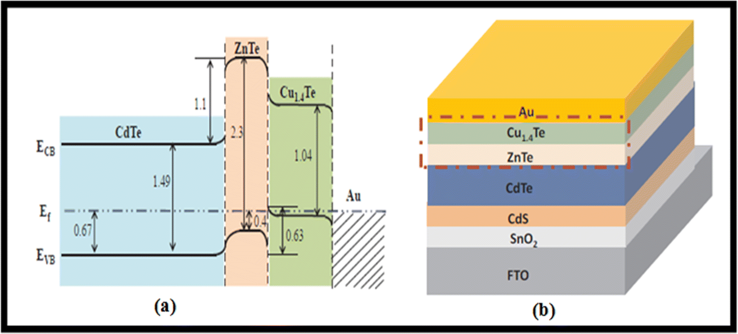 | ||
| Fig. 17 ZnTe/Cu1.4Te-containing glass/FTO/SnO2/CdS/CdTe/ZnTe/Cu1.4Te/Au architecture CdTe device with (a) energy band diagram and (b) device stack. Reprinted with permission from ref. 216. Copyright (2019), Elsevier Publications. | ||
Arsenic-doped ZnTe layers demonstrated higher conductivity compared to the undoped ZnTe, where on applying a heavily doped p-type 100 nm ZnTe:As back contact with the device architecture of glass/ITO/Cd1−xZnxS/CdTe-CdCl2/ZnTe:As/CdS/CdCl2/Au and annealed stack up to ZnTe:As at 420 °C in a hydrogen atmosphere, a significantly enhanced Voc and PCE 11.9% were achieved.217 To reduce the back contact barrier, ZnTe:Cu was applied with the device architecture of glass/FTO/SnO2/n-CdS/p-CdTe/ZnTe:Cu/Au, and it was revealed that the reaction at the CdTe/ZnTe:Cu interface during the heat treatment process could modify the interfacial band alignment, which reduced the defect-associated recombination and supported the transport of holes, resulting in a PCE of 15.8%.218 The deposition time and temperature to the ZnTe back contact alter the performance, and accordingly a device was developed with the configuration of glass/FTO/CdS/CdTe/ZnTe/Cu/Au, as depicted in Fig. 18, together with the relevant junction creation mechanism, where ZnTe was deposited at 700 °C for 3 min. The developed device demonstrated a PCE of 12.2%.219
 | ||
| Fig. 18 CdTe solar cell device with architecture of (a) glass/FTO/CdS/CdTe/ZnTe/Cu/Au and (b) pictorial illustration of the junction development mechanism. Reprinted with permission from ref. 219. Copyright (2021), AIP Publications. | ||
A CdTe device with the architecture of glass/FTO/SnO2/CdS/CdTe/CdCl2/ZnTe:Cu/Mo was developed by employing ZnTe:Cu as the back contact, where a Cu layer was sputtered over ZnTe to improve the charge collection and the devices demonstrated a PCE of 14.3%, which was identical for the 10 nm and 2.5 nm Cu samples annealed at 450 °C and 420 °C, respectively.220 As stated, the MZO and CdSeTe devices performed better, and accordingly, devices were developed with the architecture of glass/FTO/MZO/CdSeTe/CdTe/ZnTe/Te/C/Ni, as depicted in Fig. 19. The devices developed with a 100 nm ZnTe back contact annealed at 350 °C for 15 min in an air atmosphere revealed a significant improvement in open circuit voltage, attaining a PCE of 12.96%. In these devices, carbon followed by nickel paint worked as the rear contact, where ZnTe was also followed by a Te layer.221
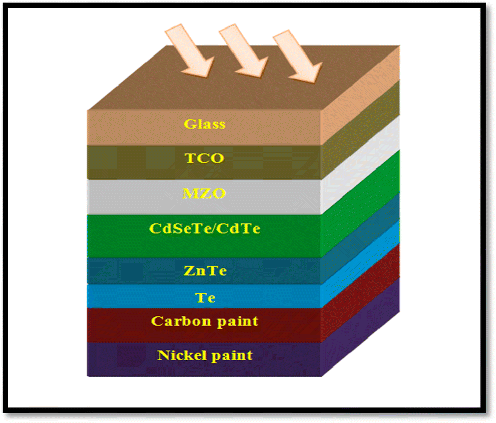 | ||
| Fig. 19 ZnTe/Te-comprised CdTe device where C/Ni is applied as the rear contact. Reprinted with permission from ref. 221. Copyright (2018), IEEE Publications. | ||
To improve the charge collection in CdTe solar cells in a longer wavelength region, co-evaporated CdSexTe1−x layers were employed with the FTO/CdS/CdSeTe/CdTe/ZnTe:Cu/Au structure, where ∼3.5 μm CdTe absorber was deposited by close-spaced sublimation with 70 nm 6% Cu-doped ZnTe via the thermal evaporation technique, where the optimal band gap of ∼1.40 eV of support the CdSeTe absorber resulted in an enhanced PCE of 16.2%.222 The performance parameters of CdTe devices developed thus far with a ZnTe back contact are presented in Table 6.
| Device architecture (s) | V oc (V) | J sc (mA cm−2) | FF (%) | η (%) | Ref. |
|---|---|---|---|---|---|
| Glass/FTO/CdS/CdTe/CdCl2/ZnTe:Cu/Au | 0.72 | 21.99 | 70.32 | 11.25 | 137 |
| Glass/FTO/CdS/CdTe/ZnTe:Cu/Au | 0.82 | 24.3 | 71.1 | 14.5 | 209 |
| CdTe/ZnTe-based device | 0.63 | 16.8 | 43 | 4.5 | 210 |
| Glass/FTO/SnO2/CdS/CdTe/CdCl2/ZnTe:Cu/Au | 0.85 | 24.3 | 73.7 | 15.3 | 211 |
| Glass/FTO/ZnO/CdTe/ZnTe:Cu/Au | 0.83 | 26.3 | 71 | 15.6 | 213 |
| Glass/ITO/ZnO/CdSe/CdTe/ZnTe:Cu/Au | 0.65 | 19.73 | 49.75 | 6.38 | 215 |
| Glass/FTO/SnO2/CdS/CdTe/ZnTe/Cu1.4Te/Au | 0.81 | — | 73 | 15 | 216 |
| Glass/ITO/Cd1−xZnxS/CdTe/CdCl2/ZnTe:As/CdS/CdCl2/Au | 0.69 | 23.7 | 72 | 11.9 | 217 |
| Glass/FTO/SnO2/n-CdS/p-CdTe/ZnTe:Cu/Au | 0.83 | 25.6 | 74.1 | 15.8 | 218 |
| Glass/FTO/CdS/CdTe/ZnTe/Cu/Au | 0.74 | 41.6 | 39 | 12.2 | 219 |
| Glass/FTO/MZO/CdSeTe/CdTe/Te/metal contact | 0.77 | 26.6 | 62.9 | 12.96 | 221 |
| FTO/CdS/CdSeTe/CdTe/ZnTe:Cu/Au | 0.82 | 28.8 | 68.7 | 16.2 | 222 |
| Glass/FTO/MZO/CdSeTe/CdTe/ZnTe/metal contact | 0.88 | 31.7 | 78.5 | 22.1 | 70 |
An overview of the CdTe solar cell history with the role of the ZnTe back contact is depicted graphically in Fig. 20.
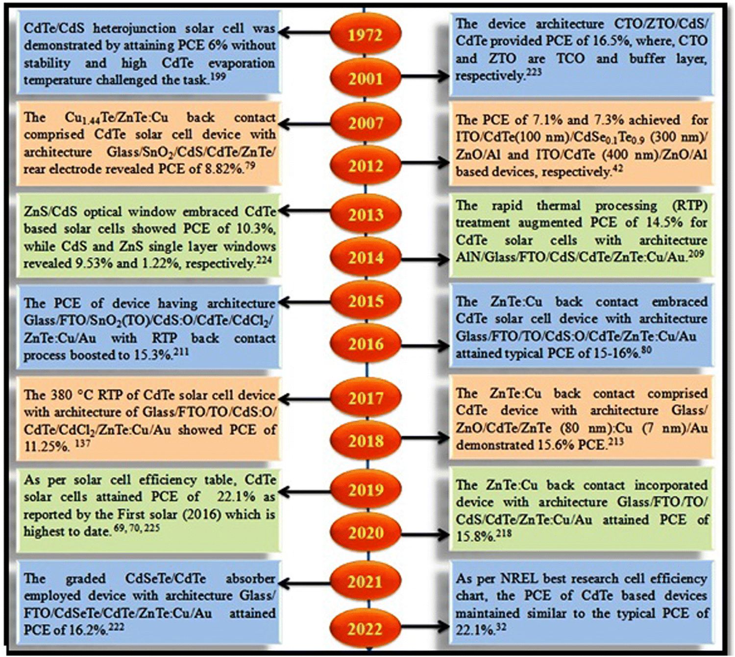 | ||
| Fig. 20 An overview of the history of ZnTe back contact-comprised CdTe thin film solar cells.32,42,69,70,79,80,137,199,209,211,213,218,222–225 | ||
The device design also plays an important role in the development of high-performance devices, and accordingly the following text is devoted to the simulation modeling for designing devices comprised of ZnTe as the back contact layer together with its merits and drawbacks.
A theoretical analysis of CdTe solar cell devices was undertaken using microelectronic and photonic structures to examine their performance parameters, i.e., Voc, Jsc, FF, and PCE, where simulations were done by varying the CdTe absorber layer thickness by predicting that a 1 μm thick layer was sufficient to get the desired efficiency, and here, the absorber was followed by a 100 nm ZnTe back contact layer to minimize the recombination losses and barrier height, with the device configuration of glass/SnO2/Zn2SnO4/CdS/CdTe/ZnTe/Ni, and a PCE of 22.53% was attained.226 Although simulation was performed employing the device architecture of ZnO/CdS/ZnTe/metal-contact, where the ZnTe layer acts as the absorber, CdS as the buffer and ZnO as the optical window employing the solar cell capacitance simulator (SCAPS) code and PCE of 10% attained, the incorporation of grain boundaries is still unclear and the applied absorber is not suitable, and thus simulation still cannot give a clear picture on the optimal device design.227
Employing the SCAPS-1D code, a ZnTe:Mo back contact-comprised CdTe device was designed based on the configuration of glass/TCO/ZnO/CdS/CdTe/ZnTe:Mo/metal contact, which predicted a Voc of 0.925 V and PCE of 19.06%.228 Although the SCAPS 1D code has been employed, it does not consider the impact of the grain boundaries in the constituent layers, and therefore the exact mechanism is still unknown, which significantly affects the device performance. The prevalent CdCl2 treatment and Cu doping of the CdTe absorber were replaced by arsenic (As) to develop a Cu-free back contact, as shown in Fig. 21, with a predicted PCE of 20.8%.68
 | ||
| Fig. 21 CdSeTe/CdTe device design with ZnTe back contact employing simulation modeling. Reprinted with permission from ref. 68. Copyright (2019), ACS Publications. | ||
A device was also designed with the architecture of glass/TCO/window layer/CdSeTe/CdTe/ZnTe/back contact, where magnesium-doped zinc oxide (MZO) was employed as the optical window and CdSeTe/CdTe as the absorber layer with the ZnTe interface. The simulation-based photovoltaic parameters of the CdTe device designs having ZnTe back contact layers are presented in Table 7.
| Device architecture (s) | V oc (V) | J sc (mA cm−2) | FF (%) | η (%) | Ref. |
|---|---|---|---|---|---|
| Glass/SnO2/Zn2SnO4/CdS/CdTe/ZnTe/Ni | 1.06 | 24.28 | 87.5 | 22.53 | 226 |
| Glass/ZnO/CdS/ZnTe/metal contact | 1.81 | 7.01 | 78.84 | 10 | 227 |
| Glass/TCO/ZnO/CdS/CdTe/ZnTe:Mo/metal contact | 0.93 | 26.87 | 76.7 | 19.06 | 228 |
| Glass/TCO/buffer layer/CdSeTe/CdTe/ZnTe/back contact | 0.86 | 30.5 | 79.8 | 20.8 | 68 |
As stated, thin film solar cells are comprised of several thin film constituent layers, which contain huge grain boundaries, i.e., two-dimensional defects that act as trap states and recombination centers to the generated and flowed charge carriers. The parallel and perpendicular alignment of these grain boundaries affects the charge carrier flow; however, the simulation codes reported to date do not consider the impact of grain boundaries on the device performance. Thus, the predictions employing simulation codes cannot be applied efficiently in the development of real devices.39 The power conversion efficiency of single-junction solar cell devices is limited by the Shockley Queisser limit based on the principle of detailed balance, which could be surpassed by a tandem device, where a narrower absorber band gap sub-cell is stacked by a wider band gap sub-cell to harvest the maximum incident solar irradiance, where light comes from the wider band gap sub-cell side. For tandem devices, the highest recorded PCE 47.1% was reported by NREL, USA for six junction III–V tandems with 143 sun direct incidence AM1.5D,229 while there is still room for the development of CdTe-based tandems, where the ZnTe back contact embraced CdTe device can be employed as the top sub-cell with perovskite or silicon based bottom sub-cell. The pictorial views of the perovskite/CdTe and c-Si/CdTe tandem architectures are depicted in Fig. 22, which can be employed, but the development of CdTe-based tandem devices is a challenging task for the research community.
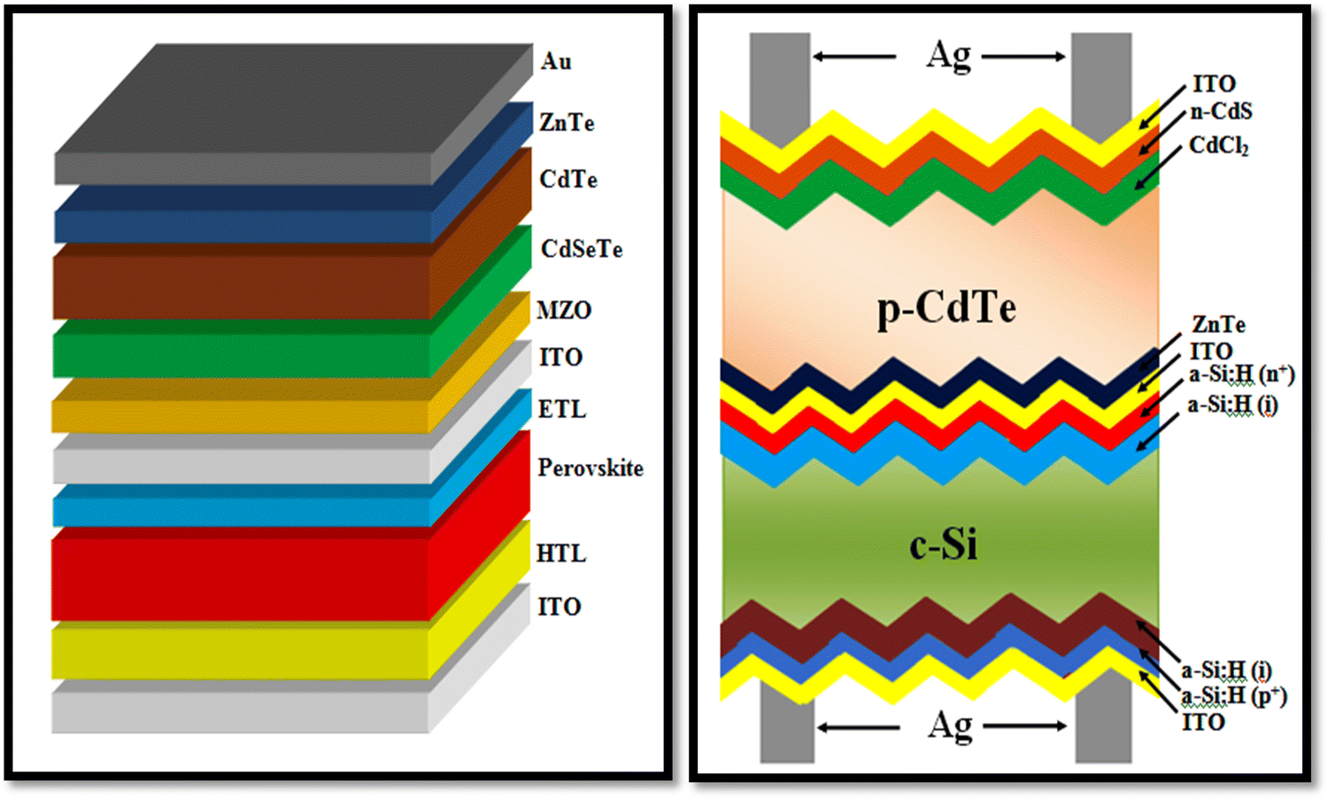 | ||
| Fig. 22 Graphical illustration of anticipated perovskite/CdTe and Si/CdTe tandem designs, where the CdTe device is suggested as the top sub-cell and perovskite and silicon devices as bottom sub-cells to harvest maximum incident irradiance. | ||
5. Challenges and opportunities
CdTe thin film solar cells have potential to significantly contribute to meeting the global energy demand by providing a cost-effective road map. Their constituent layers also play a vital role in the optimization of the devices, where in CdTe devices, a ZnTe back contact can reduce the parasitic resistance, while enhancing their performance. In the present review, we concisely discussed the role of the ZnTe back contact in the enhancement of the performances of CdTe thin film solar cells. We also included an overview of the CdTe device development history by incorporating ZnTe back contacts, where the development strategies to produce the ZnTe thin film layers together with the characterization findings thus far were comprehensively discussed including phase structure, optical constants, morphology and topography of the ZnTe single layers to determine their viability in demonstrating better-performance devices. The merits and drawbacks of the development strategies were also presented according to the evolution of materials in terms of doping. The insertion of a ZnTe back contact between the CdTe absorber and metal contact reduces the electron losses by enhancing the open circuit voltage and device performance, which is demonstrated to be important in the modern era of cutting edge energy-driven technology and rivals the evergreen and champion silicon solar cell technology based on a few aspects. Parallel device design work employing simulation modeling has also been reported but still needs experimental validation. The introduction of an MZO optical window and CdSeTe supporting absorber also significantly enhanced the device performance, which opens the applicability of these devices in the tandem architecture as top sub-cells with perovskite and silicon as bottom sub-cells. The simulation modeling codes developed to date do not consider the impact of the grain boundaries on the devices, which is a major roadblock to get device design support in real device development. Considering the findings and obstacles in the development of high-performance devices to cater the present energy needs of society, suitable simulation modeling codes for the design of devices are required comprised of the impact of grain boundaries together with significant work on CdTe-based tandems. Although we attempted to include all the relevant literature dealing with the ZnTe back contact in CdTe devices reported thus far, we apologize if any findings were inadvertently omitted.Competing interests
The authors declare that they have no known competing financial interests or personal relationships that could have appeared to influence this review.Data availability
All the data presented in the review manuscript are extracted from already published articles as listed in reference section.Author contributions
Deepak Suthar: writing – original draft. Sakshi Chuhadiya: writing – original draft. Ritika Sharma: writing – original draft. Himanshu: writing – original draft. M. S. Dhaka: conceptualization, supervision, writing – original draft.Conflicts of interest
The authors declared that they have no conflict of interest.Acknowledgements
The authors are thankful to Department of Science and Technology, Government of Rajasthan, Jaipur for providing financial support through Research and Development Project Vide file no. F.7(3) ST/R and D/2016/5677 and to the Ministry of Education, Government of India and Ministry of Higher Education, Government of Rajasthan for Research and Innovation project under RUSA 2.0 scheme.References
- S. Sinha, D. K. Nandi, S. H. Kim and J. Heo, Sol. Energy Mater. Sol. Cells, 2018, 176, 49–68 CrossRef CAS.
- I. Dincer, Energy Sources, 2001, 23, 83–92 CrossRef CAS.
- I. Dincer, Sustain. Energy Rev., 2000, 4, 157–175 CrossRef.
- R. Gross, M. Leach and A. Bauen, Environ. Int., 2003, 29, 105–122 CrossRef PubMed.
- A. Harjanne and J. M. Korhonen, Energy Policy, 2019, 127, 330–340 CrossRef.
- M. Shao, Z. Han, J. Sun, C. Xiao, S. Zhang and Y. Zhao, Renewable Energy, 2020, 157, 377–403 CrossRef.
- N. L. Panwar, S. C. Kaushik and S. Kothari, Renewable Sustainable Energy Rev., 2011, 15, 1513–1524 CrossRef.
- M. K. H. Rabaia, M. A. Abdelkareem, E. T. Sayed, K. Elsaid, K. J. Chae, T. Wilberforce and A. G. Olabi, Sci. Total Environ., 2021, 754, 141989 CrossRef CAS PubMed.
- J. Li, J. Hu and M. Lin, Renewable Sustainable Energy Rev., 2022, 157, 112084 CrossRef CAS.
- S. Shoeibi, H. Kargarsharifabad, S. A. A. Mirjalily, M. Sadi and A. Arabkoohsar, J. Energy Storage, 2022, 50, 104262 CrossRef.
- N. Kannan and D. Vakeesan, Renewable Sustainable Energy Rev., 2016, 62, 1092–1105 CrossRef.
- S. M. Shalaby, S. W. Sharshir, A. E. Kabeel, A. W. Kandeal, H. F. Abosheiasha, M. Abdelgaied, M. H. Hamed and N. Yang, Energy Convers. Manage., 2022, 251, 114971 CrossRef CAS.
- V. Devabhaktuni, M. Alam, S. Shekara Sreenadh Reddy Depuru, R. C. Green, D. Nims and C. Near, Renewable Sustainable Energy Rev., 2013, 19, 555–564 CrossRef.
- P. A. Owusu and S. A. Sarkodie, Cogent Eng., 2016, 3, 1–14 CrossRef.
- V. Kumar, R. L. Shrivastava and S. P. Untawale, Aquat. Proc., 2015, 4, 473–480 CrossRef.
- A. H. Ghorashi and A. Rahimi, Renewable Sustainable Energy Rev., 2011, 15, 729–736 CrossRef.
- M. Green, E. Dunlop, N. Kopidakis, X. Hao and M. Yoshita, Solar cell efficiency tables (version 57), 2020 pp. 1–13.
- P. Kittidachachan, T. Markvart, D. M. Bagnall, R. Greef and G. J. Ensell, A detailed study of p–n junction solar cells by means of collection efficiency, Sol. Energy Mater. Sol. Cells, 2007, 91, 160–166 CrossRef CAS.
- T. I. Mohammed, S. C. L. Koh, I. M. Reaney, A. Acquaye, G. Schileo, K. B. Mustapha and R. Greenough, Renewable Sustainable Energy Rev., 2017, 80, 1321–1344 CrossRef.
- P. P. Horley, L. Licea Jiménez, S. A. Pérez García, J. Alvarez Quintana, Y. V. Vorobiev, R. Ramírez Bon, V. P. Makhniy and J. González Hernández, Thin Film Solar Cells: Modeling, Obtaining and Applications, 2013 DOI:10.5772/54058.
- S. Sharma, K. K. Jain and A. Sharma, Mater. Sci. Appl., 2015, 6, 1145–1155 CAS.
- A. M. Bagher, M. M. A. Vahid and M. Mohsen, Am. J. Opt. Photonics, 2015, 3, 94–113 CrossRef.
- M. Askari, V. M. M. Abadi and M. Mirhabibi, Am. J. Opt. Photonics, 2015, 3(5), 275–280 Search PubMed.
- K. L. Chopra, P. D. Paulson and V. Dutta, Prog. Photovoltaics, 2004, 12, 69–92 CAS.
- M. A. Green, Third generation photovoltaics: solar cells for 2020 and beyond, Phys. E, 2002, 14, 65–70 CrossRef CAS.
- M.-E. Ragoussia and T. Torres, Chem. Commun., 2015, 51, 3957–3972 RSC.
- N. Kant and P. Singh, Mater. Today Proc., 2022, 56, 3460–3470 CrossRef CAS.
- G. K. Rao, K. V. Bangera and G. K. Shivakumar, Mater. Res. Bull., 2010, 45, 1357–1360 CrossRef CAS.
- A. A. Bayod-Rújula, Solar Hydrogen Production Processes, Systems and Technologies, 2019, pp. 237–295 Search PubMed.
- K. L. Chopra, P. D. Paulson and V. Dutta, Prog. Photovoltaics, 2004, 12, 69–92 CAS.
- C. Becker, D. Amkreutz, T. Sontheimer, V. Preidel, D. Lockau, J. Haschke, L. Jogschies, C. Klimm, J. J. Merkel, P. Plocica, S. Steffens and B. Rech, Sol. Energy Mater. Sol. Cells, 2013, 119, 112–123 CrossRef CAS.
- https://www.nrel.gov/pv/assets/pdfs/best-research-cell-efficiencies-rev220630.pdf, Retrieved August, 2022.
- S. Sreejith, J. Ajayan, S. Kollem and B. Sivasankari, A Comprehensive Review on Thin Film Amorphous Silicon Solar Cells, Silicon, 2022, 14, 8277–8293 CrossRef CAS.
- V. M. Fthenakis, Renewable Sustainable Energy Rev., 2004, 8, 303–334 CrossRef CAS.
- J. Johansson, Modeling and Optimization of CIGS Solar Cell Modules, Master's Thesis, Lund University, Sweden, 2007.
- K. Sharma, V. Sharma and S. S. Sharma, Nanoscale Res. Lett., 2018, 13, 381 CrossRef PubMed.
- C. A. Bedolla, R. O. Amaya, J. Hachmann and A. A. Guzik, Data-driven Discovery for Accelerated Experimentation and Application, 2013, pp. 423–442 Search PubMed.
- A. J. Nozik, Phys. E, 2002, 14, 115–120 CrossRef CAS.
- R. Sharma, A. Sharma, S. Agarwal and M. S. Dhaka, Solar Energy, 2022, 244, 516–535 CrossRef CAS.
- S. K. Sahoo and B. M. N. Sivakumar, Perovskite Photovoltaics Basic to Advanced Concepts and Implementation, 2018, pp. 1–24 Search PubMed.
- M. Teena, A. G. Kunjomana, K. Ramesh, R. Venkatesh and N. Naresh, Solar Energy Mater. Sol. Cells, 2017, 166, 190–196 CrossRef CAS.
- B. I. Mac Donald, A. Martucci, S. Rubanov, S. E. Watkins, P. Mulvaney and J. J. Jasieniak, ACS Nano, 2012, 8, 5995–6104 CrossRef PubMed.
- K. Bewilogua, G. Brauer, A. Dietz, J. Gäbler, G. Goch, B. Karpuschewski and B. Szyszka, CIRP Annals, 2009, 58, 608–627 CrossRef.
- W. Mahmood, S. U. Awan, A. U. Din, J. Ali, M. F. Nasir, N. Ali, A. U. Haq, M. Kamran, B. Parveen, M. Rafiq and N. A. Shah, Materials, 2019, 12, 1359 CrossRef CAS PubMed.
- H. Singh, T. Singh and J. Sharma, ISSS J. Micro Smart Syst., 2018, 7, 123–143 CrossRef.
- S. Lalitha, R. Sathyamoorthy, S. Senthilarasu, A. Subbarayan and K. Natarajan, Sol. Energy Mater. Sol. Cells, 2004, 82, 187–199 CrossRef CAS.
- R. G. Nair and S. Nampoothiri K, Int. J. Technol. Res. Eng., 2017, 4, 934–936 Search PubMed.
- A. M. Bagher, M. M. A. Vahid and M. Mohsen, Am. J. Opt. Photonics, 2015, 3, 94–113 CrossRef.
- K. L. Chopra, P. Paulson and V. Dutta, Prog. Photovoltaics, 2004, 12, 69–92 CAS.
- M. Edoff, Ambio, 2012, 41(Suppl. 2(S2)), 112–118 CrossRef PubMed.
- A. Shah, P. Torres, R. Tscharner, N. Wyrsch and H. Keppner, Science, 1999, 285, 692–698 CrossRef CAS PubMed.
- A. G. Aberle, Thin Solid Films, 2009, 517, 4706–4710 CrossRef CAS.
- X. He, C. Li, L. Wu, X. Hao, J. Zhang, L. Feng, P. Tang and Z. Du, RSC Adv., 2022, 12, 22188–22196 RSC.
- K. L. Chopra, P. Paulson and V. Dutta, Prog. Photovoltaics, 2004, 12(23), 69–92 CAS.
- N. R. Paudela and Y. Yan, Appl. Phys. Lett., 2014, 105, 183510 CrossRef.
- K. Ohata, J. Saraie and T. Tanaka, Jpn. J. Appl. Phys., Part 1, 1973, 12, 1198 CrossRef CAS.
- B. E. McCandless, G. M. Hanket, D. G. Jensen and R. W. Birkmire, J. Vac. Sci. Technol., A, 2002, 20, 1462 CrossRef CAS.
- P. J. Sebastin, Thin Solid Films, 1994, 245, 132 CrossRef.
- N. Amin, K. Sopin and M. Konagai, Sol. Energy Mater. Sol. Cells, 2007, 91, 1202–1208 CrossRef CAS.
- D. E. Swanson, J. R. Sites and W. S. Sampath, Sol. Energy Mater. Sol. Cells, 2017, 159, 389–394 CrossRef CAS.
- T. Ablekim, J. N. Duenow, X. Zheng, H. Moutinho, J. Moseley, C. L. Perkins, S. W. Johnston, P. O. Keefe, E. Colegrove, D. S. Albin, M. O. Reese and W. K. Metzger, ACS Energy Lett., 2020, 5, 892–896 CrossRef CAS.
- A. H. Munshi, J. M. Kephart, A. Abbas, T. M. Shimpi, K. L. Barth, J. M. Walls and W. S. Sampath, Sol. Energy Mater. Sol. Cells, 2018, 186, 259–265 CrossRef CAS.
- T. Ablekim, C. Perkins, X. Zheng, C. Reich, D. Swanson, E. Colegrove, J. N. Duenow, D. Albin, S. Nanayakkara, M. O. Reese, T. Shimpi, W. Sampath and W. K. Metzger, IEEE J. Photovoltaics, 2019, 9(3), 888–892 Search PubMed.
- B. Zhou, X. Yin, J. Zhang, G. Zeng, B. Li, J. Zhang and L. Feng, Opt. Mater., 2020, 110, 110505 CrossRef CAS.
- Y. Samoilenko, G. Yeung, A. H. Munshi, A. Abbas, C. L. Reich, M. Walker, M. O. Reese, A. Zakutayev, J. M. Walls, W. S. Sampath and C. A. Wolden, Sol. Energy Mater. Sol. Cells, 2020, 210, 110521 CrossRef CAS.
- E. Artegiani, A. Gasparotto, P. Punathil, V. Kumar, M. Barbato, M. Meneghini, G. Meneghesso, F. Piccinelli and A. Romeo, Sol. Energy Mater. Sol. Cells, 2021, 226, 111081 CrossRef CAS.
- A. Munshi, J. Kephart, A. Abbas, J. Raguse, J. Beaudry, J. Sites, J. Walls, K. Barth and W. S. Sampath, IEEE J. Photovoltaics, 2018, 8, 310–314 Search PubMed.
- W. K. Metzger, S. Grover, D. Lu, E. Colegrove, J. Moseley, C. L. Perkins, X. Li, R. Mallick, W. Zhang, R. Malik, J. Kephart, C. S. Jiang, D. Kuciauskas, D. S. Albin, M. M. Al-Jassim, G. Xiong and M. Gloeckler, Nat. Energy, 2019, 4, 1–9 CrossRef.
- S. Krum and S. Haymore, First Solar Achieves yet Another Cell Conversion Efficiency World record, First Sol, 2016.
- M. A. Green, E. D. Dunlop, J. H. Ebinger, M. Yoshita, N. Kopidakis and X. Hao, Solar cell efficiency tables (version 56), Prog. Photovolt. Res. Appl., 2020, 28, 629–638 CrossRef.
- U. Rau and H. W. Schock, McEvoy's Handbook of Photovoltaics, Cu(In,Ga)Se2 Thin-Film Solar Cells, 3rd Edn, 2018 Search PubMed.
- N. A. Shah and W. Mahmood, Thin Solid Films, 2013, 544, 307–312 CrossRef CAS.
- K. R. Murali, M. Ziaudeen and N. Jayaprakash, Solid State Electron., 2006, 50, 1692–1695 CrossRef CAS.
- J. Li, D. R. Diercks, T. R. Ohno, C. W. Warren, M. C. Lonergan, J. D. Beach and C. A. Wolden, Solar Energy Mater., Sol. Cells, 2015, 133, 208–215 CrossRef CAS.
- Y. L. Cao, Z. T. Liu, L. M. Chen, Y. B. Tang, L. B. Luo, J. S. Jie, W. J. Zhang, S. T. Lee and C. S. Lee, Opt. Express, 2011, 19, 6100–6108 CrossRef CAS PubMed.
- W. Ni, X. Li, L. Y. Shi and J. Ma, Nanoscale, 2022, 14, 9609–9635 RSC.
- T. W. Kim, H. L. Park and J. Y. Lee, Appl. Phys. Lett., 1995, 67, 2388 CrossRef CAS.
- T. W. Kim, D. U. Lee, Y. S. Lim, J. Y. Lee and H. L. Park, Solid State Commun., 1998, 106, 153–156 CrossRef CAS.
- L. Feng, L. Wu, Z. Lei, W. Li, Y. Cai, W. Cai, J. Zhang, Q. Luo, B. Li and J. Zheng, Thin Solid Films, 2007, 515, 5792–5797 CrossRef CAS.
- C. A. Wolden, A. Abbas, J. Li, D. R. Diercks, D. M. Meysing, T. R. Ohno, J. D. Beach, T. M. Barnes and J. M. Walls, Sol. Energy Mater. Sol. Cells, 2016, 147, 203–210 CrossRef CAS.
- T. A. Gessert, A. R. Mason, P. Sheldon, A. B. Swartzlander, D. Niles and T. J. Coutts, Vac. Sci. Technol., 1996, 14, 806 CrossRef CAS.
- D. Suthar, Himanshu, S. L. Patel, S. Chander, M. D. Kannan and M. S. Dhaka, J. Mater. Sci.: Mater. Electron., 2021, 32, 19070–19082 CrossRef CAS.
- K. C. Rathod, K. M. Garadkar and P. D. Kambl, Int. J. Innovative Res. Eng. Sci., 2021, 9, 07–13 Search PubMed.
- D. Suthar, Himanshu, S. L. Patel, S. Chander, M. D. Kannan and M. S. Dhaka, Solid State Sci., 2020, 107, 106346 CrossRef CAS.
- B. K. H. AlMaiyaly, B. H. Hussein and A. H. Shaban, IOP Conf. Ser.: J. Phys.: Conf. Ser., 2018, 1003, 012084 CrossRef.
- S. Thirumavalavan, K. Mani and S. Sagadevan, Mater. Today Proc., 2016, 3, 2305–2314 CrossRef.
- H. Bellakhder, A. Qutzourhit and E. L. Ameziane, Thin Solid Films, 2001, 382, 30–33 CrossRef CAS.
- G. I. Rusu, M. Diciu, C. Pirghie and E. M. Popa, Appl. Surf. Sci., 2007, 253, 9500–9505 CrossRef CAS.
- J. R. Rathod, H. S. Patel, K. D. Patel and V. M. Pathak, Adv. Mater. Res., 2013, 665, 254–262 Search PubMed.
- A. Pizzo, M. A. Tagliente, L. Caneve and S. Scaglione, Thin Solid Films, 2000, 368, 8–14 CrossRef.
- P. Link, T. Schmidt, S. Bauer, H. P. Wagner, H. Leiderer and W. Gebhardt, J. Appl. Phys., 1992, 72, 3730 CrossRef CAS.
- I. L. Ikhioya, Int. J. Innovation Appl. Stud., 2015, 12, 369–373 Search PubMed.
- C. W. Huang, H. M. Weng, Y. L. Jiang and H. Y. Ueng, Thin Solid Films, 2013, 517, 3667–3671 CrossRef.
- C. T. Lee, Materials, 2010, 3, 2218–2259 CrossRef CAS.
- A. M. Hassan, F. Diab, E. F. Kotp, G. Al-Kashef, E. R. Shaaban and A. E. Metawa, Opt. Mater., 2021, 117, 111182 CrossRef CAS.
- S. H. Zyoud, A. H. Zyoud, A. Abdelkader and N. M. Ahmed, Int. Rev. Model. Simul., 2021, 14, 79–88 Search PubMed.
- I. A. Younus, A. M. Ezzat and M. M. Uonis, Nanocomposites, 2020, 6, 165–172 CrossRef CAS.
- A. Jilani, M. Shaaban, A. Wahab and A. H. Hammad, Advance Deposition Techniques for Thin Film and Coating, 2017. DOI:10.5772/65702.
- Q. Gul, M. Zakria, T. Muhammad Khan, A. Mahmood and A. Iqbal, Mater. Sci. Semicond. Process., 2014, 19, 17–23 CrossRef CAS.
- S. H. Mohamed, J. Phys. D: Appl. Phys., 2010, 43, 1–8 Search PubMed.
- S. L. Patel, Himanshu, S. Chander, A. Purohit, M. D. Kannan and M. S. Dhaka, Opt. Mater., 2019, 89, 42–47 CrossRef CAS.
- D. Suthar, Himanshu, S. L. Patel, S. Chander, M. D. Kannan, M. S. Dhaka, D. Suthar, S. L. Patel, S. Chander, M. D. Kannan and M. S. Dhaka, Int. J. Hydrogen Energy, 2022, 47, 14339–14345 CrossRef CAS.
- R. Sharma, Himanshu, S. L. Patel, S. Chander, M. D. Kannan and M. S. Dhaka, Phys. Lett. A, 2020, 384, 126097 CrossRef CAS.
- S. Chander and M. S. Dhaka, J. Mater. Sci.: Mater. Electron., 2016, 27, 11961–11973 CrossRef CAS.
- S. Antohe, L. Ion, M. Girtan and O. Toma, Rom. Rep. Phys., 2013, 65, 805–811 CAS.
- S. S. Kale, R. S. Mane, H. M. Pathan, A. V. Shaikh, O.-S. Joo and S. H. Han, Appl. Surf. Sci., 2007, 253, 4335–4337 CrossRef CAS.
- A. K. S. Aqili, Z. Ali and A. Maqsood, Appl. Surf. Sci., 2000, 167, 1–11 CrossRef CAS.
- B. M. Basol and V. K. Kapur, Thin Solid Films, 1988, 165, 237–241 CrossRef CAS.
- G. I. Rusu, P. Prepelita, N. Apetroaei and G. Popa, J. Optoelectron. Adv. Mater., 2005, 7, 829–835 CAS.
- A. A. Ibrahim, Vacuum, 2006, 81, 527–530 CrossRef CAS.
- A. A. Ibrahim, N. Z. E. Sayed, M. A. Kaid and A. Ashour, Vacuum, 2004, 7, 189 CrossRef.
- R. Keshav, M. Padiyar, N. M. eghana and M. G. Mahesha, J. Lumin., 2018, 194, 257–263 CrossRef CAS.
- E. Bacaksiz, S. Aksu, N. Ozer, M. Tomakin and A. Özçelik, Appl. Surf. Sci., 2009, 256, 1566–1572 CrossRef CAS.
- C. H. Hsu, C. F. Tseng, Y. T. Yu, P. C. Yang, C. H. Lai, J. S. Lin and H. W. Yang, Adv. Mater. Res., 2012, 608-609, 1314–1317 Search PubMed.
- K. Yoshino, A. Memon, M. Yoneta, K. Ohmori, H. Saito and M. Ohishi, Phys. Status Solidi B, 2002, 229, 977–980 CrossRef CAS.
- G. K. Rao, K. V. Bangera and G. K. Shivakumar, Vacuum, 2009, 83, 1485–1488 CrossRef CAS.
- E. R. Shaaban, I. Kansal, S. H. Mohamed and J. M. F. Ferreira, Phys. B, 2009, 404, 3571–3576 CrossRef CAS.
- K. M. U. Rehman, X. Liu, M. Riaz, Y. Yang, S. Feng, M. W. Khan, A. Ahmad, M. Shezad, Z. Wazir, Z. Ali, K. M. Batoo, S. F. Adil, M. Khan and E. H. Raslan, Phys. B, 2019, 560, 204–207 CrossRef.
- J. Pattar, S. N. Sawant, M. Nagaraja, N. Shashank, K. M. Balakrishna, G. Sanjeev and H. M. Mahesh, Int. J. Electrochem. Sci., 2009, 4, 369–376 CAS.
- J. D. Lopez, L. Tirado-Mejia, H. Ariza-Calderon, H. Riascos, F. de Anda and E. Mosquera, Mater. Lett., 2020, 268, 127562 CrossRef CAS.
- W. Mahmood and N. A. Shah, Curr. Appl. Phys., 2014, 14, 282–286 CrossRef.
- T. Hussain, M. F. Al-Kuhali, S. M. A. Durrani and H. A. Qayyum, Ceram. Int., 2018, 44, 10130–10140 CrossRef CAS.
- D. Suthar, R. Sharma, A. Sharma, Himanshu, A. Thakur, M. D. Kannan and M. S. Dhaka, J. Alloys Compd., 2022, 918, 165756 CrossRef CAS.
- O. Toma and S. Antohe, Chalcogenide Lett., 2014, 11, 611–618 CAS.
- M. Chakraborty and S. Bhattacharyya, Vacuum, 2018, 149, 156–167 CrossRef CAS.
- K. N. Raju, R. P. Vijayalakshmi, R. Venugopal, D. R. Reddy and B. K. Reddy, Mater. Lett., 1992, 13, 336–341 CrossRef CAS.
- M. Shobana and S. R. Meher, J. Alloys Compd., 2018, 762, 260–271 CrossRef CAS.
- M. S. Hossain, R. Islam and K. A. Khan, Renewable Energy, 2008, 33, 642–647 CrossRef CAS.
- I. S. Yahiaa, A. A. M. Farag, R. Jafer, J. Iqbal, H. Y. Zahran, S. Chusnutdinow, T. Wojtowicz and G. Karczewski, Mater. Sci. Semicond. Process., 2017, 67, 33–40 CrossRef.
- Q. Gu, J. Huang, Y. Ma, K. Tang, H. Huang, Y. Hu, T. Zou and L. Wang, IOP Conf. Ser.: Mater. Sci. Eng., 2018, 362, 012004 Search PubMed.
- S. Jeetendra, C. S. Naveen, P. Raghu and H. M. Mahesh, Int. J. Eng. Res. Technol., 2014, 3, IJERTV3IS050846 Search PubMed.
- L. Zhang, C. Liu, Q. Yang, L. Cui and Y. Zeng, Mater. Sci. Semicond. Process., 2015, 29, 351–356 CrossRef CAS.
- E. Ozceri and E. Tarhan, Appl. Phys. A, 2019, 125, 747 CrossRef.
- Z. Zhang, J. Li, H. Zhang, X. Pan and E. Xie, J. Alloys Compd., 2013, 549, 88–91 CrossRef CAS.
- L. Ouyang, J. Fan, S. Wang, X. Lu, Y.-H. Zhang, X. Liu, J. K. Furdyna and D. J. Smith, J. Cryst. Growth, 2011, 330, 30–34 CrossRef CAS.
- A. E. Rakhshani, Thin Solid Films, 2013, 536, 88–93 CrossRef CAS.
- S. Ulicna, P. J. M. Isherwood, P. M. Kaminski, J. M. Walls, J. Li and C. A. Wolden, Vacuum, 2017, 139, 159–163 CrossRef CAS.
- M. Chaik, S. B. Moumen, R. Bouferra, A. Qutzourhit and L. Essaleh, Superlattices Microstruct., 2020, 137, 1–5 CrossRef.
- I. Sharma, A. P. Singh, N. Tyagi, N. Saini, S. Auluck and B. R. Mehta, J. Phys. Chem., 2017, 121, 1488–1497 CAS.
- T. A. Gessert, S. Asher, S. Johnston, M. Young, P. Dippo and C. Corwine, Thin Solid Films, 2007, 515, 6103–6106 CrossRef CAS.
- T. Mahalingam, V. Dhanasekaran, K. Sundaram, A. Kathalingam and J.-K. Rhee, Ionics, 2012, 18, 299–306 CrossRef CAS.
- T. Mahalingam, V. S. John, S. Rajendran and P. J. Sebastian, Semicond. Sci. Technol., 2002, 17, 465–470 CrossRef CAS.
- O. I. Olusola, M. L. Madugu, N. A. Abdul-Manaf and I. M. Dharmadasa, Curr. Appl. Phys., 2016, 16, 120–130 CrossRef.
- M. I. Hossain, Md Kamruzzaman and A. B. M. Obaidul Islam, J. Mater. Sci.: Mater. Electron., 2015, 26, 1756–1762 CrossRef CAS.
- O. I. Olusola, M. L. Madugu, O. O. Olusola and S. S. Oluyamo, Nigeria J. Pure Appl. Phys., 2018, 8, 35–39 CrossRef.
- D. Kim, K. Park, S. Lee and B. Yoo, Mater. Chem. Phys., 2016, 179, 10–16 CrossRef CAS.
- K. P. Acharya, A. Erlacher and B. Ullrich, Thin Solid Films, 2007, 515, 4066–4069 CrossRef CAS.
- D. A. Gulino, J. Vac. Sci. Technol., A, 1986, 4, 509 CrossRef CAS.
- C. X. Shan, X. W. Fan, J. Y. Zhang, Z. Z. Zhang, X. H. Wang, J. G. Ma, Y. M. Lu, Y. C. Liu, D. Z. Shen, X. G. Kong and G. Z. Zhong, J. Vac. Sci. Technol., A, 2002, 20, 1886 CrossRef CAS.
- D. Noda, T. Aoki, Y. Nakanishi and Y. Hatanaka, Vacuum, 1998, 51, 619–622 CrossRef CAS.
- I. A. Younus, A. M. Ezzat and M. M. Uonis, Nanocomposites, 2020, 6, 165–172 CrossRef CAS.
- M. S. Mohammed, Eng. Technol., 2008, 26, 1–6 Search PubMed.
- V. Kumar, V. Kumar and D. K. Dwivedi, Phys. Scr., 2012, 86, 015604 CrossRef.
- B. Ghosh, D. Ghosh, S. Hussain, R. Bhar and A. K. Pal, J. Alloys Compd., 2012, 541, 104–110 CrossRef CAS.
- M. A. Kamran, J. Sci.: Adv. Mater. Dev., 2018, 3, 226–229 Search PubMed.
- C. Inui, H. Kura, T. Sato, Y. Tsuge, S. Shiratori, H. Ohkita, A. Tagaya and Y. Koike, J. Mater. Sci., 2007, 42, 8144–8149 CrossRef CAS.
- M. Chaik, S. B. Moumen, A. Agdad, C. M. SambaVall, H. E. Aakib, H. A. Dads, A. Outzourhit and L. Essaleh, Phys. B, 2019, 572, 76–80 CrossRef CAS.
- D. C. Sharma, S. Srivastava, Y. K. Vijay and Y. K. Sharma, Int. J. Recent Res. Rev., 2012, 4, 1–5 Search PubMed.
- T. Potlog, D. Duca and M. Dobromir, Appl. Surf. Sci., 2015, 352, 33–37 CrossRef CAS.
- T. Ishizaki, T. Ohtomo and A. Fuwa, J. Phys. D: Appl. Phys., 2004, 37, 255 CrossRef CAS.
- Y. Wang, H. Li, T. Yang, Z. Zou, Z. Qi, L. Ma and J. Chen, Mater. Lett., 2019, 238, 309–312 CrossRef CAS.
- Y. J. Jang, I. Jeong, J. Lee, J. Lee, M. J. Ko and J. S. Lee, ACS Nano, 2016, 10, 6980–6987 CrossRef CAS PubMed.
- D. C. Sharma, S. Srivastava, Y. K. Vijay and Y. K. Sharma, Int. J. Res. Rev., 2012, 2, 16–20 Search PubMed.
- F. A. Akgul, G. Akgul, H. H. Güllü, H. E. Unalan and R. Turan, J. Alloys Compd., 2015, 644, 1–28 CrossRef.
- R. N. Bhargava, Proceedings of the 17th International Conference on the Physics of Semiconductors, 1985, pp. 1531–1536.
- A. Romeo and E. Artegiani, Energies, 2021, 14, 1684 CrossRef CAS.
- A. M. Hassan, F. Diab, E. F. Kotp, G. Al-Kashef, E. R. Shaaban and A. E. Metawa, Opt. Mater., 2021, 117, 111182 CrossRef CAS.
- Z. Xiao, Y. Jia, M. Lin, Y. Xia and C. Wang, ACS Appl. Mater. Interfaces, 2021, 13, 8129–8137 CrossRef CAS PubMed.
- C. H. Vasquez, M. A. G. Trujillo, S. G. Hernandez and M. L. A. Aguilera, AIP Adv., 2021, 11, 035146 CrossRef.
- J. H. Chang, J. S. Song, K. Godo, T. Yao, M. Y. Shen and T. Goto, Appl. Phys. Lett., 2001, 78, 566–568 CrossRef CAS.
- H. Darabian, M. Radha, V. Anjos, M. J. V. Bell, C. Batesttin, A. S. Silva and N. O. Dantas, J. Non-Cryst. Solids, 2021, 561, 120745 CrossRef CAS.
- N. Pandey, B. Kumar and D. K. Dwivedi, Adv. Sci., Eng. Med., 2020, 12, 100–104 CrossRef CAS.
- K. H. Lim, M. T. Man, A. T. Le, J. C. Choi and H. S. Lee, Thin Solid Films, 2020, 699, 137893 CrossRef CAS.
- J. D. Merchant and M. Cocievera, J. Electrochem. Soc., 1996, 143, 4054 CrossRef.
- T. Ota and K. Takahashi, Solid State Electron., 1973, 16, 1089–1092 CrossRef CAS.
- S. Zhang, L. Qiu, Y. Zheng, Q. Shi, T. Zhou, V. Sencadas, Y. Xu, S. Zhang, L. Zhang, C. Zhang, C. L. Zhang, S. Hong Yu and Z. Guo, Adv. Funct. Mater., 2021, 31, 2006425 CrossRef CAS.
- Z. Wang, T. Wang, C. Zhang, M. Zhang, X. Chen, H. Fan, W. Huang, C. Luan and K. Yu, J. Phys. Chem. Lett., 2021, 12, 4762–4768 CrossRef CAS PubMed.
- H. Sun, J. Liu, C. Zhou, W. Yang, H. Liu, X. Zhang, Z. Li, B. Zhang, W. Jie and Y. Xu, ACS Appl. Mater. Interfaces, 2021, 13-14, 16997–17005 CrossRef PubMed.
- D. Manica, V. A. Antohe, A. Moldovan, R. Pascu, S. Iftimie, L. Ion, M. P. Suchea and Ş. Antohe, Nanomaterials, 2021, 11, 2286 CrossRef CAS PubMed.
- W. Wang, V. Palekis, M. Z. Alom, S. Tawsif Elahi and C. Ferekides, 2021, IEEE 48th Photovoltaic Specialists Conference (PVSC), 2021, pp. 1676–1679.
- D. Suthar, Himanshu, R. Sharma, G. Chasta, S. L. Patel, S. Chander and M. S. Dhaka, Phys. E, 2022, 138, 115117 CrossRef CAS.
- V. Palekis, W. Wang, S. T. Elahi, M. Zahangir Alom and C. Ferekides, 2021, IEEE 48th Photovoltaic Specialists Conference (PVSC), 2021, pp. 1293–1297.
- S. H. Zyoud, A. H. Zyoud, A. Abdelkader and N. M. Ahmed, Int. Rev. Model. Simul., 2021, 14, 1974–9821 Search PubMed.
- B. K. Ghosh, S. Nasir, K. T. K. Teo and I. Saad, Mater. Res. Express, 2021, 8, 116405 CrossRef CAS.
- S. Fahad, A. Shuja, B. A. Khan, M. Ali, G. Hassan and S. Alam, J. Mater. Sci.: Mater. Electron., 2021, 32, 22143–22154 CrossRef CAS.
- K. Gas, S. Kret, W. Zaleszczyk, E. Kamińska, M. Sawicki, T. Wojtowicz and W. Szuszkiewicz, Materials, 2021, 14, 5252 CrossRef CAS PubMed.
- D. Zhai, E. Hérault, F. Garet and J. L. Coutaz, Opt. Express, 2021, 29, 17491–17498 CrossRef CAS PubMed.
- G. K. Rao, K. V. Bangera and G. K. Shivakumar, Mater. Res. Bull., 2010, 45, 1357–1360 CrossRef CAS.
- W. Mahmood, S. U. Awan, A. U. Din, J. Ali, M. F. Nasir, N. Ali, A. U. Haq, M. Kamran, B. Parveen, M. Rafiq and N. A. Shah, Materials, 2019, 12, 1359 CrossRef CAS PubMed.
- O. I. Olusola, M. L. Madugu, N. A. Abdul-Manaf and I. Dharmadasa, Curr. Appl. Phys., 2015, 16, 120–130 CrossRef.
- S. Rajpal and S. R. Kumar, Phys. B, 2018, 534, 145–149 CrossRef CAS.
- E. R. Shaaban, L. Kansal, S. H. Mohamed and J. M. F. Ferreira, Phys. B, 2009, 404, 357–362 CrossRef.
- M. Isik, H. H. Gullu, M. Parlak and N. M. Gasanly, Phys. B, 2020, 582, 1–5 CrossRef.
- K. S. Lee, G. Oh and E. K. Kim, J. Korean Phys. Soc., 2016, 69, 416–420 CrossRef CAS.
- W. Mahmood, A. Thomas, A. U. Haq, N. A. Shah and M. F. Nasir, J. Phys. D: Appl. Phys., 2017, 50, 255503 CrossRef.
- T. Mahalingam, V. S. John, S. Rajendra, G. Ravi and P. J. Sebastian, Surf. Coating Technol., 2002, 155, 245–249 CrossRef CAS.
- A. M. Salem, T. M. Dahy and Y. A. El-Gendy, Phys. B, 2008, 403, 3027–3033 CrossRef CAS.
- R. Zarei, M. H. Ehsani and H. R. Dizaji, Mater. Res. Express, 2020, 7, 026419 CrossRef CAS.
- D. Bonnet and H. Rabenhorst, Proceedings of the 9th Photovoltaic Specialists Conference, Silver Spring, MD, USA, 1972, pp. 129–131 Search PubMed.
- K. Kumari, A. Jana, A. Dey, T. Chakrabarti and S. K. Sarkar, Opt. Mater., 2021, 111, 110574 CrossRef CAS.
- N. Romeo, A. Bosio and G. Rosa, ISES Solar World Congress 2017.
- Z. Xiao, Y. Jia, M. Lin, Y. Xia and C. Wang, ACS Appl. Mater. Interfaces, 2021, 13, 8129–8137 CrossRef CAS PubMed.
- T. Potlog, D. Duca and M. Dobromir, Appl. Surf. Sci., 2015, 352, 33–37 CrossRef CAS.
- T. Ishizaki, T. Ohtomo and A. Fuwa, J. Phys. D: Appl. Phys., 2004, 37, 255–260 CrossRef CAS.
- G. Lastra, P. A. Luque, M. A. Q. Lopez and A. Olivas, Mater. Lett., 2014, 126, 271–273 CrossRef CAS.
- A. Barati, A. Klein and W. Jaegermann, Thin Solid Films, 2009, 517, 2149–2152 CrossRef CAS.
- S. D. Kshirsagar, M. G. Krishna and S. P. Tewari, Mater. Sci. Semicond. Process., 2013, 16, 1002–1007 CrossRef CAS.
- M. Green, E. Dunlop, J. Hohl-Ebinger, M. Yoshita, N. Kopidakis and X. Hao, Solar Cell Efficiency Tables (version 59), 2022.
- J. Li, J. D. Beach and C. A. Wolden, IEEE 40th Photovoltaic Specialist Conference (PVSC), 2014, pp. 2360–2365.
- P. Y. Su, C. Lee, G. C. Wang, T. M. Lu and I. B. Bhat, J. Electron. Mater., 2014, 43, 2895–2900 CrossRef CAS.
- J. Li, D. R. Diercks, T. R. Ohno, C. W. Warren, M. C. Lonergan, J. D. Beach and C. A. Wolden, Solar Energy Mater. Sol. Cells, 2015, 133, 208–215 CrossRef CAS.
- J. Li, T. R. Ohno and C. A. Wolden, 2016 IEEE 43rd Photovoltaic Specialists Conference (PVSC), IEEE, 2016.
- A. Bosio, R. Ciprian, A. Lamperti, I. Rago, B. Ressel, G. Rosa, M. Stupar and E. Weschke, Sol. Energy, 2018, 176, 186–193 CrossRef CAS.
- T. Wang, S. Ren, C. Li, W. Li, C. Liu, J. Zhang, L. Wu, B. Li and G. Zeng, Solar Energy, 2018, 164, 180–186 CrossRef CAS.
- B. Chen, J. Liu, Z. Cai, A. Xu, X. Liu, Z. Rong, D. Qin, W. Xu, L. Hou and Q. Liang, Nanomaterials, 2019, 9, 626 CrossRef CAS PubMed.
- S. Du, L. Zhu, W. Li, J. Zhang, L. Wu and W. Wang, Solar Energy, 2019, 185, 262–269 CrossRef CAS.
- O. Oklobia, G. Kartopu and S. J. C. Irvine, Materials, 2019, 12, 3706 CrossRef CAS PubMed.
- K. Shen, X. Wang, Y. Zhang, H. Zhu, Z. Chen, C. Huang and Y. Mai, Solar Energy, 2020, 201, 55–62 CrossRef CAS.
- C. Hernandez-Vasquez, M. A. González-Trujillo and S. Gallardo-Hernández, AIP Adv., 2021, 11, 035146 CrossRef CAS.
- T. Walker, M. E. Stuckelberger, T. Nietzold, N. M. Kumar, C. Ossig, M. Kahnt, F. Wittwer, B. Lai, D. Salomon, E. Colegrove and M. I. Bertoni, Nano Energy, 2022, 91, 106595 CrossRef CAS.
- A. Kindvall, A. Munshi, T. Shimpi, A. Danielson and W. S. Sampath, IEEE 7th World Conference on Photovoltaic Energy Conversion (WCPEC), 2018, pp. 2994–2997.
- C. Li, C. Li, Y. Wang, S. Ren, H. Wang, W. Wang, J. Zhang and L. Feng, Mater. Sci. Semicond. Process., 2021, 121, 105341 CrossRef CAS.
- X. Wu, R. G. Dhere, D. S. Albin, T. A. Gessert, C. Dehart, J. C. Keane and A. Duda, High efficiency CTO/ZTO/CdS/CdTe polycrystalline thin films solar cells, in: NCPV program review meting, 2001, pp. 14–17.
- J. Han, G. Fu, V. K. Kumar, C. Liao, W. Jaegermann and M. P. Besland, J. Phys. Chem. Solids, 2013, 74, 1879–1883 CrossRef CAS.
- M. A. Green, I. Hishikawa, E. D. Dunlop, D. H. Levi, J. Hohl-Ebinger, M. Yoshit and A. W. Ho-Baillie, Solar cell efficiency tables (Version 54), Prog. Photovolt. Res., 2019, 27, 565–575 CrossRef.
- M. Deyl, M. Dey, M. A. Matinl and N. Amin, 2015 3rd International Conference on Green Energy and Technology (ICGET), IEEE, 2015.
- O. Skhouni, A. E. Manouni, B. Mari and H. Ullah, Eur. Phys. J. Appl. Phys., 2016, 74, 24602 CrossRef.
- B. K. Ghosh, S. Nasir, K. T. K. Teo and I. Saad, Mater. Res. Express, 2021, 8, 116405 CrossRef CAS.
- J. F. Geisz, R. M. France, K. L. Schulte, M. A. Steiner, A. G. Norman, H. L. Guthrey, M. R. Young, T. Song and T. Moriarty, Nat. Energy, 2020, 5, 326–335 CrossRef CAS.
| This journal is © The Royal Society of Chemistry 2022 |