
 Open Access Article
 This Open Access Article is licensed under a
 Creative Commons Attribution 3.0 Unported Licence
Periodically spaced CaF2 semi-insulating thin ribbons growth study on the Si(100) surface†
Eric
Duverger
 a and
Damien
Riedel
*b
a and
Damien
Riedel
*b
aInstitut FEMTO-ST, Univ. Bourgogne Franche-Comté, CNRS, 15B avenue des Montboucons, F-25030 Besançon, France
bInstitut des Sciences Moléculaires d’Orsay (ISMO), CNRS, Univ. Paris Sud, Université Paris-Saclay, F-91405 Orsay, France. E-mail: damien.riedel@universite-paris-saclay.fr
First published on 26th August 2022
Abstract
The use and the study of semi-insulating layers on metal and semiconductor surfaces have found continuous interest in the past decades. So far, the control of the sizes and growth location of the insulating islands on the substrates are either ill-defined or usually constrained to the use of evaporation masks, the size of which can easily exceed a few tens of nanometers. Here, we show that it is possible to grow self-organized periodically spaced thin ribbons of semi-insulating stripes on the bare Si(100) surface. The epitaxial growth of these structures is achieved by the evaporation of CaF2 molecules on the silicon surface with a coverage of 1.2 monolayers. They are investigated via scanning tunneling techniques at low temperature (9 K). The obtained ribbons exhibit a surface bandgap of ∼3.2 eV as well as a resonant state at the central part of the ribbons at ∼2.0 eV below the Fermi level energy. The use of density functional theory allows suggesting a model structure of the observed ribbons and reproducing the experimental STM topographies. The formation of the thin ribbons is discussed, and we point out the influence of the mechanical forces inside and between the structures that may influence their periodicity.
1 Introduction
It is now well established that various semi-insulating layers can be grown on metal surfaces such as Al2O3 or NaCl.1,2 On semiconductor surfaces such as the Si(111) surface, the growth of materials having similar insulating properties is very well documented and has been demonstrated with the use of various elements such as SiO2, SrF2, or CaF23–6 as well as Si/CaF2/Si(111) heterostructures.7 The use of the Si(100) surface for the same purpose has only been explored in the past decade through the epitaxy of CaF2 molecules.8–10 At the first stage, the work of Pasquali et al. was pioneering when using photoemission techniques to describe the mesoscopic aspects of the epitaxy.12 Consequently, by exploiting local probe techniques at low temperature, it has been very recently shown that thin semi-insulating islands of CaxFy can form large (>40 nm) ribbons of stripes (LRS) providing their detailed structure at the atomic scale.7 While at relatively high coverage, the Stranski–Krastanov (SK) process governs most of these epitaxial growths via the formation of an initial wetting layer, the final 2D structures obtained on the surface generally form homogeneous islands of various sizes, shapes and thicknesses.11,12 The internal structure of these islands usually follows the crystallographic properties of the supporting surface especially because, in the present case, the lattice mismatch between CaF2 (a0 = 5.451 Å) and silicon (a0 = 5.43 Å) is relatively small.7–9,13 Yet, some structural modulations between the surface and the insulating layer have already been observed, which are mainly due to the formation of the wetting layer (WL) that partly etches the Si(100) surface.8,14 However, the localization of the insulating islands on the surface, at the initial epitaxial stage, is mostly random as they are generally ruled by the formation of nucleation sites. The use of vicinal surfaces can lead to a partial control of the localization of the epitaxial process, yet, without being on the same terrace.5 Henceforth, monitoring the positioning as well as the distance separation (i.e. the periodicity) of such insulating islands on the same terrace can be of crucial importance to exploit their properties at the nanoscale and their interconnection with other structures.15–17 Our article aims to describe and explain the formation of a new periodically spaced parallel thin ribbon structure and to identify this new 2D assembly observed when CaF2 is exposed to the bare Si(100) surface at a slightly higher temperature than that used in previous work. Our investigations describe the periodicity of the observed structure as well as its electronic properties, which exhibit electronic confinement effects along the central axis of their structure. A theoretical investigation using density functional theory allows us to suggest a surface structure that can reproduce our experimental observations. This work opens the possibility of periodically localizing thin ribbons of stripes that present similar insulating properties to the recently studied LRS.2 Experimental and theoretical section
2.1 Surface preparation
The experimental measurements presented in this article are carried out using a low temperature scanning tunneling microscope (STM equipped with a PanScan head from CREATEC) running at 9 K. The studied surfaces are initially prepared with the bare Si(100) surface using the n-type doped silicon wafers (As doped, ρ = 5 Ω cm). The Si(100) samples used are primarily cleaned from their initial oxide layer and then followed by their surface reconstruction. These procedures are very well described in the literature and also reported in various previous studies.18,19Following this preparation procedure, the surface temperature is then stabilized at 740 °C and placed in front of an effusion cell in which bulk CaF2 crystal pieces are heated up to 950 °C to reach the sublimation of CaF2 molecules. Note that the formation of the previously studied LRS structure is obtained when the silicon surface is kept at 710 °C. The sample temperature measurement is done using a pyrometer (IRCON Modeline 5) located outside the UHV preparation chamber. The optical focal length is adjusted to 30 cm, and the measurement is averaged over 500 samples. Hence, the estimated uncertainty of the sample temperature measurements is ∼6 °C. The quartz balance is formerly calibrated to reach an evaporation rate of ∼0.1–0.2 ML mn−1. This evaporation rate is kept relatively low compared to previous work to favor the soft landing of the CaF2 molecules on the heated silicon surface. The pristine silicon surface is thus exposed to the CaF2 molecule flux to obtain a coverage rate of ∼1.2–1.3 monolayers (MLs). The sample holder is then slowly cooled down to ∼12 K before being transferred inside the STM scanner. During the surface analysis done at 9 K, the STM topographies are obtained at bias voltages applied on the silicon surface in the range of −4 V to +4 V, with a tunnel current of ∼5–50 pA. The dI/dV spectroscopy curves as well as the dI/dV mapping of the structures are obtained by using a lock-in amplifier running with a 10 mV amplitude modulation at a frequency of 853 Hz.
Note that we have not observed significant band bending effects during the tunnel spectroscopy measurements since the setting current point was set at relatively low values (max spectroscopy current in the ∼10−10 A range) keeping the STM tip relatively far from the surface.
2.2 Theoretical methods
The growth of CaF2 in the experimental conditions is carried out theoretically, via the use of density functional theory (DFT) as implemented in the Spanish Initiative for Electronic Simulations with the Thousands of Atoms (SIESTA) code.20,21 The calculations are performed using a polarized double-ζ basis set (DZP) with Perdew–Burke–Ernzerhof (PBE) functional in the generalized gradient approximation (GGA) scheme for exchange correlation.22 The LMKLL version of the non-local van der Waals potential is included to describe the exchange-correlation.23 A mesh cutoff of 150 Ry with 16 k-points for the Brillouin zone integration is considered to calculate the total energies within a numerical precision of 1 meV. In a first step, in order to reproduce a single thin ribbon unit cell, the geometry relaxation of a CaF2/Si(100) slab containing 4 CaF2 stripes (i.e. 5.78 × 1.55 × 4.44 nm3) of various orientations is performed by the conjugate-gradient method with a force convergence criterion of 0.02 eV Å−1. In a second step, the previously optimized slab is doubled in the [1−10] direction (i.e. 11.56 × 1.55 × 4.44 nm3) to reconstruct the CaF2/Si(100) structure containing 8 CaF2 stripes. We then proceed to the annealing and relaxation of the whole system with the same convergence criterion previously used. Following these procedures, various single-point energy calculations can be performed such as the localized density of state (LDOS) of the second slab structure to compare it with the experimental results. To simulate the experimental annealing and reproduce the dynamics of the growth formation of the thin ribbons, the random initial velocities, corresponding to a temperature of 1000 K, are assigned to all the atoms of the surface by using Maxwell–Boltzmann distribution. As described above, the energy minimization is performed on the whole system via the relaxation of the slab forces to obtain the minimum energy of the entire slab. However, some residual atomic forces remain on each Ca atom due to local electrostatic interactions. These forces can be computed and plotted over each axis to describe the specific interactions inside and between the thin ribbons of stripes.3 Results and discussions
Following the evaporation of CaF2 on the Si(100) surface as described in section 2.1, the resulting observed surface is shown in Fig. 1(a). One can clearly observe a succession of thin ribbons equally spaced on the main left terrace. The same periodic structures are not observed on the right part of the STM image where a succession of small terraces is formed. On these terraces and on the left side of the area where periodic thin ribbons are formed, one can recognize the typical structure of a wetting layer (Fig. 1(a)).7–9 Note that these structures can extend over areas of several square micrometers as shown in the ESI,† Fig. S1. Our investigation also indicates, by probing several scanning areas in the central part of the sample (i.e. where the sample temperature is constant), that the structure of the periodic thin ribbons is the same over several millimeters for the given CaF2 coverage (1.2–1.3 ML). A detailed aspect of the periodic thin ribbons is presented in Fig. 1(b) and (c). In particular, in Fig. 1(c), it is clearly possible to distinguish the fine internal structure of each ribbon made of two thin light gray lines sandwiched by two-sided edges of brighter intensity. The STM images in Fig. 1 are acquired in the constant current mode, and hence, the changes in brightness indicate a variation in STM tip height, i.e. a variation in density of state at the chosen bias.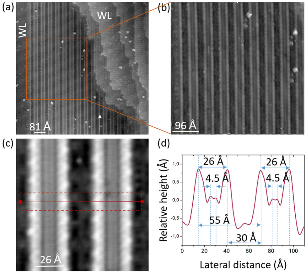 | ||
| Fig. 1 (a) 93.5 × 93.5 nm2 STM topography (−2.4 V, 15 pA) showing a large-scale area of thin ribbons. (b) 46.8 × 46.8 nm2 STM topography (−2.4 V, 16 pA) of a zoomed-in area indicated by the orange square in (a). (c) 110 × 110 Å2 STM topography (−2.4 V, 16 pA) of two consecutive thin ribbons. The red dotted rectangle indicates the area on which lateral line profiles (red line) have been measured and averaged. (d) Variation of the relative height acquired across two thin ribbons as shown in (d) as a function of the lateral distance. | ||
From these variations in tip height, the ensuing measured profile across two ribbons (red line in Fig. 1(c)) is depicted in Fig. 1(d). The sizes of each ribbon are very similar, having a width of ∼26 Å from two maxima. The inner structure of each thin ribbon reveals two central thin stripes separated by 4.5 Å while the period between ribbons is ∼55 Å. Additionally, one can notice that each thin ribbon is periodically spaced out by 30 Å. As a comparison, a previous work reports that large CaF2 ribbons of stripes (i.e. LRS) grown at a lower temperature (710 °C) are made of ribbons of stripes having a single periodicity of ∼11.7 Å.7
The electronic properties of the periodic ribbons can be described via the inelastic electron tunnel spectroscopy (IETS) technique at specific points on the structure. The results of these measurements are presented in Fig. 2(a) where each plotted curve represents the average of 5 measurements at various positions along the designated areas (see Fig. S2 in the ESI† for further details). The inset in Fig. 2(a) shows the four areas where the spectroscopic data are acquired, that is to say, in between two thin ribbons (red curve), at each edge of the thin ribbon (green and blue curves) and in the middle of the ribbon (black curve). There are two main pieces of information in the dI/dV spectrum in Fig. 2(a) about the density of state (DOS) peak distributions in these thin ribbon structures. The first one is that DOS band energies lying between −3.0 V and −2.4 V have similar shapes and intensities. They correspond to a mix of DOSs arising from the silicon subsurface and the observed layer.18 The second DOS distribution is composed of several types of DOS peaks of various linewidths having their maximum voltage in the range 2.4–1.5 V below the surface Fermi level energy. Looking in more detail at the second group of DOS peaks, one can observe that the dI/dV curves are composed of two maximum energies ∼−1.9 eV and ∼−1.6 eV at the edges of the thin ribbon. However, only one DOS peak maximum at ∼1.95 eV below Ef is observed when the spectrum is acquired in between the thin ribbon (red curve) or inside of it (black curve). The very surprising difference in these two spectra resides in their spectral linewidth energies. Indeed, when the dI/dV is acquired beside the periodic thin ribbons, the full width half maximum is 490 meV while equal to 210 meV inside the thin ribbon, which may reveal electronic confinement of the localized density of states at this energy. Note that if one compares these results with the dI/dV signal acquired on an LRS (gray curve in Fig. 2(a), structure reported in ref. 8), our observations indicate that the thin ribbons exhibit a specific electronic structure that is clearly arising from their relatively small size and periodicity. These data can be compared with the dI/dV curves measured on the bare Si(100) surface (dark red curve in Fig. 2(a)). As explained in our previous work,7–9,18 the main role of the CaF2 wetting layer is to passivate the unoccupied surface states of the bare Si(100) surface. This is why one can see that almost all the π* and σ* states disappear in the dI/dV spectrum of the thin ribbons. In the same trend, the π orbitals of the bare Si(100) are restructured due to the partial etching of the surface conducting the dI/dV peak at −1.2 eV to vanish from the bare Si(100) surface. There is, hence, a clear difference between the dI/dV curve arising from the bare Si(100) surface and the ones at the edges of the thin ribbon as the Si σ state DOS peaks are located at different energies. The origin of the dI/dV peaks observed at −1.9 V and −1.6 V at the edges of the thin ribbon can be explained by calculating the projected density of state (PDOS) on one of the additional CaF2 molecules garnishing the edges of the thin ribbons. These calculations are shown in Fig. S3 (ESI†) which indicate two main DOS peaks at 2.2 eV and 1.3 eV below the Fermi energy level that can be reasonably compared to our experimental data.
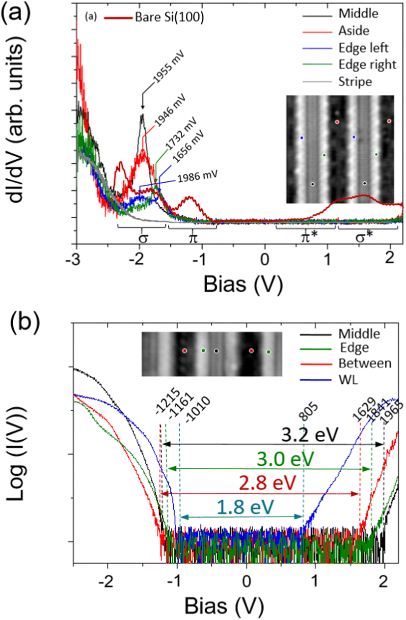 | ||
| Fig. 2 Variation of the dI/dV signal as a function of the bias voltage applied on the sample surface at several locations on (blue, black, green dots) or beside (red dots) the thin ribbons’ structure. (b) Logarithmic scale variation of the tunnel current as a function of the bias voltage for the four indicated positions as shown in the inset in (b). The blue curve is the I(V) signal acquired on the WL area located far beside the thin ribbons as shown in the left part in Fig. 1(a). The values indicated at each edge of the curves are in mV. | ||
To further investigate the electronic properties of the observed periodic thin ribbons, it is necessary to estimate the insulating properties of such structures. Fig. 2(b) exhibits the tunnel current variation when acquired at various positions (see the inset in Fig. 2(b)). On the WL (i.e. beside the periodic thin ribbons Fig. 1(a)), the surface gap energy is relatively small (∼1.8 eV). This value can be considered as a landmark for comparison.8 When the dI/dV curve is acquired in between the thin ribbons, the surface energy gap increases to ∼2.8 eV (red curve in Fig. 2(b)). However, if the dI/dV signal is measured in the central part of the thin ribbon (black curve in Fig. 2(b)) or at its edges (green curve in Fig. 2(b)), the estimated surface gap energy is clearly larger than the previous measurements and worth 3.0 eV and 3.2 eV, respectively.
A similar value of the surface energy gap is measured on LRS (∼3.2 eV)7 indicating that some parts of their structure may be similar. It is also interesting to notice that the energies of the valence band edges in Fig. 2(b) are very similar for each measured position apart from the one at the wetting layer when located far from the periodic thin ribbons (see the WL in Fig. 1(a)). Considering the SK process responsible for the growth of these structures, one can expect that the surface area located in between the thin periodic ribbons would be alike the one of the WL. However, the comparison of the conduction band edge of the red and black curves in Fig. 2(b) indicates that the insulating property of the surface area located in between the thin periodic ribbons is significantly increased compared to the one of the WLs. This indicates that the electronic properties of the area located in between the thin ribbons may arise from a modified WL structure.
To verify the spatial localisation of a DOS enhancement in the center of the thin ribbons, we have measured the distribution of the DOS on a surface area where several thin ribbons are formed (Fig. 3(a)). Simultaneously, the dI/dV signal at the resonance energy as observed in Fig. 2(a) (i.e. −1.95 eV) is acquired for each measured point of the DOS image. The resulting dI/dV map is shown in Fig. 3(b). To help the comparison between Fig. 3(a) and (b), red dotted lines are located on the central axis of the thin ribbons while green dotted lines indicate the common position situated in between the thin ribbons for the two panels.
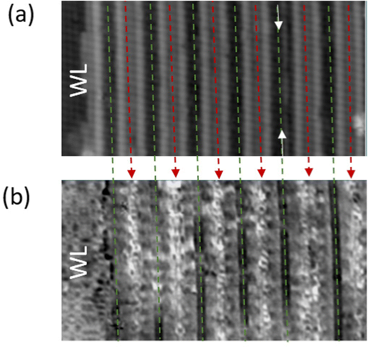 | ||
| Fig. 3 (a) 357 × 176 Å2 STM topography (−2.3 V, 16 pA) of six parallel thin ribbons with a small WL on the left. (b) dI/dV map of the same area as shown in (a) at the bias −1.95 V (see methods for details). The green or red dotted lines are landmarks to locate the positions of the thin ribbons. | ||
It can be noticed that, on the right part of the chosen area, one thin ribbon of stripes is slightly shifted (see the two white arrows) revealing that the periodicity between the thin ribbons can sometimes change on a given terrace. The first surprising observation in Fig. 3(b) is the presence of brighter lines of the dI/dV signal delocalized along the central positions of the periodically spaced thin ribbons. However, while the dI/dV measurements acquired in between the thin ribbons reveal a DOS peak centered at the same resonant energy (Fig. 2), the dI/dV mapping shown in Fig. 3(b) mainly exhibits dark bands (i.e. along the green dotted lines, coherently to what is observed in Fig. 3(a)). Therefore, the enhancement of the DOS signal at the resonant energy 1.95 eV below the Fermi level is only observed at the central part of the thin ribbons (i.e. when the linewidth of the dI/dV peak is worth 210 meV). Yet, one can also notice that, despite the slight shift in the ribbons’ periodicity mentioned previously (see white arrows in Fig. 3(a)), the observed enhancement can still be detected on the ensuing shifted thin ribbons. However, on the left side of the dI/dV mapping area where the randomly arranged WL is covering the silicon surface, the dI/dV mapping exhibits no enhancement. These STM measurements confirm that the spatial distribution of DOS at this resonant energy is confined and delocalized along the central part of the thin ribbons. At this stage of our study, this resonant process seems to arise from the relatively small width of the observed ribbons’ structure.
To bring an additional understanding of the observed periodic thin ribbon structure, we have built a theoretical model of a single thin ribbon unit cell and performed numerical simulations (i.e. annealing and relaxation) by using density functional theory (DFT). Fig. 4(a) recalls a portion of panel c in Fig. 1 in which one can observe various periodical or semi-periodical aspects in the thin ribbon structure (light brown and blue arrows). One of them (light brown arrows) indicates the alternative positions of bright spots located at the external edges of the thin ribbons, having a measured lateral period of ∼14.9 Å. The dark blue arrows point out additional structures on the internal side of the thin ribbons (top panel in Fig. 4(a)) having a measured periodicity of ∼7.5 Å. It is important to recall that the silicon dimer row periodicity of the bare Si(100)-2 × 1 surface is 7.7 Å. A zoomed image of the unit cell of this structure is presented in the lower panel of Fig. 4(a) to be compared with the model structure of a thin ribbon unit cell shown in Fig. 4(b). This structure is composed of the bare Si(100)-2 × 1 surface (blue atoms) on which several WL unit cells having various orientations (see red dotted rectangles and their respective arrows) have grown. The LRS structure, as detailed in a previous work,7 is formed by a superposition of WL unit cells, all oriented in the same direction, in between which are inserted additional CaF2 molecules (see red dotted circles in Fig. 4(b)). The obtained structure forms stripes that expand perpendicularly to the Si dimer row as indicated by the green dotted rectangles. Here, the structure of the thin ribbon is formed via a specific orientation of these stripes as exposed in Fig. 4(b). In particular, one can see that the central part of the thin ribbon is based on two head-to-tail unit cells. Each of them is followed by an additional unit cell having the same direction that forms the edges of the thin ribbon. Hence, the ensuing CaF2 stripes of the thin ribbon follow the same orientation. One of the additional striking aspects of the thin ribbons (Fig. 4(b)) arises from the bright protrusions observed at their edges, which alternate from the left to the right edges of the thin ribbon. We found that these features originate from the presence of additional CaF2 molecules at the edges of the presented structure (see the light brown arrows reported in Fig. 4(b)).
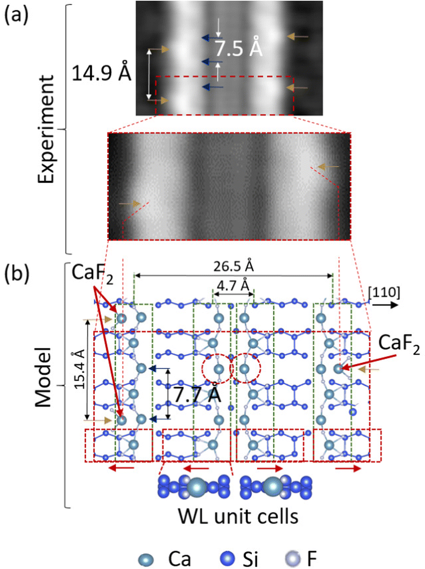 | ||
| Fig. 4 (a) 56.5 × 34 Å2 STM topography (−2.4 V, 16 pA) centered on a small part of a thin ribbon. Blue and light brown arrows indicate the location of the internal or external structure of the ribbon, respectively. The red dotted rectangle shows the zoomed portion of the image presented below. (b) Ball and stick representation of the model structure reproducing the thin ribbon shown in the lower panel of (a). A detailed WL unit-cell is recalled below the figure and its size is reported on the slab via the red dotted rectangles. The red horizontal arrows designate the relative orientation of the WL unit-cell. The green dotted rectangle indicates the stripe structure. Two superimposed red broken lines follow the relative positions of the CaF2 molecules located at the edges of the thin ribbon. The cyan, blue and gray balls are Ca, Si and F atoms, respectively. | ||
To the best of our knowledge, the formation of these periodically spaced superstructures on the Si(100) has never been reported yet. To bring more information on the process responsible for their formation, we have formed a second slab made of two parallel thin ribbons whose structure recalls the unit cell of a single thin ribbon as described in Fig. 4(b). The side and top views of this second structure are presented in Fig. 5(a) and (c) and are related to the experimental data in Fig. 5(b). Having a careful look at Fig. 5(b) reveals more details about the surface area located in between the thin ribbons. Indeed, one can observe that this surface region is not built similarly to the WL8,9 (see for comparison on the left side in Fig. 1(a)). In particular, the STM topography of the surface area that separates the two thin ribbons exhibits a central continuous gray line with scattered dark spots.
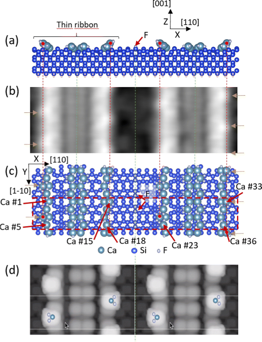 | ||
| Fig. 5 (a) Ball-and-stick representation (side view) of a structure composed of ten silicon layers and two thin ribbons. (b) 102 × 33 Å2 STM topography (−2.45 V, 15 pA) of two consecutive thin ribbons. (c) Balls and sticks representation (top view) of the same slab as in (a). (d) Calculated local density of states images of the slab presented in (a) and (b) at an energy of 2.5 eV below the Fermi level. The cyan, blue and light grey balls are Ca, Si and F atoms, respectively, in the panel (a) and (b). The light brown arrows indicate the relative position of the side additional CaF2 molecules relative to the bright protrusions observed on STM topographies. | ||
At this stage of our understanding, we found that this ensuing surface area is mainly composed of a band of three incomplete WL unit cells placed in a symmetrical way so that fluorine atoms passivate a silicon dimer line at an equal distance of the two consecutive thin ribbons (Fig. 5(a) and (b)). Actually, by comparing Fig. 5(a) and (c) with Fig. 5(b), it can be observed that this second structure allows reproducing the dark grey line centered in between the two thin ribbons observed in Fig. 5(b) (follow the dotted green line) as well as the scattered dark spots appearing at each side of this line (Fig. 5(d)). Yet, one cannot completely exclude that some few missing silicon dimers arising from the initial stage of the WL layer formation may be formed in this area.
The proposed secondary structure of the double thin ribbon model as shown in Fig. 5(a) and (c) accurately describes our experimental finding and, in particular, the alternated white spots observed at their edges. Indeed, the calculated local density of states (LDOS) of this structure shown in Fig. 5(d) for an integrated energy window of 2.5 eV below the Fermi energy can mimic the experimental measurement reported in Fig. 5(b) with a relatively good precision. It is important to notice that for the model of the two thin ribbons presented in Fig. 5, we have chosen to reproduce one of the main trends of our results, i.e. when the additional CaF2 molecules are alternatively located at the two side-by-side edges of the thin ribbons. Although it is possible to observe a conformation where the bright features at the edges of the thin ribbons face each other, their modelization would not change drastically our findings.
One major aspect of the formation of the periodically thin semi-insulating ribbons can be found in Fig. 1(a) where they arise at the edge of a silicon step edge. Since the formation of these periodic structures occurs when the substrate temperature is slightly higher than the formation of LRS (see Section 2.1), one can suggest that the formation of the observed thin ribbons is related to both processes: (i) the epitaxy of the CaF2 molecules on the surface and (ii) the Si(100) 2 × 1 surface reconstruction itself. Indeed, at the selected substrate temperature (∼740 °C), the diffusion of silicon adatoms involved in the formation of the Si(100)-2 × 1 reconstruction is still very high, in particular along the [110] direction i.e. along the silicon dimer rows.24 This temperature range involves especially the formation of the silicon step edges.25 Since we have shown that the first stage formation of the wetting layer formation involves the etching of silicon dimers,7–9 the dynamics of the formation of the observed thin ribbons can clearly be influenced by a slight increase in substrate temperature.
From our observations, the previously reported LRS structure is observed when the silicon surface is heated at a slightly lower temperature (710 °C) compared to the one allowing the formation of the periodically spaced thin ribbons of stripes (740 °C). This relatively small variation of temperature already involves observable differences in the epitaxial surface structure, especially on the WL formation, while the CaF2 coverage is kept constant in both cases. Indeed, as observed in the STM topography in Fig. 1(a), we can see that the silicon surface is fully covered by a WL interface. In contrast, remaining small patches of bare silicon surface are surrounding the LRS.7 This change indicates that the growth switches from a Volmer–Weber (VM) to a Stranski–Krastanov (SK) regime when the temperature slightly increases as mentioned above. Since the misfit between the bulk Si and CaF2 is rather small (i.e. 0.021 Å), the observed growth regime change is thus mainly due to a surface energy alteration.26,27 In our particular case, the surface free energy can significantly vary due to the temperature change, as explained previously because of the increasing diffusion of Si adatoms when the surface temperature reaches 740 °C. The surface energy of the Si(100)-2 × 1 surface can also be affected by the etching process via the CaF2 dissociation that occurs at the first stage of the epitaxy.8 The initial values of the free energies of the two components are γs[Si(100)-2![[thin space (1/6-em)]](https://www.rsc.org/images/entities/char_2009.gif) ×1] = 2.7 meV Å−1 and γ0[CaF2(100)] = 5.7 meV Å−1 where γs and γ0 are the surface energy at the silicon substrate-vacuum interface and the overlayer–vacuum interface, respectively.28 Usually, when γ0 > γs, the VW regime is predominant, which is coherent with our observations when the silicon substrate is kept at a temperature below 710 °C with the growth of LRS structures. However, in the case of a periodic thin ribbon formation, the slight increase in temperature will promote the formation of a full WL, which will completely degrade the initial Si(100)-2 × 1 surface reconstruction, resulting in an additional increase in the silicon surface energy γs to lead to the SK regime.29
×1] = 2.7 meV Å−1 and γ0[CaF2(100)] = 5.7 meV Å−1 where γs and γ0 are the surface energy at the silicon substrate-vacuum interface and the overlayer–vacuum interface, respectively.28 Usually, when γ0 > γs, the VW regime is predominant, which is coherent with our observations when the silicon substrate is kept at a temperature below 710 °C with the growth of LRS structures. However, in the case of a periodic thin ribbon formation, the slight increase in temperature will promote the formation of a full WL, which will completely degrade the initial Si(100)-2 × 1 surface reconstruction, resulting in an additional increase in the silicon surface energy γs to lead to the SK regime.29
Nevertheless, the two previous parameters cannot alone be responsible for the observed periodicity measured between two thin ribbons of stripes (i.e. 55 Å) over areas extending up to 15–20 ribbons. A careful look at the profile in Fig. 1(d) indicates that the thin ribbon width (i.e. ∼26 Å) is about half of the averaged periodicity between two thin ribbons. Since a thin ribbon is, itself, composed of four WL unit cells, this observation indicates that the distance separating two thin ribbons is also related to the size of a WL unit cell. Finally, one can observe that the surface separating two thin ribbons remains darker upon STM topography, indicating that several substitutional Ca atoms are probably missing in these areas as discussed above. Therefore, it can be assumed that the additional CaF2 molecules that aggregate along the edges of the thin ribbons may arise from the surface area formed by the incomplete WL separating two thin ribbons.
The specific orientation of the CaF2 stripes in the thin ribbon structures, as described in Fig. 4(b), may also arise from the influence of the dipole effects on the polar Ca, F and CaF2 components involved in the thin ribbons. To do so, we have plotted a three-dimensional representation of the atomic forces applied on each Ca atom of a slab composed of two consecutive thin ribbons (Fig. 6(a)). The size of the considered slab is depicted by the red dotted rectangle shown in Fig. 5(c). It is composed of 8 rows of 5 Ca atoms (see section 2.2 for details). Each Ca atom is numbered from 1 to 36 in Fig. 5(c). For a better interpretation, the components of each atomic force are projected over the three 2D planes XY, XZ and YZ. Fig. 6(b) presents the projection of the atomic forces on the XY plane and shows the relatively low values of these forces in this plane compared to the z component shown in the other panels in Fig. 6. For guidance, the number of some Ca atoms is recalled. Interestingly, one can observe that the direction of the atomic forces applied to the substitutional Ca atoms of the slab (i.e. Ca No 2, 16, 20 and 34, green circles) is in the opposite direction inside the same thin ribbon (Ca No 2 and 16) and also for the Ca atoms composing two consecutive thin ribbons (Ca No 16 and 20). This is the first indication that the relative orientation of the WL unit cells, as depicted in Fig. 4(b) and 5(c), stabilizes the structure of the thin ribbon. As well, this configuration also stabilizes the interaction between thin ribbons. One can also notice that the Ca atoms forming the CaF2 molecules along the stripes show only weak atomic force components in this plane (see the green dotted circles in Fig. 6(b) for the Ca No 4, 18, 22, 35). Similarly, all the Ca atoms that compose the internal part of the thin ribbon are subject to weak atomic forces.
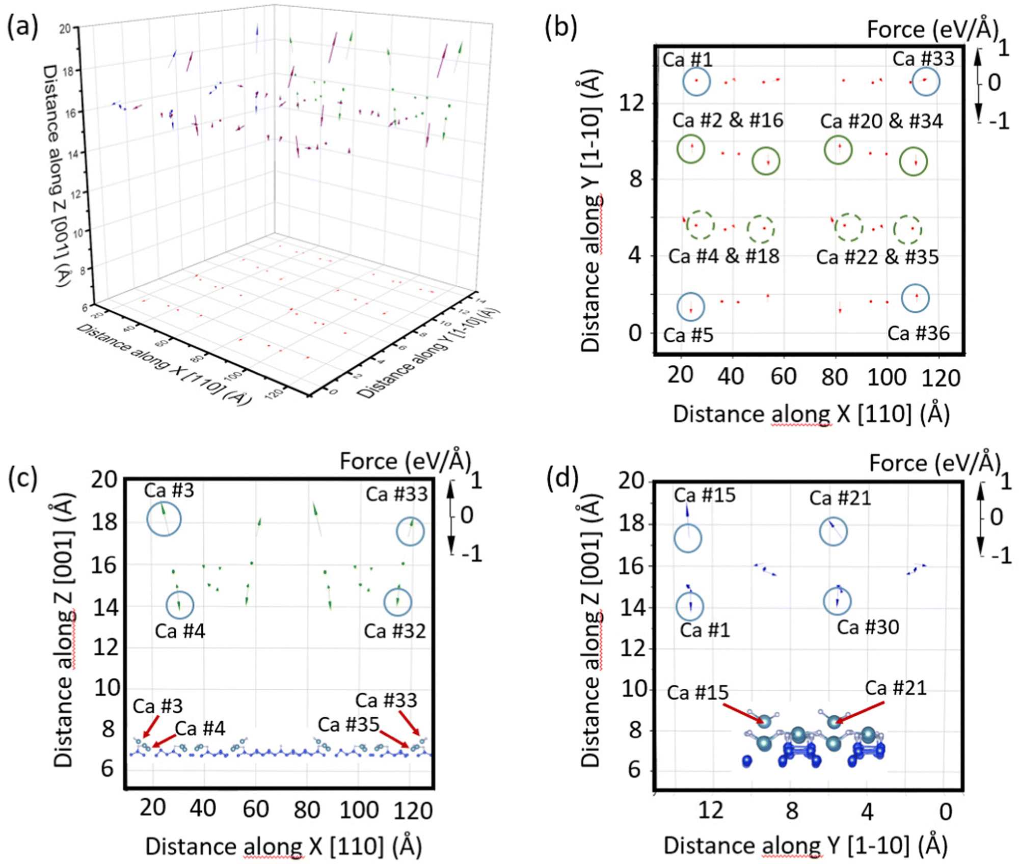 | ||
| Fig. 6 (a) Three-dimensional vectorial representation of the calculated atomic forces (eV Å−1) applied on the Ca atoms of the slab as defined in Fig. 5(c) of a double thin ribbon. (b) to (d) two-dimensional projection of the calculated atomic forces vectors in (a) on the XY, XZ and YZ planes, respectively. The insets in panels (c) and (d) recall a simplified atomic slab of the two thin ribbon model as defined in Fig. 5(c). | ||
Surprisingly, the atomic forces on some of the Ca atoms exhibit components that are mainly perpendicular to the silicon surface (Fig. 6(c) and (d)). These forces appear to be especially acting on the Ca atom numbers 3, 15, 21, and 33 when the z-component is directed upwards. These Ca atoms implicate the CaF2 molecules that agglomerate at the edges of the thin ribbons. Yet, the z-components of the atomic forces directing downwards the surface act on the Ca atom numbers 4, 14, 22 and 32. Here, the involved Ca atoms correspond to some of the CaF2 molecules that intercalate between the WL unit cells, along the stripes. Hence, it appears that the additional free CaF2 molecules that decorate the edges of the thin ribbons stabilize the structure by compensating the forces in the opposite direction. Panel d in Fig. 6 mainly corroborates these trends. In particular, looking at the relative heights of the various Ca atoms shown in the insets in Fig. 6(c) and (d) helps clarify the positions of the discussed Ca atoms.
It would be extremely interesting to further study the influence of various parameters such as the precise substrate temperature, the CaF2 flux or the coverage rate on the growth of the thin insulating ribbons. Moreover, the electronic confinement observed in the periodic thin ribbons could reveal specific physical effects such as anti-corrugating state resonances. These effect could even be enhanced via the use of such structures.18 The study of these effects may surely be the purpose of future investigations, but so far, not in the scope of the present article.
4 Conclusions
In conclusion, we have observed the growth of periodically spaced thin ribbons when the bare Si(100)-2 × 1 surface is exposed to CaF2 molecules in a specific substrate temperature range (∼740 °C). These structures, investigated and analyzed via STM techniques and reproduced by DFT methods, exhibit a periodicity of about half their width over distances that can exceed 80 nm. The observed thin ribbons show semi-insulating properties similar to LSR previously studied (i.e. ∼3.2 eV). One of their particularities is that the thin ribbons exhibit a resonant state at ∼1.95 eV below the surface Fermi energy with a relatively low linewidth of 210 meV. Such a resonant DOS peak could be exploited via the opening of specific planar transport channels in molecular adsorbates by adding contacting pads nearby these structures.15 Considering the ensemble of their properties, the observed periodic semi-insulating thin ribbons may be attractive in various scientific communities having fundamental interest in condensed matter physics, surface chemistry or molecular electronics as well as, for more applied purposes, those dealing with microelectronics including FINFET transistors that are nowadays reaching sizes that are comparable to the width of the observed ribbons. Our finding thus paves the way to a very interesting novel method that will allow the precise localization of not only insulating structures but also any islands that use epitaxy techniques in the VM or SK growth regimes.Author contributions
DR performed the experimental measurements and data analysis and mainly wrote the article. ED performed the DFT simulations on the large atomic slab. DR participated as well in the DFT simulations discussions. All the authors contributed to the writing and proofreading of the manuscript.Conflicts of interest
There are no conflicts of interest to declare.Acknowledgements
All the authors wish to thank the French National Agency for Research (ANR) for their financial support of the CHACRA project under the contract number ANR-18-CE30-0004-01. This work was supported (under the same contract) by the Mesocentre of Université de Franche Comté that granted its access for DFT simulations. DR would also like to thank the Mésocentre LUmière Matière (MésoLUM) at ISMO for granting access to their computational resources.References
- J. Repp, G. Meyer, S. Paavilainen, F. E. Olsson and M. Persson, Imaging bond formation between a gold atom and pentacene on an insulating, Surf. Sci., 2006, 312, 1196–1199 CAS.
- W.-W. Hsu, J. Y. Chen, T.-H. Cheng, S. C. Lu, W.-S. Ho, Y.-Y. Chen, Y.-J. Chien and C. W. Liu, Surface passivation of Cu(In,Ga)Se2 using atomic layer deposited Al2O3, Appl. Phys. Lett., 2012, 100, 023508 CrossRef.
- F. W. Smith and G. Ghidini, Reaction of oxygen with Si(111) and (100): Critical conditions for the growth of SiO2, J. Electrochem. Soc., 1982, 129, 1300 CrossRef CAS.
- L. Pasquali, S. M. Suturin, A. K. Kaveev, V. P. Ulin, N. S. Sokolov, B. P. Doyle and S. Nannarone, Interface chemistry and epitaxial growth modes of SrF2 on Si(001), Phys. Rev. B: Condens. Matter Mater. Phys., 2007, 75, 075403 CrossRef.
- H. Rauscher, T. A. Jung, J.-L. Lin, A. Kirakosian, F. J. Himpsel, U. Rohr and K. Müllen, One-dimensional confinement of organic molecules via selective adsorption on CaF1versus CaF2, Chem. Phys. Lett., 1999, 303, 363–367 CrossRef CAS.
- T. Sumiya, Initial growth stages of CaF on Si(111) investigated by scanning 2 tunneling microscopy, Appl. Surf. Sci., 2000, 156, 85–96 CrossRef CAS.
- M. A. Gribelyuk and G. D. Wilk, Growth and microstructure of Si/CaF2/Si(111) heterostructures, Thin Solid Films, 1999, 339, 51–57 CrossRef CAS.
- E. Duverger, A. G. Boyer, H. Sauriat-Dorizon, P. Sonnet, R. Stephan, M.-C. Hanf and D. Riedel, Two-dimensional functionalized ultrathin semi-insulating CaF2 layer on the Si(100) surface at a low temperature for molecular electronic decoupling, ACS Appl. Mater. Interfaces, 2020, 12, 29661–29670 CAS.
- F. Chiaravalloti, G. Dujardin, D. Riedel, H. P. Pinto and A. S. Foster, Atomic-scale study of the adsorption of calcium fluoride on Si(100) at low-coverage regime, Phys. Rev. B: Condens. Matter Mater. Phys., 2011, 84, 155433 CrossRef.
- F. Chiaravalloti, G. Dujardin and D. Riedel, Atomic scale control of hexaphenyl molecules manipulation along functionalized ultra-thin insulating layer on the Si(100) surface at low temperature (9 K), J. Phys.: Condens. Matter, 2015, 27, 054006 CrossRef CAS PubMed.
- A. Klust, T. Ohta, A. A. Bostwick, E. Rotenberg, Q. Yu, F. S. Ohuchi and M. A. Olmstead, Electronic structure evolution during the growth of ultrathin insulator films on semiconductors: From interface formation to bulklike CaF2/Si(111) films, Phys. Rev. B: Condens. Matter Mater. Phys., 2005, 72, 205336 CrossRef.
- F. Calleja, J. J. Hinarejos, A. A. Vázquez de Parga, S. M. Suturin, N. S. Sokolov and R. Miranda, Epitaxial growth of CaF2(111) on Cu(111) visualized by STM, Surf. Sci., 2005, 582, 14–20 CrossRef CAS.
- L. Pasquali, S. M. Suturin, V. P. Ulin, N. S. Sokolov, G. Selvaggi, A. Giglia, N. Mahne, M. Pedio and S. Nannarone, Calcium fluoride on Si(001): Adsorption mechanisms and epitaxial growth modes, Phys. Rev. B: Condens. Matter Mater. Phys., 2005, 72, 045448 CrossRef.
- A. Z. Alzahrani and D. Usanmaz, Progressive changes in surface structure and electronic properties on Si(001) surface by CaF2 adsorption, J. Appl. Phys., 2011, 109, 123708 CrossRef.
- M. Yengui, E. Duverger, P. Sonnet and D. Riedel, Translational manipulation of magnetic cobalt adatoms on the Si(100)-2 × 1 surface at 9 K, J. Phys. Chem. C, 2019, 123, 26415–26423 CrossRef CAS.
- M. Yengui and D. Riedel, Evidence of low Schottky barrier effects and the role of gap state in the electronic transport through individual CoSi2 silicide nano-islands at low temperature (9 K), J. Chem. C, 2015, 119, 22700 CrossRef CAS.
- M. Yengui, E. Duverger, P. Sonnet and D. Riedel, A Two-dimensional on/off switching device based on anisotropic interactions of atomic quantum dots on Si(100):H., Nat. Commun., 2017, 8, 2211 CrossRef PubMed.
- D. Riedel, M. Lastapis, M. G. Martin and G. Dujardin, Influence of tip-surface interactions and surface defects on Si(100) surface structures by low-temperature (5 K) scanning tunneling microscopy, Phys. Rev. B: Condens. Matter Mater. Phys., 2004, 69, 121301 CrossRef.
- M. Yengui, H. Pinto, J. Leszczynski and D. Riedel, Atomic scale study of corrugating and anticorrugating states on the bare Si(100) surface, J. Phys.: Condens. Matter, 2015, 27, 045001 CrossRef CAS PubMed.
- P. Ordejon, E. Artacho and J. M. Soler, Self-consistent order-N density-functional calculations for very large systems, Phys. Rev. B: Condens. Matter Mater. Phys., 1996, 53, 10441–10444 CrossRef PubMed.
- J. M. Soler, E. Artacho, J. D. Gale, A. García, J. Junquera, P. Ordejón and D. Sánchez-Portal, The SIESTA method for ab initio order-N materials simulation, J. Phys.: Condens. Matter, 2002, 14, 2745–2779 CrossRef CAS.
- J. P. Perdew, K. Burke and M. Ernzerhof, Generalized gradient approximation made simple, Phys. Rev. Lett., 1996, 77, 3865–3868 CrossRef CAS PubMed.
- K. Lee, É. D. Murray, L. Kong, B. Lundqvist and D. C. Langreth, Higher-accuracy van der Waals density functional, Phys. Rev. B: Condens. Matter Mater. Phys., 2010, 82, 081101 CrossRef.
- S. H. Lim, S. Song, T. S. Park, E. Yoon and J. H. Lee, Si adatom diffusion on Si(100) surface in selective epitaxial growth of Si, J. Vac. Sci. Technol., B: Microelectron. Nanometer Struct.--Process., Meas., Phenom., 2003, 21, 2388 CrossRef CAS.
- G. D. Lee, S. Hong, H. W. Kim and E. Yoon, Diffusion of adatom in the selective epitaxial growth of Si(100): A molecular dynamics study, Appl. Phys. Lett., 2006, 88, 231909 CrossRef.
- M. H. Grabow and G. H. Gilmer, Thin film growth modes, wetting and cluster nucleation, Surf. Sci., 1988, 194, 333–346 CrossRef CAS.
- E. Bauer, Epitaxy of metals on metals, Appl. Surf. Sci., 1982, 11/12, 479–494 CrossRef.
- Encyclopedia of materials [Texte imprimé]: science and technology, ed. K. H. Jürgen Buschow, Elsevier, Amsterdam, 2001 Search PubMed.
- S. Somasi, B. Khomami and R. Lovett, Computer simulation of the surface free energy of the Si(100) surface and the line free energies associated with steps on this surface, J. Phys. Chem. B, 2004, 108, 19721–19728 CrossRef CAS.
Footnote |
| † Electronic supplementary information (ESI) available. See DOI: https://doi.org/10.1039/d2ma00751g |
| This journal is © The Royal Society of Chemistry 2022 |