
 Open Access Article
 This Open Access Article is licensed under a Creative Commons Attribution-Non Commercial 3.0 Unported Licence
Lead-free AgBiI4 perovskite artificial synapses for a tactile sensory neuron system with information preprocessing function†
Haibo
Ye
a,
Zhiyong
Liu
*a,
Hangdi
Han
a,
Tielin
Shi
a and
Guanglan
Liao
 ab
ab
aState Key Laboratory of Digital Manufacturing Equipment and Technology, Huazhong University of Science and Technology, Wuhan, 430074, China. E-mail: zhiyong_liu@hust.edu.cn
bShenzhen Huazhong University of Science and Technology Research Institute, Shenzhen, 518057, China
First published on 29th July 2022
Abstract
Organometal halide perovskites (OHPs) exhibit great potential in memristors and artificial synaptic devices. However, the toxicity of lead and instability set barriers for further applications in neuromorphic computing. Herein, we demonstrate an artificial synapse based on inorganic lead-free AgBiI4 perovskites, which exhibits typical analog resistive switching (RS) characteristics and synaptic behaviors. Several functions of biological synapses are realized including long-term potentiation (LTP), long-term depression (LTD), paired-pulse facilitation (PPF) and spike-timing-dependent plasticity (STDP). Furthermore, by integrating a tactile sensor array with a AgBiI4 synaptic device, an artificial sensory neuron system is demonstrated. Under pressure stimulations with various intensities, an electrical pre-synaptic signal is transferred to artificial synapses for further information preprocessing, realizing the capability of contrast enhancement and noise reduction. After information preprocessing with an artificial sensory neuron system, the recognition accuracy reaches up to almost 100% with only 500 training epochs by using the MNIST handwritten data set. The presented work provides a new candidate for the next generation of neuromorphic computation based on lead free perovskites.
1. Introduction
With the increasing requirements of fast processing of large amounts of data and information in sensing systems, traditional von Neumann architecture, where the data transfer speed between the central processing unit and the memory is limited, is facing severe constraints such as Moore's law limit, storage walls, and high energy consumption.1,2 The human brain composed of a high-density synapse network is capable of highly parallel information processing.3,4 Thus, building a computer architecture similar to the human brain nervous system is considered to be promising for overcoming the limitations of von Neumann computing systems. Neuromorphic computing systems composed of electronic neurons and synapses achieve a high degree of parallelism with the physically united memory and processing units. Among them, the artificial synapse is the fundamental unit in the neuromorphic computing system, which is able to emulate essential synaptic functions in a single electronic device, which consumes only femtojoule-level amounts of energy.4–7 In a sensing system, integrating sensors with artificial synapses with short-term plasticity and long-term plasticity instead of conventional complementary metal-oxide semiconductor (CMOS) circuits not only reduces the amount of hardware and power consumption but also achieves first-stage data processing function and boosts the data transfer speed.8–10 The next-generation synaptic devices are concentrated on metal oxide semiconductors,11 organic semiconductors,12 and 2D materials,13 where tradeoffs are always required between the advantages and associated shortcomings.In the last few years, organometal halide perovskites (OHPs) have attracted large amounts of attention for their remarkable performance in solar cells, which is attributed to their outstanding material properties (strong optical absorption, tunable band gap, ambipolar charge transport, and long electron–hole diffusion length).14–24 In 2020, Zeng et al. reported a blade-coated perovskite solar cell with a self-assembled monolayer, achieving a power conversion efficiency of 14.13%.25 In addition to the application in solar cells, OHPs also have great potential in an artificial synaptic device. In 2015, Xu et al. reported the first artificial synapse based CH3NH3PbBr3 perovskite, emulating important synaptic characteristics in a single electronic device successfully.4 Since then, a variety of OHP artificial synapses have been reported.10,26–30 In 2020, Pi et al. reported an optically stimulated synaptic device based on the hybrid structure of silicon nanomembranes and perovskites, which has great potential in the field of multi-functional and low energy consumption synaptic devices.31–33 However, the toxicity of lead and the intrinsic instability caused by the organic group in OHPs limit the further practical and commercial application of OHP-based artificial synapses in neuromorphic computing. Consequently, it is absolutely necessary to further explore the non- or low-toxicity and stable perovskite material to promote the commercial applications of perovskite artificial synapses.31,34–36 To solve this problem, large amounts of efforts such as Sn2+, Ge2+, Bi3+ and Sb3+.37–40 have been taken. However, the intrinsic instability of Sn or Ge caused by the easy oxidation of Sn2+ to Sn4+ or Ge2+ to Ge4+ when being exposed to ambient air still has not been solved well.41,42 Low-toxicity and stable Bi3+ and Sb3+ represent another candidate to replace Pb, offering a similar ionic radius and identical electronic structure to Pb2+. Recently, a perovskite compound A3B2X9 (B = Bi, Sb) is studied for lead-substitution. Hu et al. have reported a flexible memristor based on Cs3Bi2I9 perovskites.43 Paramanik et al. studied the resistive switching (RS) and artificial synaptic behaviors in layered Cs3Sb2I9 lead-free perovskites.44 Nevertheless, the structure of the A3B2X9 perovskite exhibits low-dimensional (0 and 2D) and demonstrates unfavorable optoelectronic properties.45 The Ag–Bi–I ternary family is another promising candidate for lead-free perovskite materials. Lu et al. achieved a power conversion efficiency of 2.1% based on the AgBiI4 perovskite.46 Pecunia et al. fabricated the near-infrared (NIR)-blind visible light photodetection based on Ag2BiI5.47 In our previous work, we have reported a lead-free AgBiI4 flexible memristor with an ultralow operating voltage of 0.16 V.48 However, to the best of our knowledge, there is no relevant report on the application of the Ag–Bi–I ternary family in the field of artificial synapses.
In this work, we demonstrate an artificial synapse based on the lead-free inorganic AgBiI4 perovskite with a structure of Ag/polymethylmethacrylate (PMMA)/AgBiI4/FTO. The synaptic devices exhibit typical bipolar analog RS characteristics and various functions of biological synapses are realized such as long-term potentiation (LTP), long-term depression (LTD), paired-pulse facilitation (PPF) and spike-timing-dependent plasticity (STDP). After integrating the AgBiI4 synaptic device with a tactile sensor, an artificial sensory neuron system is demonstrated which can respond to the pressure stimulations with various intensities and realize the capability of contrast enhancement and noise reduction. For Modified National Institute of Standards and Technology (MNIST) data set image recognition, the simulation results show that the device achieves an accuracy of almost 100% with the artificial sensory neuron system after only 500 training epochs, higher than the accuracy of 98% without information preprocessing.
2. Results and discussion
The artificial synaptic devices are fabricated based on the lead-free AgBiI4 perovskite with a structure of Ag/PMMA/AgBiI4/FTO (Fig. 1a). The insertion of the PMMA layer is to protect the AgBiI4 perovskite film from the diffusion of the metal electrode layer. Besides, the direct contact of Ag and perovskite would result in the formation of a layer of AgIx at the interface, affecting the RS characteristics of the synapse devices.49 The AgBiI4 perovskite film is synthesized by a hot casting method.50 In brief, the precursor solution is spin-coated on the preheated FTO substrate, followed by the anti-solvent treatment. The temperature of the substrate is a key parameter to obtain high quality and pinhole-free films. The insufficient temperature would result in poor film coverage. Besides, the thickness of the film also highly depends on the preheated temperature. It is reported that substrate preheat treatment will significantly increase the thickness of the CsPbIBr2 perovskite.51 Similarly, a higher preheating temperature will promote the evaporation of the solvent and facilitate the formation of high quality and thick AgBiI4 layer. Fig. 1b depicts the X-ray diffraction (XRD) patterns of the AgBiI4 film. Strong diffraction peaks at 12.75°, 23.94°, 25.76°, 29.29° and 41.43° can be assigned to the (111), (311), (222), (400) and (440) planes of the AgBiI4 cubic-phase structure.52 Peaks marked as * imply the existence of Ag2BiI5. The top-view scanning electron microscopy (SEM) image of the AgBiI4 film is shown in Fig. 1c. The as-prepared film is dense and non-porous with an average grain size of approximately 150 nm. The energy-dispersive X-ray spectra (EDS) in Fig. S1 (ESI†) clearly indicate that the Ag, Bi and I elements are uniformly distributed on the surface of the film. The cross-sectional scanning electron microscope (SEM) image of the whole device depicted in Fig. 1d demonstrates a well-defined layer-by-layer structure with sharp interfaces. The PMMA layer introduced between the perovskite layer and the Ag electrode is too thin to observe. The thickness of the AgBiI4 perovskite layer is about 1 μm. The atomic force microscopy (AFM) characterization is further performed to characterize the surface morphology (Fig. S2, ESI†). The root mean square (RMS) roughness is calculated to be 36.2 nm. The X-ray photoelectron spectroscopy (XPS) test is also conducted to study the elemental compositions in the AgBiI4 films. The XPS spectrum shows the presence of Ag, Bi, and I (Fig. S3, ESI†). As shown in Table S1 (ESI†), the atomic percentages of Ag, Bi, and I are 9.18, 9.44, and 42.38%, indicating that the atomic ratio of Ag, Bi, and I on perovskite films is around 1![[thin space (1/6-em)]](https://www.rsc.org/images/entities/char_2009.gif) :1:4.
:1:4.
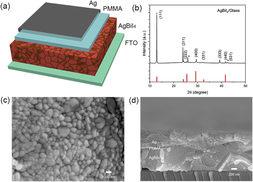 | ||
| Fig. 1 (a) Schematic illustration of the AgBiI4 artificial synapse structure. (b) The experimental and reference (red lines) XRD patterns of the as-prepared AgBiI4 perovskite layer. (c) The top-view SEM image of the AgBiI4 perovskite layer. (d) The cross-sectional SEM image of the whole device. | ||
The RS characteristics are investigated by analyzing the current–voltage (I–V) curves of the Ag/PMMA/AgBiI4/FTO devices. The I–V curve is carried out in the DC sweeping mode. An external bias sweeping in a routine of 0 → 3.0 → 0 → −3.0 → 0 V is applied to the Ag electrode with the grounded FTO electrode. A current compliance of 0.01 A is set up to prevent the permanent breakdown of the device. As shown in Fig. 2a, the device is set at a high resistance state (HRS) before the voltage sweep. When a positive voltage sweep (0 → 3.0 V → 0 V) is applied on the Ag electrode, the device is switched to the LRS and remains in the LRS during the reverse voltage sweep. The resistance state of the device is reversed from the HRS to the LRS when a negative voltage sweep (0 → −3.0 V → 0 V) is applied. To investigate the role of the PMMA layer in the RS behavior of synaptic devices, the I–V characteristic of the PMMA layer with a structure of ITO/PMMA/Ag is performed. The PMMA layer shows no RS behavior under cyclic scanning from 1 V to −1 V and has little effect on the RS behavior of the synaptic devices (Fig. S4a, ESI†). The ultrathin PMMA layer acts as a protective layer not only avoiding the reaction of the perovskite film with the top electrode but also protecting the perovskite film from moisture and oxygen under ambient conditions. The device without the PMMA layer exhibits a similar RS behavior and a higher ON/OFF ratio (Fig. S4b, ESI†). This can be attributed to the formation of AgIx between the Ag electrode and the AgBiI4 layer. The double logarithmic scale of the I–V curve in the positive sweep is shown in Fig. S5 (ESI†). In the HRS, the slope fitted by the curve is 1.08 and 2.39, displaying an ohmic region and a Child's law region, respectively, where the space charge limited current (SCLC) conduction occurs. In the LRS, a slope of 1.19 corresponds to an ohmic region indicating the formation of conductive filaments in this transition process. A previous study has demonstrated that the Ag filaments play a leading role in the RS process of AgBiI4 memristor.48 However, the thickness of the AgBiI4 layer reaches up to almost 1 μm in this study and the RS characteristic is totally different from the previous study. It is worth noting that the thickness of the medium layer also plays a significant role in the mechanism of RS, where two types of conductive filaments can coexist in a single memory cell.53 Here, we suppose that when the thickness of the medium layer becomes larger, the I vacancy defects (VI) are responsible for the RS mechanism instead of Ag conductive filaments which usually require a larger electric field.19 The migration of VI in the AgBiI4 film causes the formation/rupture of the conductive filaments and the schematic diagram for the RS mechanism is illustrated in Fig. S6 (ESI†). In the initial state, the VI is evenly distributed in the perovskite film. During the set process, when a positive bias is applied on the Ag top electrode, the VI tends to migrate to the ITO electrode. VI filaments may be formed and become connected from the bottom electrode to the top electrode. During the reset process, the VI tends to migrate to the Ag electrode, resulting in the fracture of VI filaments.
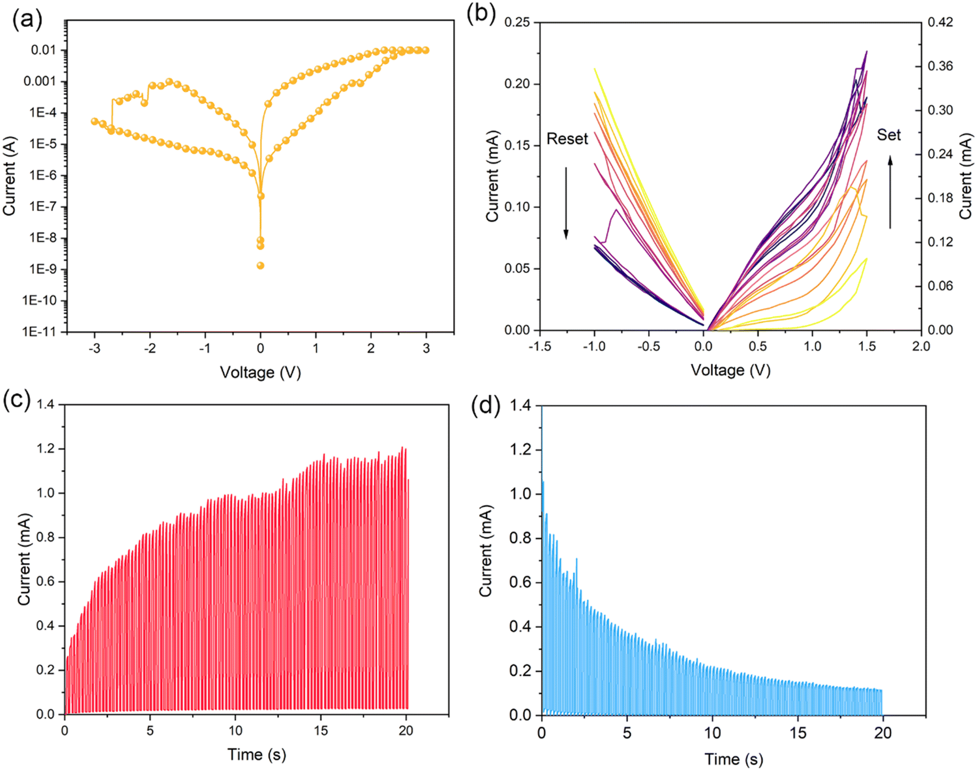 | ||
| Fig. 2 (a) Typical current–voltage (I–V) curve of the AgBiI4 artificial synapse under positive and negative sweeps. (b) I–V curves under 10 positive and 10 negative voltage sweeps (0 → 1.5 → 0 → −1.0 → 0 V). (c) The EPSC plasticity with positive pulses (1.5 V, 0.1 s). (d) The EPSC plasticity with negative pulses (−1.5 V, 0.1 s). | ||
During the Set process, the resistance of the device decreases continuously from the HRS to the LRS, which is similar to the transmission characteristics of the biological synapse. To assess the consecutively tunable resistance states accurately, smaller continuous voltage sweeps (0 → 1.5 → 0 → −1.5 → 0 V) are applied on the device to carefully control the change of resistances. As shown in Fig. 2b, when 10 consecutive sweeps of positive voltage are applied to the device, the current increases after each sweep. Subsequently, after applying 10 consecutive sweeps of negative voltage, the current gradually decreased with the increase of voltage sweep number. Different from devices that show sudden conductance variation in memristors with binary states, the conductance of the AgBiI4 device varies gradually under both positive and negative sweeps, implying that the AgBiI4 device emulates a successively variable synaptic weight. To further evaluate the modulable synaptic plasticity, 100 repeated positive voltage pulses (1.5 V, 0.1 s) are applied to the device for potentiation, followed by 100 negative voltage pulses for depression. As shown in Fig. 2c and d, the excitatory postsynaptic current (EPSC) increases with the increase of the positive pulses and exhibits the opposite change under negative pulses. The modulable synaptic plasticity behaviors resemble the synaptic LTP and LTD processes of the biological synapse. To investigate the stability of the synaptic devices based on the AgBiI4 perovskite, the unsealed device is put in an ambient environment for 100 days. Fig. S7 (ESI†) shows the LTP and LTD characteristics of the device before and after storage, which confirms the good stability of our AgBiI4-based devices.
The biologic synaptic plasticity is a change in synaptic weight in response to stimuli, which serves as a bridge between two neurons to transmit information and is the basis of learning and memory. In the AgBiI4 perovskite devices, the Ag electrode and the FTO electrode emulate presynaptic and postsynaptic neurons, respectively, realizing the learning and memory functions of the human brain including STP and LTP by controlling the input voltage. Fig. 3a depicts the spike-duration-dependent plasticity (SDDP) of the AgBiI4 perovskite synaptic devices. Electrical stimuli with different pulse widths ranging from 0.1 to 1.1 s are applied to the synaptic device. The EPSC peaks increase gradually with the increase of pulse width, implying that a larger synaptic weight will be achieved under a longer-duration pulse. The effect of the voltage amplitude on the synaptic plasticity is also studied (Fig. 3b). With a fixed pulse width, the EPSC increases with the increase of pulse amplitude, indicating that the AgBiI4 perovskite synaptic device has the function of spike-voltage dependent plasticity (SVDP). Besides, the spike-number dependent plasticity (SNDP) can also be mimicked with different numbers of voltage pulses. As shown in Fig. 3c, the increase in the pulse numbers results in a larger EPSC response.
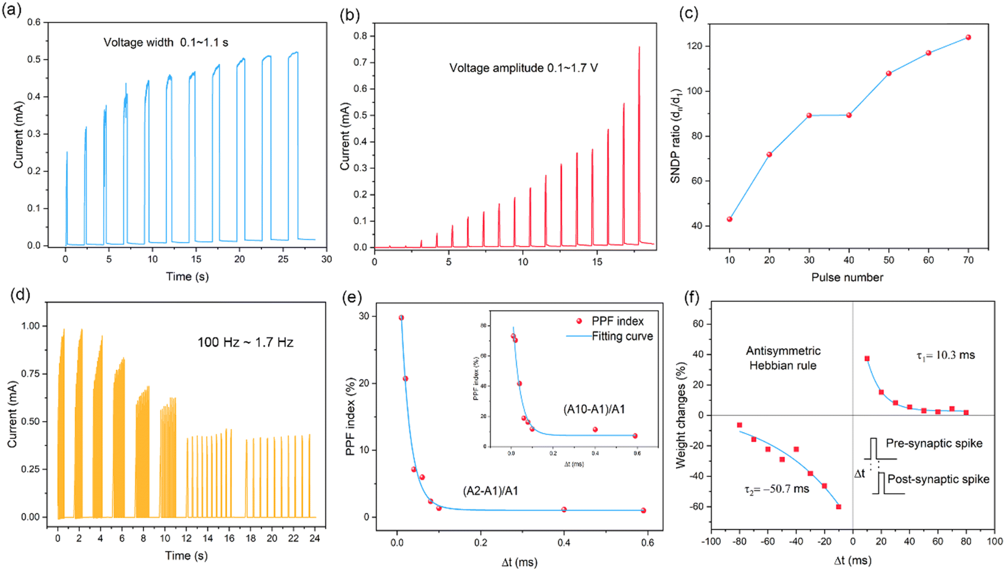 | ||
| Fig. 3 (a) The EPSC with the pulse duration from 0.1 to 1.1 s (1.0 V). (b) The EPSC with the pulse voltage amplitude from 0.1 to 1.7 V (0.1 s). (c) SNDP ratio versus pulse number stimulated by different numbers of voltage pulses. (d) The EPSC with a pulse frequency from 1.7 to 100 Hz. (e) PPF index versus time interval between two successive pulses (1.5 V, 0.05 s). Inset: PPF index versus time interval between the 1st and the 10th pulse (1.5 V, 0.05 s). (f) STDP-like behaviors in the AgBiI4 based artificial synapses. The reading voltage applied above is 0.1 V. | ||
The spike-frequency dependent plasticity (SFDP) is an important characteristic of synaptic devices, which is related to learning, associative memory, and forgetting. This phenomenon in biological synapses is that the response to the stimuli which comes after the first stimuli will be enhanced within a short interval. Similarly, the change of the synaptic weight in the perovskite synapse also depends on the paired-pulse interval. To evaluate the PPF for STP of the synaptic devices, ten synaptic spikes with various frequencies (1.7, 2.5, 10, 12.5, 16.7, 25, 50 and 100 Hz) are applied to the devices. As shown in Fig. 3d, with the decrease of the spike frequency, the EPSC exhibits a downward trend, indicating that smaller paired-pulse intervals lead to much higher EPSC excited by the second pulse. The PPF index is calculated from the following equation:
| PPF index = (A2 − A1)/A1 |
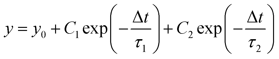
where Δt is the paired-pulse interval, y0 is the resting facilitation magnitude, C1 and C2 are facilitation constants, and τ1 = 22 ms and τ2 = 52 ms are the characteristic relaxation time.
Another essential function of the synapse is STDP, also known as the Hebbian learning rule, which can evaluate temporal correlations between the pre-synaptic and post-synaptic spikes. Four forms of STDP behaviors have been discovered in the biological synapse, which have different functions regarding information processing and storage. Here the asymmetric Hebbian learning rule is realized, where a post-synaptic spike arriving after the pre-synaptic spike (Δt > 0, Δt = tpost − tpre) will lead to LTP of the synapse and the post-synaptic spike arriving before the pre-synaptic spike (Δt < 0) leads to LTD. The change of weight (ΔW) in asymmetric Hebbian can be fitted by the following equation:55
In the human tactile sensing system, the action spikes generated by the mechanoreceptors under tactile input transmit along the afferent axons to synapses. Then, the synapses preprocess the information and relay it to neurons for further processing, as depicted in Fig. 4a. The mechanoreceptors in the skin are able to encode the tactile stimuli as an action potential and the synapse is a connecting bridge between pre- and post-neurons for brain functions such as learning, forgetting, and memory. To emulate the human tactile sensing system, an artificial sensory neuron system is demonstrated by integrating a tactile sensor array with the AgBiI4 synaptic device. The photographs of the AgBiI4 artificial synaptic device and the tactile sensor are depicted in Fig. S8 (ESI†). The sensor arrays consist of a pressure-sensitive film addressed by a network of orthogonal conductive threads on each side. Each point of overlap between the orthogonal electrodes is sensitive to normal pressure, modulating the resistance through the pressure-sensitive film. The pressure response of a single sensing element is shown in Fig. S9 (ESI†), changing from about 750 Ω (1 N) to 250 Ω (5 N). In the AgBiI4 synaptic devices, the TE and BE serve as the pre-synaptic input and the post-synaptic output respectively, while the change of resistance is regarded as the potentiation or depression of the synaptic weight. Therefore, after the pressure signals being transformed in to the pre-synaptic by the sensor array, the changes in synapse resistance can be obtained by the post-synaptic current. Next, the post-synaptic current can be subsequently input into the artificial neural networks (ANNs) which work as the brain for further recognition. Fig. 4b displays the schematic illustration of the artificial sensory neuron system, the tactile sensor is connected with the synaptic device in series. A source-meter is utilized to applied voltage spikes to the tactile sensor and the synaptic device. Finally, the post-synaptic output currents are relayed to the artificial neural network for further processing.
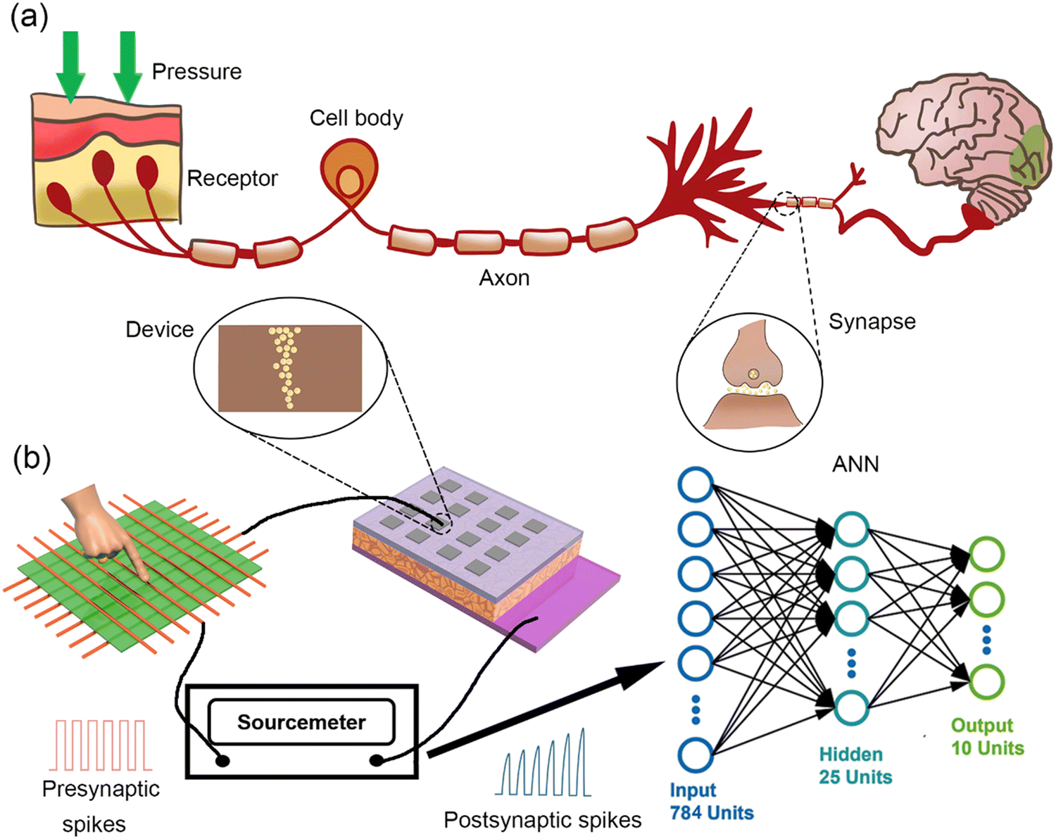 | ||
| Fig. 4 (a) Schematic illustration of the biological tactile sensing system. (b) The artificial sensory neuron system consisting of tactile sensors, perovskite artificial synapses and ANNs. | ||
Unlike conventional sensory systems based on the CMOS technology, the synapses in the artificial sensory neural system can directly preprocess the information transmitted from the tactile sensor with reductions in the amount of hardware and power consumption. The information preprocessing of the artificial sensory neuron system is carried out based on pressure-dependent plasticity. Fig. 5a depicts the output current as the function of pressure applied to the mechanoreceptors, where the input pressure intensity is set to be 1.0 N, 1.6 N, 2.6 N and 5.5 N, and the corresponding voltage on the synaptic device is measured to be 0.7 V, 0.9 V, 1.1 V and 1.4 V. The EPSC increases as the pressure increases from 1.0 N to 5.5 N. Then, 20 repeated voltage spikes are applied to the system to carry out a training process. As shown in Fig. 5b, after repeated training, the difference between the output currents is enlarged according to the different pressures. The increase in the rate of the output current with a higher pressure is higher than that with a lower pressure intensity. The currents with a lower intensity decay faster, whereas the currents with a higher intensity decay slower. In this way, the main feature in one image is highlighted, and the image contrast is enhanced. The relationship between the output current and input pressure is established for the artificial sensory neuron system by fitting the experimental results, where the current and the pressure are normalized from 0 to 1. The data is fitted well with a power function (Fig. 5c):
| y = axb |
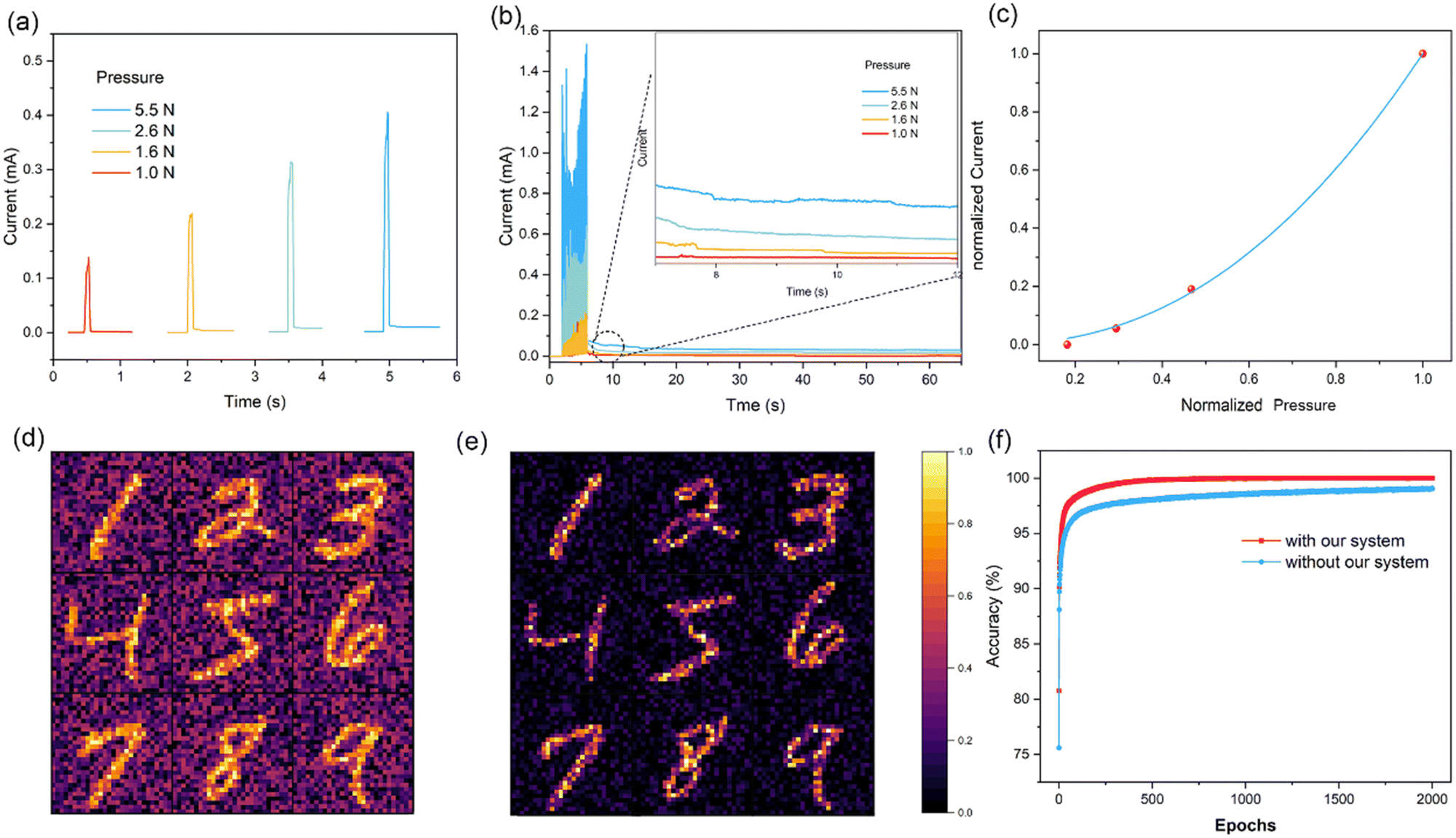 | ||
| Fig. 5 (a) The EPSC with different pressure. (b) The training process carried out with repeated pressure pulses (repeated 20 times) for the artificial sensory neuron system. (c) The normalization of the current–pressure curve based on the output current of the artificial sensory neuron system. (d) The images of figure 1–9 in the MNIST database. (e) The images of figure 1–9 in the MNIST database after being preprocessed by the artificial sensory neuron system (f) Comparisons of the image recognition accuracy for the MNIST patterns with and without the image preprocessing. | ||
3. Conclusion
In summary, an artificial synapse based nontoxic AgBiI4 perovskite is successfully fabricated, which exhibits typical bipolar analog RS characteristics. The basic biological synaptic functions such as LTP, LTD, PPF and STDP are successfully mimicked. Furthermore, an artificial sensory neuron system is demonstrated by integrating the synaptic device with tactile sensors, which are capable of information preprocessing and further realizing the functions of contrast enhancement and noise reduction. The pattern recognition accuracy reaches up to almost 100%, higher than the accuracy of 98% without information preprocessing. Our work opens up new avenues for the realization of neuromorphic computation based on lead-free perovskites.4. Experimental section
4.1 Materials
The FTO substrates with a 14 Ω □−1 resistance (NSG-14) were purchased from Nippon Sheet Glass Co. Ltd., Japan. Anhydrous ethanol, acetone, and dimethyl sulfoxide (DMSO) were purchased from Sinopharm Chemical Reagent Co., Ltd. The anhydrous chlorobenzene, AgI and BiI3 were purchased from Alfa Aesar. The N,N-dimethylformamide (≥99.9%) was purchased from Shanghai Aladdin Biochemical Technology Co. LTD. The polymethylmethacrylate (PMMA) was purchased from Sigma-Aldrich. All materials were used without further purification.4.2 Device fabrication
The FTO substrates were cleaned in de-ionized (DI) water, acetone and ethanol sequentially and then treated with UV-ozone for 15 min before use. To prepare the perovskite precursor solution, 353.8 mg of BiI3 and 140.8 mg of AgI were mixed in the DMF and DMSO mixture (1:1). Before depositing the perovskite film, the substrates and the precursor solution were preheated at 120 °C. The precursor solution was spread onto the substrate, followed by spin-coating at 5000 rpm for 30 s. Before the end of the spin-coating process, chlorobenzene (125 μL) was splashed over the rotating substrate to perform an anti-solvent treatment. Finally, the substrates were annealed at 150 °C for 30 min on a hotplate. After the deposition of the perovskite layer, a solution of PMMA in chlorobenzene (1 mg mL−1) was deposited by spin-coating at 4000 rpm for 20 s. The device was then annealed for 5 min. To complete the device, 0.5 mm × 0.5 mm top electrodes were deposited on the PMMA by thermal evaporation (<1 × 10⁻³ Pa) using the quartz crystal motion rate.
4.3 Measurement and characterization
X-Ray diffraction (XRD) diagrams were carried out using XRD analysis (PANalytical PW3040/60) with Cu Kα radiation (λ = 1.5406 Å) from 10° to 50°. The surface morphology of the devices was examined by scanning electron microscopy (SEM, Helios NanoLab G3). The EDS elemental mapping and cross-sectional images of the devices were also examined by scanning electron microscopy. The X-ray photoelectron spectroscopy (XPS) measurement was performed using a photoelectron spectrometer (VG Multilab 2000 X, Thermo Electron Corp., Waltham, MA, USA). The electrical characteristics were measured using an electrochemical station (Autolab PGSTAT302N, Metrohm Autolab, Utrecht, The Netherlands).Conflicts of interest
The authors declare no competing financial interest.Acknowledgements
The authors acknowledge the financial support from the National Key R&D Program of China (Grant No. 2019YFB1503200), the National Natural Science Foundation of China (Grant no. 51905202 and 51905203), and the fund from the Science, Technology and Innovation Commission of Shenzhen Municipality (Grant No. JCYJ20190809100209531). We appreciate the Analytical and Testing Center and Flexible Electronics Research Center of Huazhong University of Science and Technology for the XRD and XPS measurements. We also acknowledge the Measurement Laboratory of Collaborative Innovation Center for Digital Intelligent Manufacturing Technology and Application for support in SEM testing.References
- P. A. Merolla, J. V. Arthur, R. Alvarez-Icaza, A. S. Cassidy, J. Sawada, F. Akopyan, B. L. Jackson, N. Imam, C. Guo, Y. Nakamura, B. Brezzo, I. Vo, S. K. Esser, R. Appuswamy, B. Taba, A. Amir, M. D. Flickner, W. P. Risk, R. Manohar and D. S. Modha, Science, 2014, 345, 668–673 CrossRef CAS PubMed.
- P. M. Sheridan, F. Cai, C. Du, W. Ma, Z. Zhang and W. D. Lu, Nat. Nanotechnol., 2017, 12, 784–789 CrossRef CAS PubMed.
- Y. Van De Burgt, E. Lubberman, E. J. Fuller, S. T. Keene, G. C. Faria, S. Agarwal, M. J. Marinella, A. Alec Talin and A. Salleo, Nat. Mater., 2017, 16, 414–418 CrossRef CAS PubMed.
- W. Xu, H. Cho, Y. H. Kim, Y. T. Kim, C. Wolf, C. G. Park and T. W. Lee, Adv. Mater., 2016, 28, 5916–5922 CrossRef CAS PubMed.
- L. F. Abbott and S. B. Nelson, Nat. Neurosci., 2000, 3, 1178–1183 CrossRef CAS PubMed.
- K. Kim, C. L. Chen, Q. Truong, A. M. Shen and Y. Chen, Adv. Mater., 2013, 25, 1693–1698 CrossRef CAS PubMed.
- B. Tian, L. Liu, M. Yan, J. Wang, Q. Zhao, N. Zhong, P. Xiang, L. Sun, H. Peng, H. Shen, T. Lin, B. Dkhil, X. Meng, J. Chu, X. Tang and C. Duan, Adv. Electron. Mater., 2019, 5, 1800600 CrossRef.
- F. Zhou, Z. Zhou, J. Chen, T. H. Choy, J. Wang, N. Zhang, Z. Lin, S. Yu, J. Kang, H. S. P. Wong and Y. Chai, Nat. Nanotechnol., 2019, 14, 776–782 CrossRef CAS PubMed.
- C. Zhang, W. Bin Ye, K. Zhou, H. Y. Chen, J. Q. Yang, G. Ding, X. Chen, Y. Zhou, L. Zhou, F. Li and S. T. Han, Adv. Funct. Mater., 2019, 29, 1–10 Search PubMed.
- X. Yang, Z. Xiong, Y. Chen, Y. Ren, L. Zhou, H. Li, Y. Zhou, F. Pan and S. T. Han, Nano Energy, 2020, 78, 105246 CrossRef CAS.
- B. H. P. Wong, F. Ieee, H. Lee, S. Yu, S. M. Ieee, Y. Chen, Y. Wu, P. Chen, B. Lee, F. T. Chen and M. Tsai, Proc. IEEE, 2012, 100, 1951–1970 Search PubMed.
- T. Sekitani, T. Yokota, U. Zschieschang, H. Klauk, S. Bauer, K. Takeuchi, M. Takamiya, T. Sakurai and T. Someya, Science, 2009, 326, 1516–1520 CrossRef CAS PubMed.
- T. Roy, M. Tosun, J. S. Kang, A. B. Sachid, S. B. Desai, M. Hettick, C. C. Hu and A. Javey, ACS Nano, 2014, 8, 6259–6264 CrossRef CAS PubMed.
- W. Nie, H. Tsai, R. Asadpour, J.-C. Blancon, A. J. Neukirch, G. Gupta, J. J. Crochet, M. Chhowalla, S. Tretiak, M. A. Alam, H.-L. Wang and A. D. Mohite, Science, 2015, 347, 522–525 CrossRef CAS PubMed.
- W. S. Yang, J. H. Noh, N. J. Jeon, Y. C. Kim, S. Ryu, J. Seo and S. Il Seok, Science, 2015, 348, 1234–1237 CrossRef CAS PubMed.
- Z.-K. Tan, R. S. Moghaddam, M. L. Lai, P. Docampo, R. Higler, F. Deschler, M. Price, A. Sadhanala, L. M. Pazos, D. Credgington, F. Hanusch, T. Bein, H. J. Snaith and R. H. Friend, Nat. Nanotechnol., 2014, 9, 687–692 CrossRef CAS PubMed.
- D. B. Mitzi, C. D. Dimitrakopoulos and L. L. Kosbar, Chem. Mater., 2001, 13, 3728–3740 CrossRef CAS.
- M. Anaya, W. Zhang, B. C. Hames, Y. Li, F. Fabregat-Santiago, M. E. Calvo, H. J. Snaith, H. Míguez and I. Mora-Seró, J. Mater. Chem. C, 2017, 5, 634–644 RSC.
- J. Choi, S. Park, J. Lee, K. Hong, D. H. Kim, C. W. Moon, G. Do Park, J. Suh, J. Hwang, S. Y. Kim, H. S. Jung, N. G. Park, S. Han, K. T. Nam and H. W. Jang, Adv. Mater., 2016, 6562–6567 CrossRef CAS PubMed.
- G. Xing, N. Mathews, S. Sun, S. S. Lim, Y. M. Lam, M. Gratzel, S. Mhaisalkar and T. C. Sum, Science, 2013, 342, 344–347 CrossRef CAS PubMed.
- M. M. Lee, J. Teuscher, T. Miyasaka, T. N. Murakami and H. J. Snaith, Science, 2012, 338, 643–647 CrossRef CAS PubMed.
- H. Ye, Z. Liu, X. Liu, B. Sun, X. Tan, Y. Tu, T. Shi, Z. Tang and G. Liao, Appl. Surf. Sci., 2019, 478, 417–425 CrossRef CAS.
- B. Li, Z. Li, X. Wu and Z. Zhu, Nano Res. Energy, 2022 DOI:10.26599/NRE.2022.9120011.
- B. Wang, J. Ma, Z. Li, G. Chen, Q. Gu, S. Chen, Y. Zhang, Y. Song, J. Chen, X. Pi, X. Yu and D. Yang, Nano Res., 2022, 15, 1069–1078 CrossRef CAS.
- J. Zeng, L. Bi, Y. Cheng, B. Xu and A. K.-Y. Jen, Nano Res. Energy, 2022, 1 DOI:10.26599/NRE.2022.9120004.
- S. G. Kim, Q. Van Le, J. S. Han, H. Kim, M. J. Choi, S. A. Lee, T. L. Kim, S. B. Kim, S. Y. Kim and H. W. Jang, Adv. Funct. Mater., 2019, 29, 1–11 Search PubMed.
- J. Lao, W. Xu, C. Jiang, N. Zhong, B. Tian, H. Lin, C. Luo, J. Travas-Sejdic, H. Peng and C. G. Duan, J. Mater. Chem. C, 2021, 9, 5706–5712 RSC.
- R. A. John, N. Yantara, Y. F. Ng, G. Narasimman, E. Mosconi, D. Meggiolaro, M. R. Kulkarni, P. K. Gopalakrishnan, C. A. Nguyen, F. De Angelis, S. G. Mhaisalkar, A. Basu and N. Mathews, Adv. Mater., 2018, 30, 1–8 Search PubMed.
- J. Lao, W. Xu, C. Jiang, N. Zhong, B. Tian, H. Lin, C. Luo, J. Travas-Sejdic, H. Peng and C. G. Duan, Adv. Electron. Mater., 2021, 7, 2100291 CrossRef CAS.
- Z. Xiao and J. Huang, Adv. Electron. Mater., 2016, 2, 1–8 Search PubMed.
- H. Luo, P. Li, J. Ma, L. Han, Y. Zhang and Y. Song, Adv. Energy Mater., 2022, 2201242 CrossRef.
- Y. Zhu, W. Huang, Y. He, L. Yin, Y. Zhang, D. Yang and X. Pi, Research, 2020, 2020, 1–9 Search PubMed.
- W. Huang, P. Hang, Y. Wang, K. Wang, S. Han, Z. Chen, W. Peng, Y. Zhu, M. Xu, Y. Zhang, Y. Fang, X. Yu, D. Yang and X. Pi, Nano Energy, 2020, 73, 104790 CrossRef CAS.
- N.-G. Park, M. Grätzel, T. Miyasaka, K. Zhu and K. Emery, Nat. Energy, 2016, 1, 16152 CrossRef CAS.
- G. Chen, P. Li, T. Xue, M. Su, J. Ma, Y. Zhang, T. Wu, L. Han, M. Aldamasy, M. Li, Z. Li, J. Ma, S. Chen, Y. Zhao, F. Wang and Y. Song, Small, 2021, 17, 1–11 Search PubMed.
- J. Ma, M. Qin, P. Li, L. Han, Y. Zhang and Y. Song, Energy Environ. Sci., 2022, 15, 413–438 RSC.
- F. Hao, C. C. Stoumpos, D. H. Cao, R. P. H. Chang and M. G. Kanatzidis, Nat. Photonics, 2014, 8, 489–494 CrossRef CAS.
- G. M. Kim, A. Ishii, S. Öz and T. Miyasaka, Adv. Energy Mater., 2020, 10, 1–8 Search PubMed.
- Z. Tan, J. Li, C. Zhang, Z. Li, Q. Hu, Z. Xiao, T. Kamiya, H. Hosono, G. Niu, E. Lifshitz, Y. Cheng and J. Tang, Adv. Funct. Mater., 2018, 28, 1–10 Search PubMed.
- J. M. Yang, E. S. Choi, S. Y. Kim, J. H. Kim, J. H. Park and N. G. Park, Nanoscale, 2019, 11, 6453–6461 RSC.
- F. Wang, J. Ma, F. Xie, L. Li, J. Chen, J. Fan and N. Zhao, Adv. Funct. Mater., 2016, 26, 3417–3423 CrossRef CAS.
- X. Wang, T. Zhang, Y. Lou and Y. Zhao, Mater. Chem. Front., 2019, 3, 365–375 RSC.
- Y. Hu, S. Zhang, X. Miao, L. Su, F. Bai, T. Qiu, J. Liu and G. Yuan, Adv. Mater. Interfaces, 2017, 4, 1–8 Search PubMed.
- S. Paramanik, A. Maiti, S. Chatterjee and A. J. Pal, Adv. Electron. Mater., 2022, 8, 2100237 CrossRef CAS.
- M. Xia, J. H. Yuan, G. Niu, X. Du, L. Yin, W. Pan, J. Luo, Z. Li, H. Zhao, K. H. Xue, X. Miao and J. Tang, Adv. Funct. Mater., 2020, 30, 2–9 Search PubMed.
- M. Shang, C. Lu, L. Han, Y. Zhu, X. Gan, J. Zhang, D. Hou, H. Sun, Y. Li and Z. Hu, ACS Appl. Energy Mater., 2018, 1, 4485–4492 CrossRef.
- V. Pecunia, Y. Yuan, J. Zhao, K. Xia, Y. Wang, S. Duhm, L. Portilla and F. Li, Nano-Micro Lett., 2020, 12, 1–12 CrossRef PubMed.
- H. Ye, B. Sun, Z. Wang, Z. Liu, X. Zhang, X. Tan, T. Shi, Z. Tang and G. Liao, J. Mater. Chem. C, 2020, 8, 14155–14163 RSC.
- X. Zhu, J. Lee and W. D. Lu, Adv. Mater., 2017, 29, 1–8 Search PubMed.
- T. Baikie, S. Mhaisalkar, B. Ghosh, X. Guo, R. A. John, T. C. Sum, P. C. Harikesh, B. Wu, Arramel, C. Guet, N. Mathews and A. T. S. Wee, Adv. Energy Mater., 2018, 8, 1802051 CrossRef.
- J. Pan, X. Zhang, Y. Zheng and W. Xiang, Sol. Energy Mater. Sol. Cells, 2021, 221, 110878 CrossRef CAS.
- C. Lu, J. Zhang, H. Sun, D. Hou, X. Gan, M. H. Shang, Y. Li, Z. Hu, Y. Zhu and L. Han, ACS Appl. Energy Mater., 2018, 1, 4485–4492 CrossRef CAS.
- Y. Sun, M. Tai, C. Song, Z. Wang, J. Yin, F. Li, H. Wu, F. Zeng, H. Lin and F. Pan, J. Phys. Chem. C, 2018, 122, 6431–6436 CrossRef CAS.
- J. Gong, H. Yu, X. Zhou, H. Wei, M. Ma, H. Han, S. Zhang, Y. Ni, Y. Li and W. Xu, Adv. Funct. Mater., 2020, 30, 1–10 Search PubMed.
- N. Caporale and Y. Dan, Annu. Rev. Neurosci., 2008, 31, 25–46 CrossRef CAS PubMed.
Footnote |
| † Electronic supplementary information (ESI) available. See DOI: https://doi.org/10.1039/d2ma00675h |
| This journal is © The Royal Society of Chemistry 2022 |