
 Open Access Article
 This Open Access Article is licensed under a
 Creative Commons Attribution 3.0 Unported Licence
Stoichiometry dependent phase evolution of co-evaporated formamidinium and cesium lead halide thin films†
Karl L.
Heinze
 *a,
Patrick
Wessel
a,
Melissa
Mauer
a,
Roland
Scheer
a and
Paul
Pistor
*ab
*a,
Patrick
Wessel
a,
Melissa
Mauer
a,
Roland
Scheer
a and
Paul
Pistor
*ab
aThin Film Photovoltaics, Martin-Luther-University Halle-Wittenberg, Von-Danckelmann-Platz 3, 06120, Halle (Saale), Germany. E-mail: karl.heinze@physik.uni-halle.de
bUniversidad de Pablo de Olavide, Carretera de Utrera 1, 41013, Sevilla, Spain. E-mail: ppis@upo.es
First published on 12th October 2022
Abstract
Due to its scalability, thermal evaporation is an important processing route for perovskites in order to ensure the transition from research to commercialization. In this study, we focus on vacuum co-deposition of (i) FAPbI3, (ii) (Cs,FA)PbI3 and (iii) (Cs,FA)Pb(I,Br)3 at room temperature and investigate the influence of stoichiometrical variations on the development of α and δ phases. Considering the standard perovskite term APbX3, where A = FA and/or Cs and X = I and/or Br, we use EDX to determine the specific ratios of A/Pb, Cs/FA as well as X/Pb, respectively. We find, that at room temperature, the FAPbI3 δ phase is not easily suppressed. But, in both, FAPbI3 and (Cs,FA)PbI3, more AX leads to a strong increase in α phase growth while more PbI2 leads to an increase in δ phase. Incorporation of Cs slightly reduces the observed AX/PbX2 threshold, at which the δ phase is suppressed. Finally, when Br is introduced to the layer, this threshold is reduced far below 3.
1 Introduction
The popularity of organic–inorganic perovskite materials in research has skyrocketed since their discovery as solar cell absorbers in 2009.1 Since then, maximum solar cell efficiencies have surpassed 25% for single-junction solar cells and above 29% for monolithic perovskite/silicon tandems during 2021.2 Modern lead halide perovskite materials are versatile semiconductors, with diode efficiencies also climbing to above 23%.3 The unstable and hygroscopic initial absorber material MAPbI3 (MA: methylammonium)4–6 has nowadays been widely replaced by thermally more stable FAPbI3 (FA: formamidinium) or multi-cationic mixtures.7–9 Optoelectronically favorable, photoactive cubic “α” phase FAPbI3 suffers from a self-driven phase transition to its hexagonal “δ” phase counterpart under ambient conditions, resulting in an unstable device operation.10–12 Several experimental series have been conducted in the past trying to mitigate this problem and to stabilize FAPbI3-based perovskites for efficient optoelectronic devices. These relied mainly on shifting the Goldschmidt-Tolerance factor of FAPbI3 to a value below 1 by incorporating the smaller cations MA+,13–15 Cs+![[thin space (1/6-em)]](https://www.rsc.org/images/entities/char_2009.gif) 16–18 and even Rb+.19 Another approach has been ventured by grain surface passiviation with the large organic molecule SF-PEA (sulfonyl fluoride-functionalized phenethylammonium salt) for FAPbI320 and by PEAI (Phenetylammonium iodide) for CsPbI3.21 Optimizing the stoichiometry in view of the AX (FAX, MAX, CsX) to BX2 (PbX2) ratio has been shown to improve phase stability and photovoltaic performance for CsPbIBr2 absorbers.22,23 Stoichiometry also strongly influences grain size, crystal properties and photovoltaic performance at room temperature for the compounds (Cs,FA)PbI324 and (Cs,FA)Pb(I,Br)3.8 Building on these previous findings, our current investigation is aligned towards finding optimal stoichiometry parameters for the phase stabilization of co-evaporated FAPbI3 thin films.
16–18 and even Rb+.19 Another approach has been ventured by grain surface passiviation with the large organic molecule SF-PEA (sulfonyl fluoride-functionalized phenethylammonium salt) for FAPbI320 and by PEAI (Phenetylammonium iodide) for CsPbI3.21 Optimizing the stoichiometry in view of the AX (FAX, MAX, CsX) to BX2 (PbX2) ratio has been shown to improve phase stability and photovoltaic performance for CsPbIBr2 absorbers.22,23 Stoichiometry also strongly influences grain size, crystal properties and photovoltaic performance at room temperature for the compounds (Cs,FA)PbI324 and (Cs,FA)Pb(I,Br)3.8 Building on these previous findings, our current investigation is aligned towards finding optimal stoichiometry parameters for the phase stabilization of co-evaporated FAPbI3 thin films.
A critical concern in perovskite layer preparation can be the temperature. Standard recipes for metal–halide perovskite layers for optoelectronic devices often rely on a post-annealing step after preparation, leading to a defect reduction and often to a transition to the preferred photoactive phase. Reported annealing temperatures are between 100 °C and 180 °C for wet-chemical25–27 as well as preparation via evaporation.8,28,29 However, submitting layers to these temperatures for longer periods of time to stabilize their crystal structure can also lead to thermal decomposition and outgassing of organic components.30,31 Additionally, the above-mentioned annealing temperatures lie far above the operating temperatures of standard diodes (41 °C)32 and solar cells (50 °C),33,34 which could mean a reversion of the previous crystal structure transition is to be expected at operating temperatures due to a resulting stress by reduction of lattice parameters.35,36 A more sustainable stabilization could be achieved by preparing the respective photoactive layers solely at temperatures closer to the operating regime and out of reach of thermally activated phase transitions. Therefore, in our current work we focus on the stoichiometry dependent phase evolution of the photoactive α phase at room temperature.
In the past, slight variations concerning the absorber stoichiometry have been investigated, with contradictory results. Some groups found a PbI2 excess to be advantageous for the absorber stability and device performance,37–39 while others found a slight PbI2 deficiency to improve the long-term stability of MAPbI3 as well as mixed-cation perovskites.40,41 The impact of a more pronounced variation of the AX/PbX2 ratio has been studied for MAPbI3,42,43 but only few approaches have been made for FAPbI344 and (Cs,FA)PbI3.24 To the best of our knowledge, the only studies performed on stoichiometry control via co-evaporation were on FAPbI345 and (Cs,FA)Pb(I,Br)3.8
Even though it is clear that stoichiometry variations of lead halide perovskites based on formamidinium play an important role in determining the crystalline phase distribution and potentially the final optoelectronic properties of these layers, this property is ignored to a great extent. In fact, it seems that systematic investigations of the phases present in the FAX/PbX2 system that could lead to the presentation of a pseudobinary phase diagram are still missing up to now. Importantly, only few of the above-mentioned works determine the elemental composition of their layers after preparation. Especially for thermally evaporated, post-annealed samples, the impingement rate onto the sample and incorporation into the layer will not be the same.45,46 There has been clear evidence for the influence of substrate type and temperature on the crystallisation properties45,47,48 raising the question if the substrate choice influences growth by stoichiometry control.
The goal of this study is to systematically investigate the phase evolution of formamidinium-based perovskite compounds with various stoichiometries synthesized by co-evaporation at room temperature in order to achieve a clear understanding of the preferential phase growth for the different material fluxes and to set a framework for further investigation. To achieve this, we have conducted three series of experiments, in which we (i) varied first the FAI/PbI2 ratio in ternary FAPbI3 perovskites (ii) then studied variations of these absorbers with added amounts of CsI and (iii) finally added also Br and studied absorbers with different compositions with general compositions around (Cs,FA)Pb(I,Br)3.
Similar studies on the influence of stoichiometry of wet-chemically prepared ternary FAPbI344 and quartenary (Cs,FA)PbI324 have been performed for perovskite diodes via spin-coating and low temperature annealing, but did not analyze the phase growth behaviour in detail. We build on these studies with the intent to transfer them to vacuum-based processing. The work aims at the identification of crucial compositions in the respective phase diagrams and an improved understanding of compositionally driven preferential growth of the cubic FAPbI3 perovskite. For our experiments, we perform co-evaporation, which is advantageous due to its scalability and can provide the stepping stone to industrializiation for perovskite thin films, since it generally offers good control on film growth, stoichiometry and thickness. Our in situ X-ray diffraction setup enables us to monitor the crystal growth in real-time under vacuum conditions, as we have shown in previous studies.49,50,51 However, the basis for this study are the θ–θ scans performed under vacuum just after deposition. We co-evaporated FAI, PbI2, PbBr2 and CsI in order to synthesize FAPbI3 and (Cs,FA)PbI3 as well as (Cs,FA)Pb(I,Br)3 thin films in high vacuum and at room temperature. Their crystallinity and phase evolution are then analyzed with an X-ray diffraction system directly attached to the evaporation chamber. This way, we were able to conduct the synthesis and phase characterization in the same vacuum chamber without exposing the films to ambient conditions/humidity, which is important considering the phase instability of these perovskites. The principal set of parameter variations was conducted through changes of the relative evaporation fluxes, therefore varying perovskite composition along the Cs/FA, AX/PbX2 and I/Br axes. We determined the elemental composition via EDX spectroscopy.
2 Experimental details
Substrates
For all processes we used glass substrates provided by Berliner Glas. The substrates were cleaned in an ultrasonic bath, subsequently in water – using 1% EMAG EM-080 cleaning soap – and isopropanol for 15 min. each. Then, a 130 nm thick ITO layer was sputtered on the glass, before 25 nm of NiO was deposited via e-beam evaporation inside the same vacuum chamber. The samples were then transferred to a glovebox. This glovebox is attached to a second evaporation chamber, in which the perovskite layers were deposited.Perovskite deposition
CsI, PbI2 (both 99.999%, Thermo Scientific), FAI (>99.5%, Ossila) and PbBr2 (99.999%, Sigma) were handled in a glovebox attached to the vacuum chamber and used as received. The perovskite layers were deposited by physical vapor deposition in a co-evaporation process. CsI, PbI2, FAI and PbBr2 were nominally deposited at 0.6–0.8 Å s−1, 0.5–1 Å s−1, 0.1–0.85 Å s−1 and 0.08–0.12 Å s−1 respectively. The total film thickness was monitored using a quartz crystal microbalance. The base pressure of the system is 1.5–2 × 10⁻⁵ mbar due to the Kapton® windows that allow a transmission of X-rays for the in situ X-ray diffraction measurement. The chamber pressure was monitored with an Edwards WRGS-NW35 wide range gauge. A sketch of the evaporation system with the in situ X-ray diffraction (XRD) setup is depicted in Fig. S1 in the ESI.†X-Ray diffraction (XRD) measurement
XRD was measured in situ through exchangeable Kapton® windows in the evaporation chamber by diffraction of Cu-Kα radiation with a wavelength of 1.54 Å generated at 1.4 kW (35 kV, 40 mA). Three Dectris Mythen 1 K detector modules are assembled in a row enabling the measurement of 2θ angles covering a range of 28°. The Kβ radiation is attenuated through a Ni filter to 5% of the Kα intensity. For θ–θ scans from 10 to 50°, 41 single scans with a 28° range were recorded. For every scan, source and detector are rearranged, so that the detector center corresponds to the 2θ angle. A θ–θ scan consists of the respective central 1° from the 41 single scans. Fitting of the XRD peaks was performed with PDXL version 2.8.1.1 by Rigaku inc. employing a split pseudo-Voigt peak fit. The calculated errors were used for the error bars in the graphs in this publication.Film characterization
SEM was performed with a Zeiss Supra 40 VP. Grain size areas were calculated from the SEM images shown in this manuscript using ImageJ by tracing the apparent grain boundaries. The grain area was approximated to be circular (A = π·(d/2)2), so the averaged pseudo-diameter d could be used as reference for comparison. For the EDX measurements, a Bruker detector employing the ESPRIT Compact Software was used. The EDX measurements were conducted with an accelerating voltage of 10 kV, a working distance of 8 mm, and a magnification of 500. For quantification, Pb M-lines and I, Br and Cs L-lines were used. Background correction was done by a standardless peak to background (P/B) ZAF fitting. The errors calculated by Bruker's Compact program were used for Gaussian error propagation to calculate atomic ratio errors. PL measurements were conducted on a LabRAM HR Evolution using a wavelength of 532 nm, an objective with 50-fold magnification at 0.01% intensity.3 Results
The composition of our films was determined from measuring solely the I/Pb/Cs/Br signals, because of the difficulties to quantitatively evaluate lighter elements such as H,C,N in standard EDX detectors. We calculate the A/B cation ratio indirectly from the I/Pb ratio, assuming that each A cation (FA,Cs) brings along one halide X anion (Br, I or Cl), and each Pb cation is associated with two X anions. Following the standard perovskite formula ABX3, an I/Pb ratio of 3 is therefore characteristic for a stoichiometric layer with an AI/BI2 ratio of 1. An I/Pb below 3 indicates an excess of PbI2 and a deficiency of AI in comparison to the stoichiometric perovskite. I/Pb above 3 corresponds to an AI excess and a deficiency of PbI2. The common term for this is shown in (1), where n represents the AI content relative to PbI2.| FAnPbI2+n and (Cs,FA)nPbI2+n | (1) |
 | (2) |
 | (3) |
Fig. 1 shows a group of FAPbI3 (blue) and a group of (Cs,FA)PbI3 (purple) θ–θ diffractograms measured directly after the thin film synthesis. The respective atomic ratios are given at the top of each diffractogram, in which the first number represents I/Pb. The second number, only displayed for (Cs,FA)PbI3, gives the Cs/FA ratios. Within the FAPbI3 and (Cs,FA)PbI3 groups, respectively, the I/Pb ratio increases from bottom to top.
 | ||
| Fig. 1 θ–θ diffractograms of FAPbI3 (bottom three plots in blue) and (Cs,FA)PbI3 (purple and pink plots) perovskites with different I/Pb and Cs/FA ratios. FAPbI3 and (Cs,FA)PbI3 α phase peaks are represented by α1 and α2 labels (corresponding to (100) and (200) peaks) as well as α-(210) label. δFA represents the δ (100) peak. PbI2 marks the PbI2 (001) peak. The PbI2 (001) appears at the same position as the Kβ of the α1 peak. The * marks ITO substrate peaks. | ||
In general, three distinct phases with varying contributions can be identified in these diffractograms: the two phases of the polymorphic FAPbI3 perovskite (cubic α FAPbI3 and hexagonal δ FAPbI3) and the secondary phase PbI2. Their corresponding most intense peaks are indexed in the graph. We observe that for increasing I/Pb ratios, the main peaks associated with the FAPbI3 α phase grow. These are namely the α-(100) (short: α1), (200) (short: α2) and (210) peaks. In parallel, the intensity of the δ (001) peak (short: δFA) decreases. The same trend is observed for the (Cs,FA)PbI3 mixed perovskite. In the following, the peak area proportions of the different phases for both FAPbI3 and (Cs,FA)PbI3 will be assessed in detail with respect to the I/Pb ratio. Here, the peak areas extracted from the θ–θ scans are to a first approximation assumed to be proportional to the amount of respective phases present in the investigated layer. Peak area intensities are normalized with respect to the incident X-ray intensity in order to reduce the impact of X-ray attenuation.
Fig. 2a shows the change in PbI2 (001) X-ray diffraction (XRD) peak area over a range of I/Pb ratios for the first set of FAPbI3 absorbers. The scattered vertical line splits PbI2 rich and FAI rich domains. The dotted arrows provide a guide to the eye for a suggested, likely course of y-value development. For the calculation of error bar values, see the experimental details. We note that in several experiments we were not able to grow FAPbI3 layers with a small FAI excess by adjusting the respective FAI and PbI2 fluxes, as determined via EDX. Whether this was just a coincidence or is a systematic feature of the FAI/PbI2 phase diagram has to be confirmed. Roß et al. report slight FAI excess in their grown layers, but do not confirm this via e.g. EDX or XPS.47
Finally, photoluminescence (PL) of the thin films was measured in air (Fig. S2 and S3 in the ESI†). Peak positions determined via Gauss fits are depicted in Fig. S5 in the ESI.† We observed peaks in the range from 1.55 eV to 1.6 eV, corresponding to a slightly blue-shifted photoluminescence with respect to the α phase of FAPbI3. A similar energy shift is also observed by Ma et al. in FAPbI3 samples with different α/δ phase contributions, and is thoroughly discussed in ref. 44. We have to note that PL measurements had to be carried out a posteriori in air, and an effect of the air humidity on the samples cannot be excluded (e.g. with respect to the α/δ phase transition). However, for a comparative analysis and for completeness, these results have been added to the ESI.†
As one would expect, PbI2 segregates in PbI2 rich layers (I/Pb smaller than 3). For stoichiometric and FAI-rich layers, no significant amounts of PbI2 are observed. It follows, that an excess of PbI2 during co-evaporation leads to the segregation of an increasing amount of PbI2 as a secondary phase, which is intuitive. The absence of crystalline PbI2 in the FAI-rich layers suggests the complete reaction of the deposited PbI2 with FAI.
Interestingly, the evolution of the δFA peak roughly follows the peak area development of the PbI2 (Fig. 2b), with increasing amounts of the δ phase for PbI2-rich layers and no δ phase for FAI-rich layers. Ma et al. prepared FAPbI3via spin coating with an FAI excess of up to 300% and low annealing temperatures of only 60 °C. They observed a full suppression of the δ phase for 100% FAI excess upwards, similar to our results.44
 | ||
| Fig. 2 Changes in θ–θ scan peak properties for varying I/Pb ratios in FAPbI3:PbI2 (001) peak area (a), δFA (b) and α 1 peak areas (c). All peak areas are normalized to the X-ray intensity through Kapton® windows. Sample EDX spectra for FAPbI3 are shown in the ESI,† in Fig. S6 and S8. | ||
Inversely to the δ phase, in Fig. 2b the α1 peak area initially increases for an increasing I/Pb ratio reaching a maximum at 3.9. For even higher I/Pb ratios, the α1 peak area decreases again, possibly because the large excess of FAI hinders the formation of well-formed FAPbI3 crystal lattices. The α1 FWHM takes the opposite course, with a minimum at 3.9, supporting the idea of decreasing crystallinity/crystallite sizes at larger I/Pb ratios. (Fig. S15 in the ESI†). This trend is confirmed by the SEM images shown in Fig. 3. Fig. 3a shows a blurry surface and a morphology with small grain sizes of 49 nm in average for a sample with I/Pb of 2.5. When the I/Pb ratio is increased to 2.95, the surface remains rough, but an average grain size of 74 nm can be observed. Finally, Fig. 3c depicts 164 nm grain sizes in average with a smooth surface on a FAPbI3 sample with I/Pb of 3.9 (Fig. S22, ESI†).
 | ||
| Fig. 3 FAnPbI2+n samples with I/Pb ratios of 2.5 (a), 2.95 (b) and 3.9 (c). The green scalebar corresponds to 500 nm. | ||
It should be noted, that only for the highest FAI excess did we detect a distinct crystalline FAI phase in our XRD (see Fig. S6 in the ESI†). For the other cases, we assume that the excess FAI is incorporated into the perovskite crystal lattice. This in turn causes a change of the lattice constants, which we observed as a shift of the α1 peak positions to smaller diffraction angles with greater I/Pb ratios (Fig. S17 in the ESI†). Point or interstitial defects would lead to a dilation of the lattice, an increase of the lattice constants and thus a reduction of the respective diffraction angle. Accordingly, the 2θ α1 angle increases for a smaller I/Pb ratio due to vacancies and a shrinkage of the lattice. Rothmann et al. observed PbI2 and FAPbI3 grains growing without grain boundaries, showing that both materials can intergrow and thus influence each other's lattice parameters.52
The smaller A cation Cs is expected to stabilize the α perovskite phase,16,53 and in the second set of experiments we investigated a range of mixtures of both A-cations with Cs/FA ratios from 0.03 to 0.57. In line with the results above, the effect of varying I/Pb ratios will be discussed first. We observe similar trends for the three investigated phases. Fig. 4a shows the PbI2 (001) peak for varying I/Pb ratios. Again and as expected, the PbI2 (001) peak area is large for I/Pb ratios below 3 (PbI2-rich layers), decreases for a rise in I/Pb ratios and eventually drops to zero for AI rich layers. The vanishing PbI2 (001) signal indicates the complete conversion of the evaporated PbI2 into the perovskite (Cs,FA)PbI3. Similar to the first series, no unreacted CsI or FAI could be observed in the XRD. While the XRD signal of the organic FAI in general is weak and makes the detection of segregated FAI phases rather difficult, the absence of a CsI signal suggests that this compound is also completely incorporated into the perovskite phase (or formed an amorphous phase undetected by XRD). The δFA peak area decreases with increasing I/Pb, but was only fully suppressed at an AI excess of 90% (Fig. 4b). Yuan et al. prepared (Cs0.1FA0.9)1+nPbI3+nvia spin coating with excesses of (Cs0.1FA0.9).24 They only observed a full suppression of the δFA phase for 100% FA excess upwards, in good agreement with our results.24 In a similar experiment, Becker et al. observed yellow δ and dark γ (distorted α) phase CsPbI3 growth via evaporation depending on the stoichiometry.23 At PbI2 rich conditions they observed the δ phase while at CsI rich conditions γ-CsPbI3 was observed. They also suggested an intercalation mechanism of CsI into the layer, stabilizing the dark γ phase.
 | ||
| Fig. 4 Changes in θ–θ peak properties of (Cs,FA)PbI3 in dependence of I/Pb ratio: PbI2 (001) peak area (a), δFA (b) and α 1 peak areas (c). All peak areas are normalized to the X-ray intensity through Kapton® windows. Sample EDX spectra for (Cs,FA)PbI3 are shown in the ESI,† in Fig. S9–S11. | ||
Fig. 4c shows the development of the α1 peak area for (Cs,FA)PbI3. Again, the α1 peak area behaves similar as for FAPbI3, suggesting similar preferential phase selection mechanisms for the single and mixed-cation absorber types. This can also by seen by comparing δFA/α1 relative peak areas for single- and double-cation perovskite, as shown in Fig. 5. The α1 peak area is lowest for high PbI2 contents and shows an increase for larger I/Pb ratios. This trend to an enhanced crystallinity is supported by a drop of the FWHM for the α1 peak with increasing I/Pb (Fig. S18 in the ESI†). Interestingly, the maximum α1 peak intensity and the minimal FWHM lie at an I/Pb ratio of 3.9 to 4, which corresponds well to the values observed with FAPbI3. The morphology is validated by SEM images shown in Fig. 6. An average grain size of 39 nm can be observed in Fig. 6a with I/Pb of 2.61. The average grain size increases to 105 nm in Fig. 6b when I/Pb reaches 3.03. Increasing I/Pb to 4.1 yields the largest grain sizes with pseudo diameters of 204 nm (Fig. S23, ESI†). So far, FAPbI3 and (Cs,FA)PbI3 investigations showed similar trends of the phase evolution with respect to the AI/PbI2 ratio. It is worth noticing, that we always only observe perovskite peaks from a single phase, indicating a good homogeneous mixing of the two types of A cations. The insertion of Cs resulted in a small shift to larger diffraction angles, e.g. α1 which was detected at 14.2 in comparison to 14.1 for the α1 peak of FAPbI3 (Fig. S19 in the ESI†), as would be expected from the smaller lattice constant resulting from alloying with Cs.54 We also observed a small α1 peak shift for an increasing I/Pb ratio for FAPbI3 (Fig. S17 in the ESI†), but did not see the same for the α1 peak in (Cs,FA)PbI3 (Fig. S19 in the ESI†).
 | ||
| Fig. 5 δFA/α1 peak ratio for FAPbI3 as well as δFA/α1 peak ratio for (Cs,FA)PbI3 – each with respect to I/Pb ratios. | ||
 | ||
| Fig. 6 (Cs,FA)nPbI2+n samples with Cs/FA ratios of 0.05, 0.05 and 0.08 and I/Pb ratios of 2.61 (a), 3.03 (b) and 4.07 (c). The scalebar represents 500 nm. | ||
Furthermore, we observed an increase of the α1/α2 peak ratio in (Cs,FA)PbI3 with increasing I/Pb ratios (Fig. S20 in the ESI†), for which we do not yet have a clear explanation. For different Cs/FA ratios, the atomic form factor in the perovskite lattice changes, leading to different theoretical predictions for the different peak intensities and the α1/α2 peak ratio. For example, the peak ratio of the α-(100)/α-(200) peaks for the pure ternary CsPbI3 and FAPbI3 perovskite phases are 0.454 and 1.21,55 respectively. However, the α1/α2 peak ratio does not seem to be directly and solely linked to the Cs/FA ratio. An increasing α1/α2 peak ratio could therefore possibly indicate that FA-cations are better incorporated at higher I/Pb ratios, and segregate preferentially in the δ phase of FAPbI3 for lower I/Pb ratios.
In the third series of experiments, we introduced Br to the perovskite structure by additionally co-evaporating PbBr2. This opens another path in the multi-dimensional phase space, with a multitude of variable parameters, of which this work can and will only scratch the surface. We will focus on showing, that co-mixing of Br leads to a significant stabilization of the growth of the perovskite α phase. In the following, the X/Pb ratio, in which X = I + Br, will replace the I/Pb ratio. In this series, we prepared samples with slightly varying Br/I ratios between 0.13 and 0.24. Fig. 7 shows selected θ–θ diffractograms of (Cs,FA)Pb(I,Br)3 samples with different X/Pb ratios of 2.64 (low), 3.09 (medium) and 3.89 (high). The original data along with Cs/FA and Br/I ratios are presented in Table S1 in the ESI,† the respective EDX spectra are shown in Fig. S12–S14 in the ESI.† Afterwards, PL measurements of all three samples were conducted in air (Fig. S4 in the ESI†). Positions of the PL peaks are compared with FAPbI3 and (Cs,FA)PbI3 samples in Fig. S5 in the ESI.†
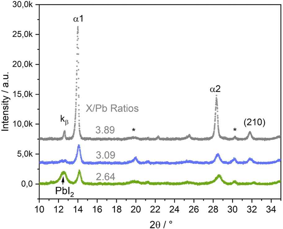 | ||
| Fig. 7 θ–θ scans of (Cs,FA)Pb(I,Br)3 layers with different X/Pb ratios (X = I + Br). I/Br ratios vary between 0.13 and 0.24, as listed in Table S1 in the ESI.† EDX spectra for each sample are shown in Fig. S12 and Fig. 8c in the ESI.† The * marks ITO peaks. | ||
Again, α1 and α2 peaks represent the (100) and (200) peaks of the perovskite α phase, respectively. α-(210) also correspond to the α phase, while PbI2 indicates the phase's (001) peak. At medium and high X/Pb no PbI2 or PbBr2 residues are visible. With increasing X/Pb, the α1, α2, and (210) peak areas increase, indicating an increase of the share of perovskite in the layer. The α1 peak area is highest for the sample with highest X/Pb. The peak at 12.7 corresponds to the α1 Kβ peak. While there is a large PbI2 peak visible in the sample with low X/Pb, no δFA peak can be observed, indicating a full suppression of the δ phase even for low X/Pb ratios. No PbBr2 peak was observed, suggesting preferential incorporation of Br for perovskite growth.
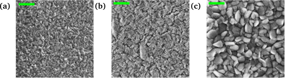
At even smaller X/Pb ratios, small peaks corresponding to the δ phase could be observed. An example for a layer with X/Pb of 2.54 can be found in Fig. S21 in the ESI.† This means that inclusion of Br does not generally lead to a complete δ suppression, but substantially lowers the AX content limit, at which the δ phase can be suppressed. This is a clear difference in comparison to the samples without Br, where the δFA peak was observed at I/Pb ratios of up to 3.6 (Fig. 4b). The SEM images of samples with Br are conclusive. At low X/Pb, supposedly PbI2 platelets surrounded by the smallest perovskite crytallites with slim, long shapes are grown. Although lighter spots, that can indicate PbX2 rich domains in the previously discussed SEM images in Fig. 3a and 6a, were visible, no such dominant segregation between PbX2 rich and perovskite phases was seen without Br. This could hint to a stronger tendency towards perovskite growth, when Br is included, thus modifying the lattice parameters and making intergrowth of perovskite and PbX2 rich phases less likely. At medium X/Pb in Fig. 8b, the average crystallite sizes increase considerably as they take round, pillar-like shapes. At highest X/Pb, the surface consists only of large grains and appears to be smoothed by the coverage of organic excess (Fig. S24 in the ESI†). The organic excess becomes apparent when considering the dark pinholes in Fig. 8c, that appear after several seconds of irradiation by the electron beam in organic rich layers.52,56
 | ||
| Fig. 8 (Cs,FAnPb(I,Br)2+n) samples with X/Pb ratios of 2.64 (a), 3.09 (b) and 3.89 (c) and Br/I ratios of 0.2, 0.24 and 0.13, respectively. Detailed EDX data are presented in Table S1 in the ESI.† The scalebar represents 500 nm. | ||
4 Discussion
We have observed stoichiometry-dependent trends in the preferential phase distribution during the growth of formamidinium-based perovskites and evaluated these trends along the X/Pb, Cs/FA and Br/I axes. In the following discussion, for simplicity, we will not discuss FAPbI3 and (Cs,FA)PbI3 separately.In our experiments a clear correlation between the perovskite growth and the AX/PbX2 ratio was found, with increasing crystallite sizes and an increasing relative content of the α perovskite phase share for an excess of AX. This phenomenon has been observed for wet-chemical24,44 as well as evaporated FAPbI345 and (Cs,FA)Pb(I,Br)38 layers, but up to now, only superficial explanations have been proposed for this mechanism including the creation of interstitial defects23 or defect and surface passivation44 similar to the effect that large organic cations have.21 Even though degradation mechanisms10,11,57–59 of FAPbI3 α to δ phase are well explored, to the best of our knowledge, no calculations or theories explaining the simultaneous growth of α and δ phases of FAPbI3 exist.
In a stoichiometric absorber, the FAPbI3 δ phase is favored at room temperature due to the oversized FA+ cation, as has been shown by many groups.47,60–63 Yet, freshly grown layers often contain large shares of the α phase and this share is increased by including a larger amount of A-cations.
A possible explanation for the observed co-existence could be local compositional deviations, as has been shown to occur for mixed-halide-64 and mixed-cation-perovskites.65 During co-evaporation, local compositional deviations could result from island-like growth-behaviour due to an increased adsorption coefficient at certain surfaces,66,67e.g. favoring FAI rich growth where FAI is already present at the surface. This would lead to crystallites with different AX/PbX2 ratios and thus potentially to different preferential crystal phases.
The question remains how the composition impacts the tendency of the material to grow in one phase or the other. Oner et al. investigated surface energy and defect formation energy caused by different types of surface-terminations in α FAPbI3 and found FAI-terminated surfaces to be the most energetically favorable and resilient to defect formation, more so than PbI2-terminated ones.68 An excess of FAI could therefore inhibit the formation of unfavorable defects and decrease the formation energy for α FAPbI3. A similar effect has been calculated to occur for iPAmH+2/15FAI14/15PbI46/15,60 where the formation energy for the α phase was decreased below the value for the δ phase by overstoichiometric addition of the large cation. We speculate, that surface passivation and defect formation resulting from FAI excess and consequently including the FA+ and I− ions could be less favorable in the δ phase than in the α phase. These defects could include theoretically predicted I3− trimers,61 interstitials FAi and Ii or the antisite defect FAPb, resulting in a stretched scaffold, large enough to hold FA+ cations due to reduced surface stress. The decrease in lattice constant in Fig. S17 and S19 in the ESI† likely also points in this direction.
The incorporation of Br in combination with Cs significantly stabilized the growth of the (Cs,FA)PbI3 α phase even for low Br/I in our experiments. This can be ascribed to a strong reduction of lattice strain in the (111) direction in FAPbI3 by the additional components.69 Amongst others, Zheng et al. observed a similar structural stabilization of FAPbI3 with MABr and assigned the beneficial effects to a more compact lattice by the smaller A cation and halide.15
In general terms, we investigated the phase relations of polymorphic FA-based perovskite thin films and their preference to grow in the desired, photo-active α perovskite phase along three parameter axes: the X/Pb ratio, the Cs/FA ratio and the I/Br ratio. While the incorporation of Br successfully suppressed the growth of the photo-inactive δ phase, the incorporation of Br will also significantly impact the bandgap, and might not be desired in all applications. Contrary to our expectations, the Cs/FA variation did not significantly impact the segregation of δ domains in the film. However, a strong impact of the X/Pb ratio on the α/δ relation was observed. As a consequence, special attention has to be paid to the X/Pb ratio in vacuum-based deposition of FA-based perovskites (and perovskites in general).
Nevertheless, in our contribution, we solely investigated the impact on the crystal lattice and phase relations. Obviously, the X/Pb ratio also strongly affects the opto-electronic properties,47,70 charge carrier densities71 and stability of the films, which also has to be taken into account for a complete solar cell device optimization. This has proven to be a complex task and seems to depend on several yet unknown factors. E.g., Chiang et al. found an optimized efficiency for evaporated (Cs,FA)Pb(I,Br)3 solar cells at an X/Pb ratio of 2.95, reducing crystallinity, but improving long-term structural stability by the excess of PbI2 in the layer.29 Ma et al. concluded excess PbI2 to be beneficial, but also observed increasing efficiency over time via degradation to PbI2 and resulting passivation.72 Cho et al. investigated (Cs,FA,MA)Pb(I,Br)3 solar cells and found the optimum X/Pb ratio to be at about 3.4, noticing an enhanced optical and cell stability for overstoichiometric samples,71 while Roß et al. produce FAPbI3 solar cells with PbI2 and FAI excess, respectively, showing similar efficiencies. In a more general approach it was shown, that unreacted PbI2 is detrimental for (Cs,FA,MA)Pb(I,Br)3 solar cells,40 hinting towards a natural benign effect of A-cation excess in perovskite absorbers. According to several groups, the effect of X/Pb at specific interfaces has to be considered, where PbI2 is beneficial at the ETL interface51,73,74 and A-cations at the HTL interface.73,75
5 Conclusions
In summary, we investigated the influence of compositional variations on the growth of FAnPbI2+n and double-cations (Cs,FA)nPbI2+n as well as (Cs,FA)nPb(I,Br)2+n perovskites and the occurence of possible secondary phases at room temperature. The results from our systematic study show consistently, that it is possible to preferentially grow the α phase and suppress the δ phase for all absorber types when the AX/PbX2 cation ratio is high enough. Without Cs, the threshold for suppression was found to be between I/Pb ratios of 3 to 3.9 The incorporation of Cs reduced the threshold to 3.6. However, solely through the introduction of Cs, the δ phase could not be completely suppressed for stoichiometric absorbers.Apart from the preferential α phase growth at higher I/Pb ratios, the respective peak intensities increased while the FWHM decreased and the observed crystallite sizes increased. The introduction of Br strongly enhanced the suppression of the δ phase even for smaller AX/PbX2 ratios. The threshold for δ phase suppression was then substantially reduced to a AX/PbX2 ratio of 2.6, showing the potential of α phase stabilization by mixing halides. These results lead to three generalized design rules for the preferential growth of the α phase in formamidinium-based lead halide perovskites: (i) FAI-rich synthesis; (ii) small beneficial effect due to the incorporation of CsI (iii) strong impact upon the addition of the smaller halide anion Br.
Author contributions
K. H. and P. W. prepared samples and collected and analyzed the experimental data equally, while P. P. guided the experimental work. M. M. provided additional PL measurements. R. S. and P. P. provided structural guidance, valuable discussions and important input. K. H. and P. P. composed the mansucript. All authors redacted and discussed the manuscript.Conflicts of interest
The authors have no conflicts of interest to declare.Acknowledgements
The authors are grateful for the high quality substrates provided by Thomas Richter. Financial support provided by the German Federal Ministry of Research and Education (BMBF) under contract number 03EK3570B (StrukturSolar II) is gratefully acknowledged. P. P. acknowledges funding by the Spanish Ministry of Universities under the Beatriz Galindo Senior program (BG20/00194).References
- A. Kojima, K. Teshima, Y. Shirai and T. Miyasaka, J. Am. Chem. Soc., 2009, 131, 6050–6051 CrossRef CAS PubMed.
- NREL, Best Research-Cell Efficiency Chart, 2022, https://www.nrel.gov/pv/cell-efficiency.html, Library Catalog: http://www.nrel.gov.
- Y.-H. Kim, S. Kim, A. Kakekhani, J. Park, J. Park, Y.-H. Lee, H. Xu, S. Nagane, R. B. Wexler, D.-H. Kim, S. H. Jo, L. Martínez-Sarti, P. Tan, A. Sadhanala, G.-S. Park, Y.-W. Kim, B. Hu, H. J. Bolink, S. Yoo, R. H. Friend, A. M. Rappe and T.-W. Lee, Nat. Photonics, 2021, 15, 148–155 CrossRef CAS.
- M. J. Bækbo, O. Hansen, I. Chorkendorff and P. C. K. Vesborg, RSC Adv., 2018, 8, 29899–29908 RSC.
- B. Conings, J. Drijkoningen, N. Gauquelin, A. Babayigit, J. D'Haen, L. D'Olieslaeger, A. Ethirajan, J. Verbeeck, J. Manca, E. Mosconi, F. D. Angelis and H.-G. Boyen, Adv. Energy Mater., 2015, 5, 1500477 CrossRef.
- B. C. ORegan, P. R. F. Barnes, X. Li, C. Law, E. Palomares and J. M. Marin-Beloqui, J. Am. Chem. Soc., 2015, 137, 5087–5099 CrossRef CAS.
- S. Li, Z. Liu, Z. Qiao, X. Wang, L. Cheng, Y. Zhai, Q. Xu, Z. Li, K. Meng and G. Chen, Adv. Funct. Mater., 2020, 2005846 CrossRef CAS.
- R. Ji, Z. Zhang, C. Cho, Q. An, F. Paulus, M. Kroll, M. Löffler, F. Nehm, B. Rellinghaus, K. Leo and Y. Vaynzof, J. Mater. Chem. C, 2020, 8, 7725–7733 RSC.
- S.-H. Turren-Cruz, A. Hagfeldt and M. Saliba, Science, 2018, 362, 449–453 CrossRef CAS PubMed.
- E. J. Juarez-Perez, L. K. Ono and Y. Qi, J. Mater. Chem. A, 2019, 7, 16912–16919 RSC.
- S. Thampy, B. Zhang, J.-G. Park, K.-H. Hong and J. W. P. Hsu, Mater. Adv., 2020, 1, 3349–3357 RSC.
- M. P. U. Haris, S. Kazim, M. Pegu, M. Deepa and S. Ahmad, Phys. Chem. Chem. Phys., 2021, 23, 9049–9060 RSC.
- A. Binek, F. C. Hanusch, P. Docampo and T. Bein, J. Phys. Chem. Lett., 2015, 6, 1249–1253 CrossRef CAS PubMed.
- N. Pellet, P. Gao, G. Gregori, T.-Y. Yang, M. K. Nazeeruddin, J. Maier and M. Grätzel, Angew. Chem., Int. Ed., 2014, 53, 3151–3157 CrossRef CAS PubMed.
- X. Zheng, C. Wu, S. K. Jha, Z. Li, K. Zhu and S. Priya, ACS Energy Lett., 2016, 1, 1014–1020 CrossRef CAS.
- Z. Li, M. Yang, J.-S. Park, S.-H. Wei, J. J. Berry and K. Zhu, Chem. Mater., 2016, 28, 284–292 CrossRef CAS.
- J.-W. Lee, D.-H. Kim, H.-S. Kim, S.-W. Seo, S. M. Cho and N.-G. Park, Adv. Energy Mater., 2015, 5, 1501310 CrossRef.
- B. Charles, M. T. Weller, S. Rieger, L. E. Hatcher, P. F. Henry, J. Feldmann, D. Wolverson and C. C. Wilson, Chem. Mater., 2020, 32, 2282–2291 CrossRef CAS.
- M. Saliba, T. Matsui, K. Domanski, J.-Y. Seo, A. Ummadisingu, S. M. Zakeeruddin, J.-P. Correa-Baena, W. R. Tress, A. Abate, A. Hagfeldt and M. Grätzel, Science, 2016, 206–209 CrossRef CAS PubMed.
- C. Shen, Y. Wu, S. Zhang, T. Wu, H. Tian, W.-H. Zhu and L. Han, Solar RRL, 2020, 4, 2000069 CrossRef CAS.
- Z. Zhang, R. Ji, M. Kroll, Y. J. Hofstetter, X. Jia, D. Becker-Koch, F. Paulus, M. Löffler, F. Nehm, K. Leo and Y. Vaynzof, Adv. Energy Mater., 2021, 11, 2100299 CrossRef CAS.
- Q. Ma, S. Huang, S. Chen, M. Zhang, C. F. J. Lau, M. N. Lockrey, H. K. Mulmudi, Y. Shan, J. Yao, J. Zheng, X. Deng, K. Catchpole, M. A. Green and A. W. Y. Ho-Baillie, J. Phys. Chem. C, 2017, 121, 19642–19649 CrossRef CAS.
- P. Becker, J. A. Márquez, J. Just, A. Al-Ashouri, C. Hages, H. Hempel, M. Jošt, S. Albrecht, R. Frahm and T. Unold, Adv. Energy Mater., 2019, 9, 1900555 CrossRef.
- Z. Yuan, Y. Miao, Z. Hu, W. Xu, C. Kuang, K. Pan, P. Liu, J. Lai, B. Sun, J. Wang, S. Bai and F. Gao, Nat. Commun., 2019, 10, 2818 CrossRef PubMed.
- M. Saliba, T. Matsui, J.-Y. Seo, K. Domanski, J.-P. Correa-Baena, M. Khaja Nazeeruddin, S. M. Zakeeruddin, W. Tress, A. Abate, A. Hagfeldt and M. Grätzel, Energy Environ. Sci., 2016, 9, 1989–1997 RSC.
- S. K. Yadavalli, Z. Dai, M. Hu, Q. Dong, W. Li, Y. Zhou, R. Zia and N. P. Padture, Acta Mater., 2020, 193, 10–18 CrossRef CAS.
- H. Min, M. Kim, S.-U. Lee, H. Kim, G. Kim, K. Choi, J. H. Lee and S. I. Seok, Science, 2019, 366, 749–753 CrossRef CAS.
- J. Borchert, R. L. Milot, J. B. Patel, C. L. Davies, A. D. Wright, L. Martínez Maestro, H. J. Snaith, L. M. Herz and M. B. Johnston, ACS Energy Lett., 2017, 2, 2799–2804 CrossRef CAS.
- Y.-H. Chiang, M. Anaya and S. D. Stranks, ACS Energy Lett., 2020, 5, 2498–2504 CrossRef CAS PubMed.
- J. Feng, Y. Jiao, H. Wang, X. Zhu, Y. Sun, M. Du, Y. Cao, D. Yang and S. F. Liu, Energy Environ. Sci., 2021, 14, 3035–3043 RSC.
- T. Burwig, K. Heinze and P. Pistor, Phys. Rev. Mater., 2022, 6, 065404 CrossRef CAS.
- L. Zhao, K. M. Lee, K. Roh, S. U. Z. Khan and B. P. Rand, Adv. Mater., 2019, 31, 1805836 CrossRef.
- D. Faiman, Prog. Photovoltaics Res. Appl., 2008, 16, 307–315 CrossRef CAS.
- H. Wang, X. Cheng and H. Yang, IEEE J. Photovolt., 2020, 10, 729–739 Search PubMed.
- N. Rolston, K. A. Bush, A. D. Printz, A. Gold-Parker, Y. Ding, M. F. Toney, M. D. McGehee and R. H. Dauskardt, Adv. Energy Mater., 2018, 8, 1802139 CrossRef.
- J. Zhao, Y. Deng, H. Wei, X. Zheng, Z. Yu, Y. Shao, J. E. Shield and J. Huang, Sci. Adv., 2017, 1–8 Search PubMed.
- B. Shi, X. Yao, F. Hou, S. Guo, Y. Li, C. Wei, Y. Ding, Y. Li, Y. Zhao and X. Zhang, J. Phys. Chem. C, 2018, 122, 21269–21276 CrossRef CAS.
- A. S. Yerramilli, Y. Chen, D. Sanni, J. Asare, N. D. Theodore and T. L. Alford, Org. Electron., 2018, 59, 107–112 CrossRef CAS.
- N. Ueoka and T. Oku, ACS Appl. Mater. Interfaces, 2018, 10, 44443–44451 CrossRef CAS PubMed.
- G. Tumen-Ulzii, C. Qin, D. Klotz, M. R. Leyden, P. Wang, M. Auffray, T. Fujihara, T. Matsushima, J.-W. Lee, S.-J. Lee, Y. Yang and C. Adachi, Adv. Mater., 2020, 32, 1905035 CrossRef CAS.
- F. Liu, Q. Dong, M. K. Wong, A. B. Djurišić, A. Ng, Z. Ren, Q. Shen, C. Surya, W. K. Chan, J. Wang, A. M. C. Ng, C. Liao, H. Li, K. Shih, C. Wei, H. Su and J. Dai, Adv. Energy Mater., 2016, 6, 1502206 CrossRef.
- R. Kottokkaran, H. A. Gaonkar, H. A. Abbas, M. Noack and V. Dalal, J. Mater. Sci.: Mater. Electron., 2019, 30, 5487–5494 CrossRef CAS.
- S.-Y. Hsiao, H.-L. Lin, W.-H. Lee, W.-L. Tsai, K.-M. Chiang, W.-Y. Liao, C.-Z. Ren-Wu, C.-Y. Chen and H.-W. Lin, Adv. Mater., 2016, 28, 7013–7019 CrossRef CAS.
- F. Ma, J. Li, W. Li, N. Lin, L. Wang and J. Qiao, Chem. Sci., 2017, 8, 800–805 RSC.
- M. Roß, L. Gil-Escrig, A. Al-Ashouri, P. Tockhorn, M. Jošt, B. Rech and S. Albrecht, ACS Appl. Mater. Interfaces, 2020, 12, 39261–39272 CrossRef.
- K. B. Lohmann, J. B. Patel, M. U. Rothmann, C. Q. Xia, R. D. J. Oliver, L. M. Herz, H. J. Snaith and M. B. Johnston, ACS Energy Lett., 2020, 5, 710–717 CrossRef CAS PubMed.
- M. Roß, S. Severin, M. B. Stutz, P. Wagner, H. Köbler, M. Favin-Lévêque, A. Al-Ashouri, P. Korb, P. Tockhorn, A. Abate, B. Stannowski, B. Rech and S. Albrecht, Adv. Energy Mater., 2021, 11, 2101460 CrossRef.
- S. Olthof and K. Meerholz, Sci. Rep., 2017, 7, 40267 CrossRef CAS.
- P. Pistor, J. Borchert, W. Fränzel, R. Csuk and R. Scheer, J. Phys. Chem. Lett., 2014, 5, 3308–3312 CrossRef CAS PubMed.
- T. Burwig, W. Fränzel and P. Pistor, J. Phys. Chem. Lett., 2018, 9, 4808–4813 CrossRef CAS PubMed.
- K. L. Heinze, O. Dolynchuk, T. Burwig, J. Vaghani, R. Scheer and P. Pistor, Sci. Rep., 2021, 11, 15299 CrossRef CAS PubMed.
- M. U. Rothmann, J. S. Kim, J. Borchert, K. B. Lohmann, C. M. OLeary, A. A. Sheader, L. Clark, H. J. Snaith, M. B. Johnston, P. D. Nellist and L. M. Herz, Science, 2020, 370, 1–7 CrossRef.
- J. Huang, P. Xu, J. Liu and X.-Z. You, Small, 2017, 13, 1603225 CrossRef.
- G. Murtaza and I. Ahmad, Phys. B: Condens. Matter, 2011, 406, 3222–3229 CrossRef CAS.
- D. H. Fabini, C. C. Stoumpos, G. Laurita, A. Kaltzoglou, A. G. Kontos, P. Falaras, M. G. Kanatzidis and R. Seshadri, Angew. Chem., 2016, 128, 15618–15622 CrossRef.
- J. Ran, O. Dyck, X. Wang, B. Yang, D. B. Geohegan and K. Xiao, Adv. Energy Mater., 2020, 10, 1903191 CrossRef CAS.
- P. Raval, R. M. Kennard, E. S. Vasileiadou, C. J. Dahlman, I. Spanopoulos, M. L. Chabinyc, M. Kanatzidis and G. N. Manjunatha Reddy, ACS Energy Lett., 2022, 1534–1543 CrossRef CAS.
- S. P. Dunfield, L. Bliss, F. Zhang, J. M. Luther, K. Zhu, M. F. A. M. van Hest, M. O. Reese and J. J. Berry, Adv. Energy Mater., 2020, 10, 1904054 CrossRef CAS.
- L. Ma, D. Guo, M. Li, C. Wang, Z. Zhou, X. Zhao, F. Zhang, Z. Ao and Z. Nie, Chem. Mater., 2019, 31, 8515–8522 CrossRef CAS.
- B.-w Park, H. W. Kwon, Y. Lee, D. Y. Lee, M. G. Kim, G. Kim, K.-j Kim, Y. K. Kim, J. Im, T. J. Shin and S. I. Seok, Nat. Energy, 2021, 6, 419–428 CrossRef CAS.
- A. Ruth, M. Holland, A. Rockett, E. Sanehira, M. D. Irwin and K. X. Steirer, Crystals, 2022, 12, 88 CrossRef CAS.
- C. Wu, K. Chen, D. Y. Guo, S. L. Wang and P. G. Li, RSC Adv., 2018, 8, 2900–2905 RSC.
- K. Nishimura, D. Hirotani, M. A. Kamarudin, Q. Shen, T. Toyoda, S. Iikubo, T. Minemoto, K. Yoshino and S. Hayase, ACS Appl. Mater. Interfaces, 2019, 11, 31105–31110 CrossRef CAS.
- C. G. Bischak, C. L. Hetherington, H. Wu, S. Aloni, D. F. Ogletree, D. T. Limmer and N. S. Ginsberg, Nano Lett., 2017, 17, 1028–1033 CrossRef CAS PubMed.
- R. Chatterjee, I. M. Pavlovetc, K. Aleshire, G. V. Hartland and M. Kuno, ACS Energy Lett., 2018, 3, 469–475 CrossRef CAS.
- L. I. Maissel, R. Glang and P. P. Budenstein, J. Electrochem. Soc., 1971, 118, 114C CrossRef.
- E. S. Parrott, J. B. Patel, A.-A. Haghighirad, H. J. Snaith, M. B. Johnston and L. M. Herz, Nanoscale, 2019, 11, 14276–14284 RSC.
- S. M. Oner, E. Sezen, M. S. Yordanli, E. Karakoc, C. Deger and I. Yavuz, J. Phys. Chem. Lett., 2022, 13, 324–330 CrossRef CAS PubMed.
- E. G. Moloney, V. Yeddu and M. I. Saidaminov, ACS Mater. Lett., 2020, 2, 1495–1508 CrossRef CAS.
- D. P. McMeekin, G. Sadoughi, W. Rehman, G. E. Eperon, M. Saliba, M. T. Hörantner, A. Haghighirad, N. Sakai, L. Korte, B. Rech, M. B. Johnston, L. M. Herz and H. J. Snaith, Science, 2016, 351, 151–155 CrossRef CAS PubMed.
- S. H. Cho, J. Byeon, K. Jeong, J. Hwang, H. Lee, J. Jang, J. Lee, T. Kim, K. Kim, M. Choi and Y. S. Lee, Adv. Energy Mater., 2021, 11, 2100555 CrossRef CAS.
- Z. Ma, D. Huang, Q. Liu, G. Yan, Z. Xiao, D. Chen, J. Zhao, Y. Xiang, C. Peng, H. Li, M. Zhang, W. Zhang, L. Duan and Y. Huang, J. Energy Chem., 2022, 66, 152–160 CrossRef CAS.
- J. Li, H. A. Dewi, H. Wang, J. Zhao, N. Tiwari, N. Yantara, T. Malinauskas, V. Getautis, T. J. Savenije, N. Mathews, S. Mhaisalkar and A. Bruno, Adv. Funct. Mater., 2021, 31, 2103252 CrossRef CAS.
- T. J. Jacobsson, J.-P. Correa-Baena, E. Halvani Anaraki, B. Philippe, S. D. Stranks, M. E. F. Bouduban, W. Tress, K. Schenk, J. Teuscher, J.-E. Moser, H. Rensmo and A. Hagfeldt, J. Am. Chem. Soc., 2016, 138, 10331–10343 CrossRef CAS PubMed.
- Z. Hu, Q. An, H. Xiang, L. Aigouy, B. Sun, Y. Vaynzof and Z. Chen, ACS Appl. Mater. Interfaces, 2020, 12, 54824–54832 CrossRef CAS PubMed.
Footnote |
| † Electronic supplementary information (ESI) available. See DOI: https://doi.org/10.1039/d2ma00507g |
| This journal is © The Royal Society of Chemistry 2022 |