
 Open Access Article
 This Open Access Article is licensed under a Creative Commons Attribution-Non Commercial 3.0 Unported Licence
Residual strain reduction leads to efficiency and operational stability improvements in flexible perovskite solar cells†
Sisi
He
 a,
Sibo
Li
b,
Anning
Zhang
a,
Guanshui
Xie
b,
Xin
Wang
b,
Jun
Fang
b,
Yabing
Qi
*c and
Longbin
Qiu
*b
a,
Sibo
Li
b,
Anning
Zhang
a,
Guanshui
Xie
b,
Xin
Wang
b,
Jun
Fang
b,
Yabing
Qi
*c and
Longbin
Qiu
*b
aFlexible Printed Electronics Technology Center, School of Science, Harbin Institute of Technology Shenzhen, Nanshan District, Shenzhen, Guangdong Province 518055, China
bSUSTech Energy Institute for Carbon Neutrality, Department of Mechanical and Energy Engineering, Southern University of Science and Technology, Shenzhen, 518055, China. E-mail: qiulb@sustech.edu.cn
cEnergy Materials and Surface Sciences Unit (EMSSU), Okinawa Institute of Science and Technology Graduate University (OIST), 1919-1 Tancha, Onna-son, Okinawa 904-0495, Japan. E-mail: Yabing.Qi@OIST.jp
First published on 24th June 2022
Abstract
Flexible perovskite solar cells (F-PSCs) hold promise for portable power sources for applications in various fields, such as wearable and portable electronics and lightweight power supply in stratosphere and space applications. To date, it is still a challenge to achieve efficient and stable F-PSCs. Herein, a pre-applied strain on a flexible substrate to release the residual strain of the perovskite layers of the F-PSCs is reported. As a result, the F-PSC based on this strategy yielded a power conversion efficiency (PCE) of up to 18.71%, approaching that of its counterpart based on a glass substrate (20.32%). And it retained 90% of its initial PCE after 300 h under AM 1.5G light illumination with an extrapolated T80 lifetime (the time over which the device efficiency reduces to 80% of its initial value) exceeding 700 h. Furthermore, the PCE remained above 80% of its initial value even after 1500 tension-only bending cycles. The result of this work paves a possible way toward fabricating efficient and stable F-PSCs.
1. Introduction
The remarkable progress in the development of metal halide perovskite solar cells (PSCs) in the past decade has been reflected by the rocketing power conversion efficiencies (PCEs) from the initial 3.8%1 to a certified 25.7%.2,3 The PSCs show a great potential in future solar energy applications with a theoretical efficiency of over 30%,4 which is higher than that of silicon solar cells with a theoretical limit of 29.1%.5 Furthermore, PSCs can potentially be integrated into a flexible format like a fiber structure,6 flexible thin film,7 or ultra-thin PSCs.8,9 As one of the boosting research directions in this promising photovoltaic technology, flexible PSCs (F-PSCs) have attracted enormous interest due to many apparent advantages including light weight, portability, compatibility with curved surfaces, ease of processing and reduced fabrication costs etc.10,11 In addition, F-PSCs demonstrate their energetic competition in contrast to other flexible photovoltaic technologies such as dye-sensitized solar cells12 and organic solar cells,13,14 showing great potential applications in various fields, such as wearable electronics, portable electronics and lightweight power supply in stratosphere and space applications, and unmanned aerial vehicles.11Great efforts have been exerted in the efficiency improvement of F-PSCs as the PCEs of F-PSCs are still lower than those of rigid-substrate-based PSCs.11,15 The effective improvement strategies of PSCs based on the rigid glass substrates, including engineering of transparent electrodes,16,17 optimization of each functional layer including electron transport layers (ETLs),18,19 perovskite layers,10,20 and counter electrodes,21 and interface engineering have been proposed to enhance the efficiency of F-PSCs. However, a flexible substrate exhibits different mechanical and thermal properties compared with a glass substrate. It is not always suitable to directly transfer these strategies based on a glass substrate to the flexible substrate. In addition, besides the high PCEs, stability poses a challenging yet rewarding issue towards the further commercialization and the achievement of the low-cost advantage in competition with other photovoltaic technologies.22 Therefore, more effort should be exerted to further improve the PCE of F-PSCs with high stability on flexible substrates.
Several optimization strategies have been investigated to address the current challenges for F-PSCs, e.g., flexible substrates with suitable mechanical properties, thermal resistance, and transparency; the coating of a uniform and high quality charge transport layer;23,24 the coating of a high-quality perovskite layer;15,25,26 grain boundary passivation;27 the encapsulation for stability; and structure design for mechanical bending.28 Several reports have recently achieved PCEs of over 18% and currently the record efficiency for F-PSCs is 21.1%9,25 and the operational stability under continuous light illumination is over 1000 h.24 A low-dimensional perovskite capping layer has been developed and coated for the passivation of grain boundaries and protection of the bottom perovskite films from breaking during bending.7 In other work, with the combination of an organic heterojunction on top of the perovskite layer, the light absorbance was extended to near-infrared and the resulting device showed an enhanced short-circuit current density (JSC) and a PCE to over 20% with a flexible format.29 Additive engineering is a readily available strategy to tune the nucleation and growth process for high quality perovskite and enhance the environmental resistance.30 Additive engineering has been applied for F-PSCs to show an efficiency of over 18.4%, which was the highest at the time reported.15 The incorporation of soft polymers such as polymethyl methacrylate (PMMA) and polyurethane (PU) into the perovskite layer could further enhance the flexibility and even stretchability of the as-coated perovskite layers and subsequently devices.31 The recently developed room temperature deposited hole transport layer VxNi1−xO further helped construct large area inverted structured flexible perovskite solar modules,32 which are expected to be more stable. On the other hand, the bending induced strain/stress of flexible electronics is an important topic. For a thin film device, during the mechanical bending process, there will be instant tensile (compressive) strain/stress in the upper (bottom) surface. With the release of the bend, the induced instant strain/stress will be also released. However, somewhere in between the top and bottom surface of the thin film device, the bending induced tensile (compressive) strain/stress will be zero, which is called the neutral plane.11,17 The position of the neutral plane is determined by the thickness and modulus of each layer within the thin film device. For F-PSCs, positioning the active layer in the neutral plane could reduce or eliminate the instant mechanical stress and strain during bending. A mechanical strain free F-PSC has been achieved by the selection of suitable encapsulation layers with appropriate thickness and modulus.11,17 However, as a main issue for F-PSCs, the residual constant stress/strain induced from the coating process has not been studied yet. And the residual strain is critical to carrier transport and collection, which will influence the device performance and also the stability.33–35
Herein, we report a strategy with pre-applied compressive strain on a flexible substrate surface to fabricate residual strain-free F-PSCs based on polyethylene naphthalate (PEN)/ITO. The crystal growth expansion and mismatched mechanical properties between the substrate and the perovskite layer induce the bulk residual strain for the resulting active film. The gradient strain of the perovskite layer on the flexible substrate has been reduced by designing a specific coating strategy to induce a pre-applied strain of the substrate. Combined with the optimization of the bottom SnO2 layer and passivation of the strain free perovskite layer with the PEAI, a champion PCE of 18.71% for the F-PSC has been obtained. The F-PSC showed high operational stability, retained 90% of its initial value under continuous AM 1.5G light illumination, and had an extrapolated T80 lifetime (the time over which the device efficiency reduces to 80% of its initial value) exceeding 700 h. Furthermore, the residual strain free F-PSC showed high mechanical flexibility, which retained 80% of its performance after 1500 tension-only bending cycles.
2 Results and discussion
The substrate and the coated perovskite layer show different coefficients of thermal expansion for the CH(NH2)2PbI3 (FAPbI3) (0.39 to 0.77 × 10⁻⁴ K−1),36,37 the ITO (0.37 to 1 × 10⁻⁵ K−1)35 and glass substrate (6.7 × 10⁻⁷ K−1) or PEN (10−6 K−1);38 thus a strain will be induced or released for the perovskite layer under the heating process or light illumination.36,39,40 It has been shown that due to the larger thermal expansion coefficient of perovskite, a compressive strain will occur on the top of the perovskite layer after cooling.41 However, there are also reports showing that there is tensile strain on top of the coated perovskite layer, which is caused by the gradient thermal annealing and the tensile strain could be released by an upside down annealing or surface post-treatment.33,34 It has been shown that in a two-step deposition process, the crystal expands from PbI2 to the perovskite structure with the thickness increase with a ratio of two.42 We propose that this expansion might also happen for one-step deposition from the precursor with PbI2 and organic salt. And the expansion may be a cause for the surface tensile strain (Fig. 1a). Due to the strong interface interaction between the perovskite precursor and substrate, there will be compressive strain in the interface during the crystal growth with volume expansion, which will induce a tensile strain on the top surface. And we proposed that with a pre-applied compressive strain on the surface substrate, a crystal growth induced residual strain might be released/reduced, as shown in Fig. 1b and c.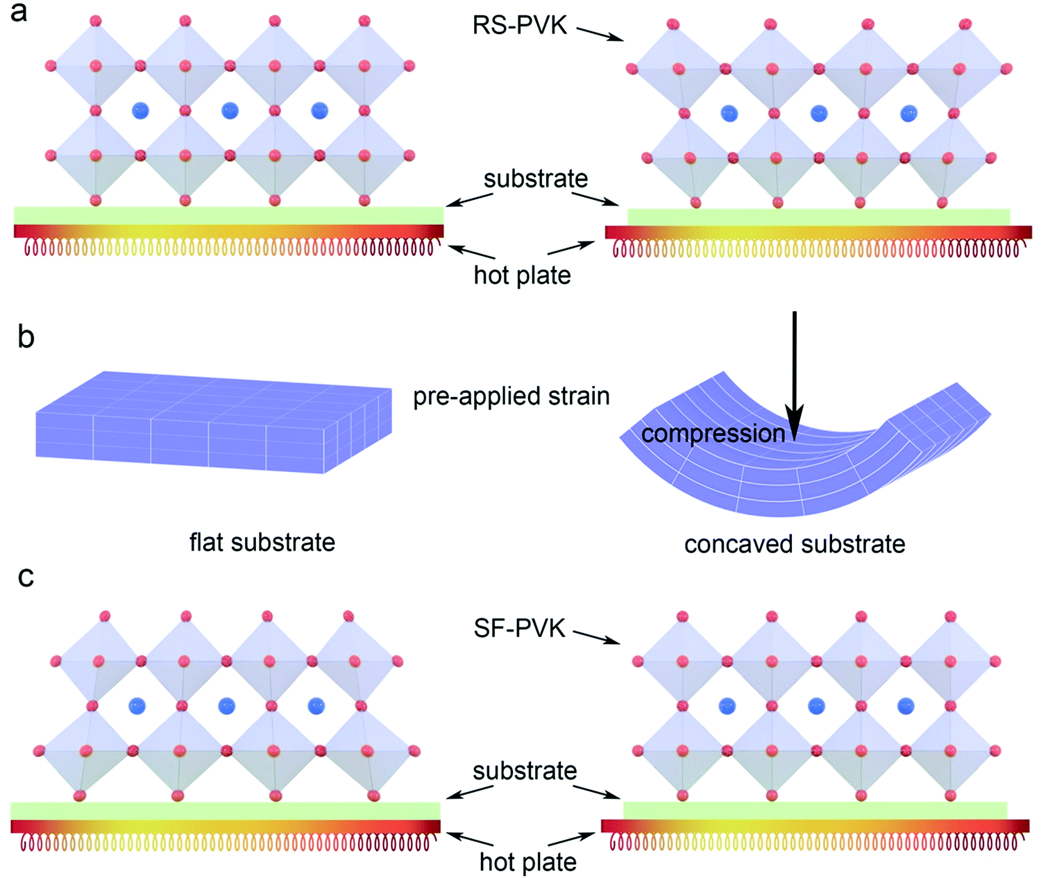 | ||
| Fig. 1 Schematic drawing showing (a) the formation of residual strain perovskite (RS-PVK) on a flat substrate; (b) the pre-applied compressive strain on a concave substrate (the mesh is indicated to show the strain on the substrate); and (c) the formation of strain free (SF-PVK) on a concave substrate. | ||
To explore whether there is induced tensile or compressive strain of the perovskite film on the flexible substrate, we conducted grazing incident X-ray diffraction (GIXRD) measurements to estimate the residual strain at different depths of the perovskite films.43 During the measurement of residual strain at a specific depth, a specific incident angle should be chosen and fixed by gradually tuning the instrument tilt angle ψ.43 Initially, the perovskite layer was spin coated on a flat surface, by attaching the flexible substrate on top of a rigid plate. The perovskite films on the substrate showed XRD peaks at 2θ around 14° and 31.6° corresponding to (001) and (012) crystallographic planes, respectively (Fig. 2a and b).33 Here, we chose the diffraction angle of the (012) plane due to its high diffraction angle and smaller influence of the substrate and the obtained XRD patterns are shown in Fig. 2c.33 By tuning ψ from 0 to 45°, the diffraction peaks gradually shifted to a smaller degree for the flat perovskite film.33 It indicates that there was a residual tensile strain along the horizontal direction in the perovskite film. Here, we call it the residual-strain perovskite film (RS-PVK). Furthermore, at a deeper incident depth, the tensile strain decreased. From the GIXRD data we found that in the vertical direction crystal plane distance is smaller in the top surface than in the bottom interface (Fig. 2d), which indicated a compression in the interface between perovskite/SnO2. And due to the compression in the bottom interface, there will be a small expansion on the top surface in the horizontal direction (Fig. 2f).
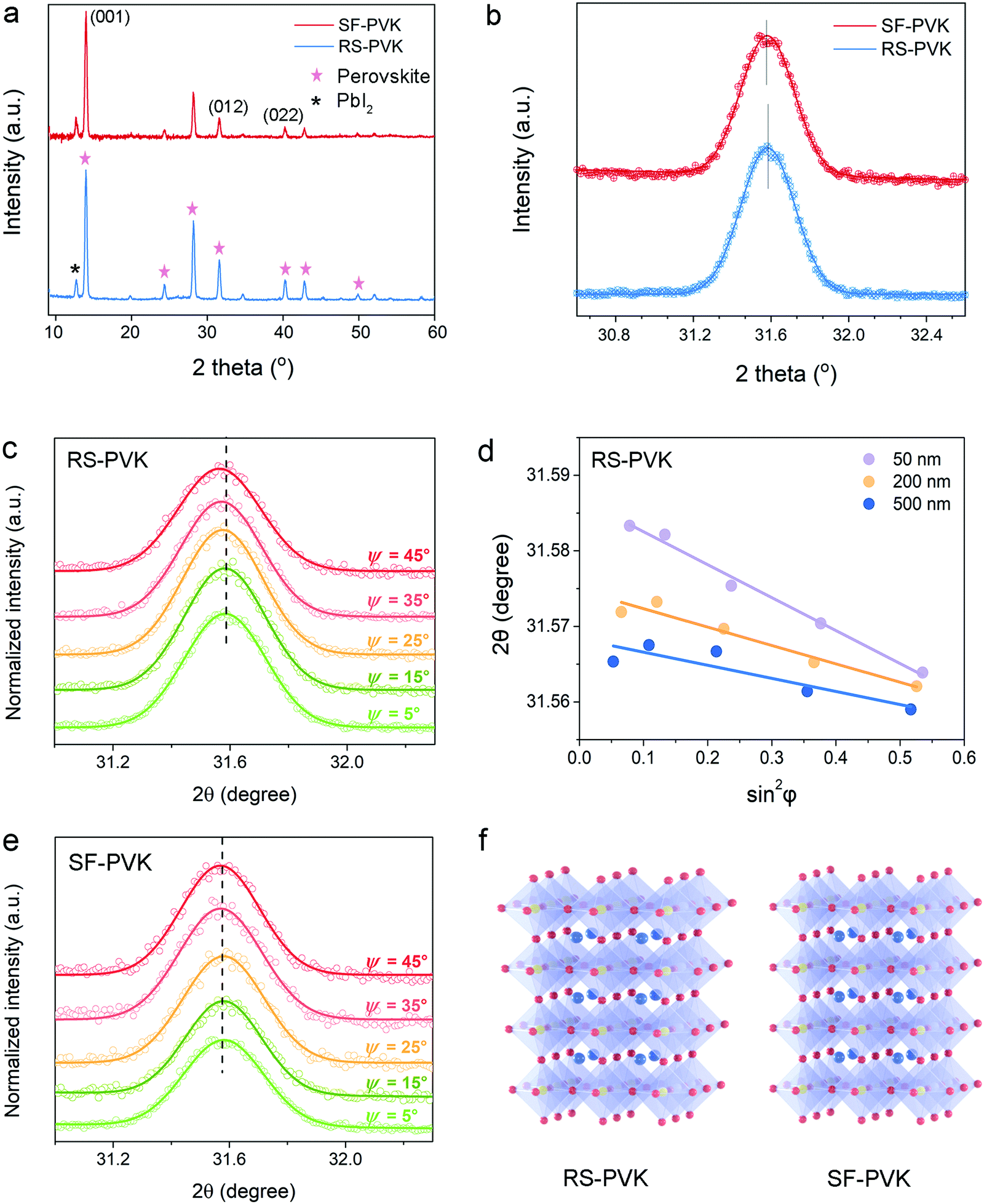 | ||
| Fig. 2 (a) GIXRD spectra and (b) enlarged (012) plane of the SF-PVK and RS-PVK fabricated on the PEN/ITO flexible substrate. (c) GIXRD spectrum at a depth of 50 nm with different tilt angles for the perovskite coated on a flat flexible substrate (RS-PVK). (d) The gradient strain of perovskite layers, where the top surface has the highest residual strain. (e) GIXRD at a depth of 50 nm with different tilt angles for SF-PVK. (f) Schematic drawing showing the perovskite structure with (RS-PVK) and without (SF-PVK) gradient strain. | ||
To release the residual strain of the perovskite film on flexible substrates, strain engineering was applied during the preparation process of the perovskite film. We fabricated perovskite films with pre-applied strains by reshaping the PEN/ITO substrate with a concave shape by putting the PEN/ITO substrate on a rotating head of the spin coater containing a pumping hole (Fig. S1, ESI†). To get more and deeper understanding regarding the change of grain lattice of perovskite, GIXRD measurements with different incident angles were performed. As expected, the diffraction peaks showed no obvious change for the concaved perovskite film by tuning ψ from 0 to 45° (Fig. 2e). After applying a pre-strain on the concave substrate during the fabrication of the perovskite film, the residual strain and strain gradient were reduced (Fig. S2, ESI†). For simplicity, we call it the strain-free perovskite film (SF-PVK).
To further study the pre-applied strain reducing the residual strain during the coating process, the perovskite layers were coated on substrates with different concave degrees. The degree of concave substrates can be modified by using O-rings of different diameters for spin coating (Fig. S3, ESI†). The maximum displacement of the substrate bottom surface was defined as the degree of concave substrates (Table S1, ESI†). For a coating process after dropping the antisolvent, the perovskite precursor layer would be deposited on a substrate with/without pre-applied strain, with a strong interaction bonding to the SnO2.41 In this case, after the annealing and crystal growing process a perovskite layer with reduced strain was obtained (Fig. 1c). However, it will be difficult to coat uniform films on a substrate with a larger deformation. In this case, an O-ring with a 5.2 mm diameter was applied.
F-PSCs were fabricated based on the RS-PVK and SF-PVK, with the device configuration as shown in Fig. 3a. The perovskite layer was uniformly attached on the surface of the PEN/ITO/SnO2 film (Fig. 3b). On the other hand, to suppress the surface defects of perovskite films to achieve efficient solar cells, phenethylammonium iodide (PEAI) was applied for post-treatment and passivation.44 The X-ray photoelectron spectroscopy (XPS) measurements of the Pb 4f and I 3d core-level energy spectra (Fig. S4, ESI†) indicated the presence of a higher ratio of iodide on the perovskite surface and that the iodine vacancy is likely to be filled, which is consistent with the previous report.44 PSCs on a rigid glass substrate have been fabricated as comparison and a champion PCE of 20.32% for the PSC on glass substrate is obtained with an open-circuit voltage (VOC) of 1.08 V, a JSC of 24.26 mA cm−2 and a fill factor (FF) of 77.2% (Fig. S5, ESI†). It has been shown that the flexible substrate has a reduced light transmittance especially in the range below 390 nm wavelength, i.e., UV light through the PEN/ITO substrate (Fig. S6, ESI†). This property may improve the stability of the F-PSCs as the irradiation of UV can cause the degradation of perovskite materials45 while the rigid glass/ITO substrate has a lower surface roughness (Fig. S7a and b, ESI†). It has been reported that with a smooth surface and a suitable thickness of SnO2, the transmittance of the PEN/ITO/SnO2 substrate could be much improved (Fig. S7c and d, ESI†).18 The increased transmittance may come from the gradient n values of air (1), PEN (∼1.5), ITO (∼1.8), and SnO2 (∼2.3), due to the interference between the reflected light from the ITO/SnO2 and SnO2/air interfaces.18 On the other hand, with the increased thickness of SnO2, a smoother and a compact surface was obtained. It has been proposed that the smoother surface is beneficial for light transmission.46 We further confirmed that with a suitable thickness of SnO2 the flexible substrate shows the highest transmittance.
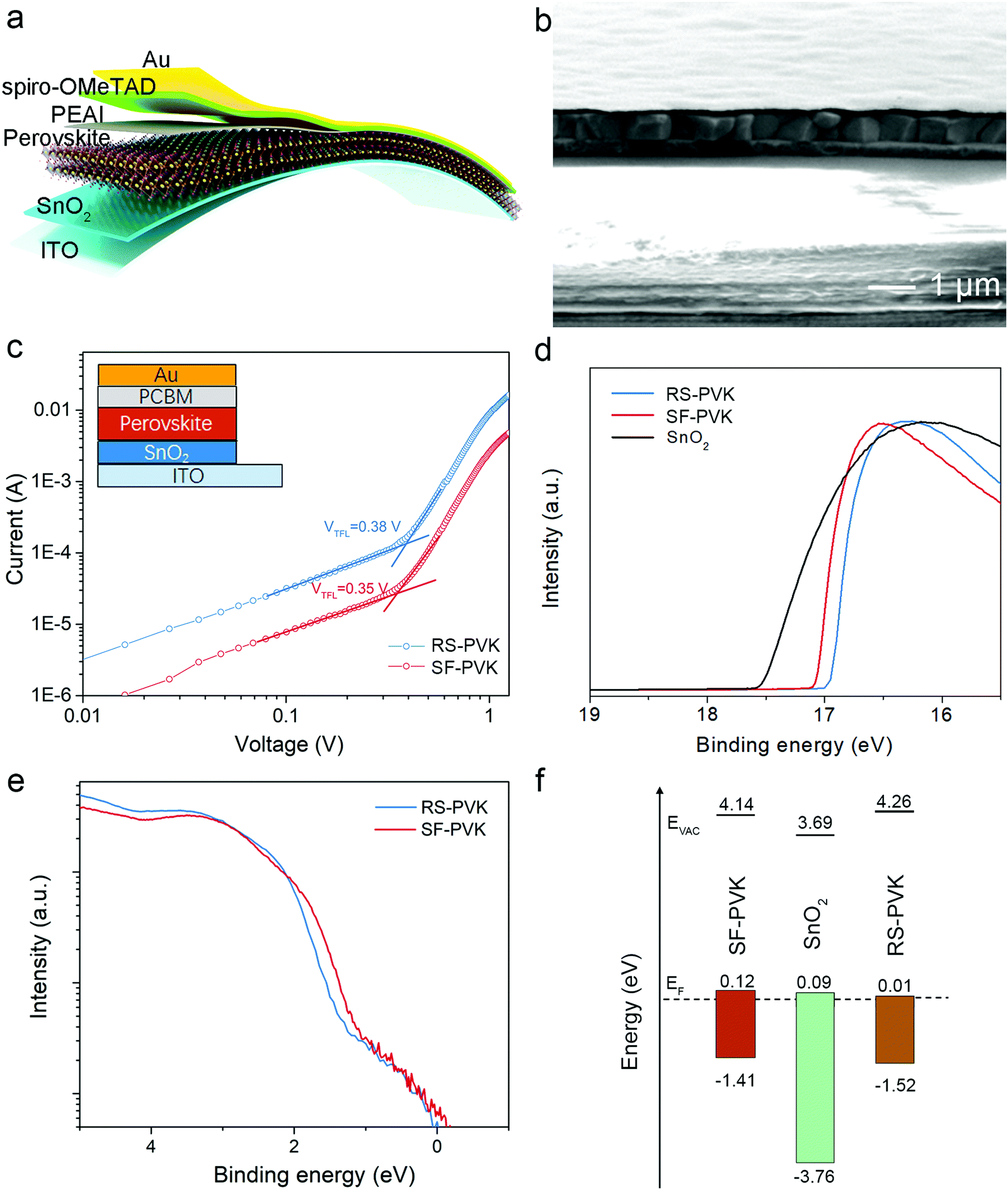 | ||
| Fig. 3 (a) Schematic drawing showing the device configuration for the F-PSCs. (b) Cross-sectional SEM image of the F-PSCs. (c) Dark I–V curves of the electron-only devices with a structure of ITO/SnO2/perovskite/PCBM/Au made of SF-PVK and RS-PVK. (d) UPS spectra of the SF-PVK and RS-PVK (SF-PVK: WF = 4.14 eV; RS-PVK: WF = 4.26 eV). The SnO2 shows a WF of 3.69 eV. (e) The UPS valence band features of RS-PVK (1.52 eV) and SF-PVK (1.41 eV) on a semi-log scale. (f) The energy level diagram of F-PSCs based on RS-PVK and SF-PVK. | ||
With the combination of the optimization of ETL and the interface between perovskite and spiro-OMeTAD, the F-PSCs were fabricated. The photovoltaic performance of solar cells with different SnO2 thicknesses and PEAI passivation on flexible substrates was measured and the representative current density–voltage (J–V) curves are presented in Fig. S8 (ESI†) and the extracted photovoltaic parameters are summarized in Table S2 (ESI†). The performance first gradually increased with the increasing thickness of the SnO2 layer. The champion PSC with the optimum SnO2 thickness of 100 nm exhibits a PCE of 16.5%. With the further increase of the thickness of SnO2 to 125 nm, although the FF was further enhanced, both VOC and JSC decreased, resulting in the declined PCEs. Hence, we chose 100 nm as the thickness of SnO2 for the following investigation. To obtain a compact and thicker SnO2 layer on a flexible substrate, a higher concentration solution and repeated coating process was applied (ESI†). However, for SnO2 on a rigid glass substrate, the thickness is around 20 nm, due to better wettability and a smoother surface.47
For perovskite coated on a flat and curved substrate, the morphology did not show a distinguishable difference, while there are more smaller grains in the RS-PVK perovskite layer (Fig. S9, ESI†). The change of the crystal residual strain may influence the optoelectronic properties of the materials.33 Therefore, we investigated the trap densities of the RS-PVK and SF-PVK to reveal the influence of residual strain on the performance of F-PSCs by using the space charge limited current (SCLC) method. The dark current–voltage (I–V) characteristics of the electron-only device were obtained by building the architecture of ITO/SnO2/perovskite/PCBM/Au under dark conditions (Fig. 3c). At the low bias voltage, the current and the voltage showed a linear correlation, indicating an Ohmic response in this region. The current increases sharply when the bias voltage exceeds a specific voltage, which is called the trap-filling limit voltage (VTFL). In this trap-filling limited region, the trap states are filled. It shows that the VTFL of the SF-PVK is 0.35 V, which is lower than that of the RS-PVK (VTFL= 0.38 V). As the trap-state density has a linear correlation with the VTFL, it indicates that the trap-state density of the perovskite film decreased after the residual strain was released. The reduced trap-state density may contribute to the increased current density of the resultant PSCs.
The work function (WF) and valence band maximum changes of the perovskite with/without residual strain has been traced by employing ultraviolet photoemission spectroscopy (UPS), as shown in Fig. 3d and e. The WF of SnO2 is determined to be 3.69 eV, and the WF of the perovskite films decreased from 4.26 eV to 4.14 eV after the residual strain was released. The valence band maximum is determined to be 1.52 eV and 1.41 eV, respectively, yielding the ionization energy value of 5.78 eV and 5.55 eV for RS-PVK and SF-PVK (Fig. 3e). A higher VOC is expected with the better energy level alignment between the bottom SnO2 and SF-PVK (Fig. 3f).
To investigate the impact of the release of residual strain on the performance of F-PSCs, we measured the J–V performance of the devices based on SF-PVK and devices based on RS-PVKs as the control samples under a simulated illumination of AM 1.5G and 100 mW cm−2. The achieved best SF-PSC generated a PCE of 18.71% with a VOC of 1.02 V, a JSC of 23.91 mA cm−2 and a FF of 77.0% (Table 1). Meanwhile, there is negligible hysteresis between the forward and reverse scanning J–V curves (Fig. 4a). In comparison, the RS-PSCs tested under identical conditions showed a lower average PCE of 16.5% with the VOC of 1.02 V, JSC of 22.72 mA cm−2 and FF of 71.6%. It is found that JSC clearly improved after the application of pre-strain on the substrate during the fabrication process of the perovskite film. The higher current density of SF-PSCs was further proven by the external quantum efficiency (EQE) spectrum (Fig. 4b), showing a higher value along the entire absorption wavelength and a higher integrated JSC compared with that of RS-PSCs. And the average VOC was also enhanced after the release of residual stress in the perovskite film, as expected from the better energy level alignment. It suggests that the SF-PSCs show improved light harvesting efficiencies compared to the RS-PSCs due to the decreased trap densities, which is in good agreement with the SCLC data.
| Device type | Scan direction | V OC [V] | J SC [mA cm−2] | J SC (EQE) [mA cm−2] | FF [%] | PCE [%] |
|---|---|---|---|---|---|---|
| RS-PVK | Reverse | 0.98 ± 0.03 | 22.7 ± 0.1 | 22.1 | 71 ± 1 | 15.9 ± 0.5 |
| Forward | 0.96 ± 0.01 | 22.8 ± 0.1 | 69 ± 2 | 15.2 ± 0.1 | ||
| SF-PVK | Reverse | 1.03 ± 0.02 | 23.8 ± 0.1 | 22.8 | 75 ± 2 | 18.5 ± 0.2 |
| Forward | 1.03 ± 0.02 | 23.8 ± 0.2 | 74 ± 2 | 18.1 ± 0.2 |
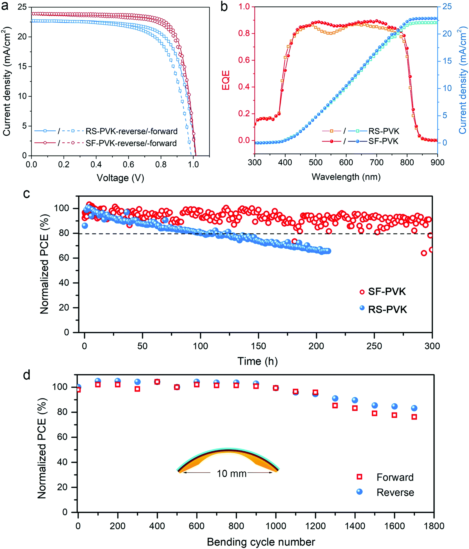 | ||
| Fig. 4 (a) Representative J–V curves of the PSCs made of SF-PVK and RS-PVK with forward and reverse scans. (b) Corresponding EQE spectra of the F-PSCs. (c) Operational stability of un-encapsulated F-PSCs with varying structures measured at a fixed bias near the maximum power point (MPP) under continuous illumination. (d) The PCEs of SF-PSCs as a function of bending cycles. | ||
To study whether the reduced residual strain on the perovskite layer can improve the stability of resultant F-PSCs, we measured the operation stability of the RS-PSCs and SF-PSCs. As shown in Fig. 4c, the PCE of SF-PSCs retained 90% of the initial value after more than 300 h with an extrapolated T80 lifetime exceeding 700 h under the continuous light illumination, which is much longer than the RS-PSC case (T80 ∼ 100 h). The stability of the F-PSCs was enhanced after the release of residual strain in the perovskite film. We further performed mechanical bending tests of F-PSCs to evaluate their bending resistance for their promising practical applications for instance in a wearable device as power suppliers. As displayed in Fig. 4d, the PCEs of SF-PSCs remained above 80% of the initial value even after 1500 bending cycles with a bending radius of 5 mm. The decreased performance after a long-time bending behavior might be due to the generated cracks, which could be seen in the PEN/ITO flexible substrates and their conductivity significantly reduced while for RS-PSCs, the performance decreased faster to remain below 80% of its initial value after 1200 bending cycles (Fig. S10, ESI†).
3. Conclusion
In conclusion, we have demonstrated a strategy for the release of the residual strain in the perovskite layer. The resultant F-PCSs based on the pre-applied strain strategy achieved a PCE of up to 18.71%. The F-PSCs maintained 90% of their initial performance after continuous operation for 300 h under AM 1.5G light illumination, which translates into a T80 lifetime exceeding 700 h. Moreover, the PCEs of F-PSCs retained above 80% of their initial value even after 1500 bending tests.Conflicts of interest
There are no conflicts of interest to declare.Acknowledgements
S. H. acknowledges the funding by National Natural Science Foundation of China (NSFC) (52103300) and the Shenzhen Science and Technology Program (JCYJ20210324132806017, KQTD20200820113045083). L. Q. acknowledges the funding by the NSFC (22109067), the Guangdong Provincial Science and Technology Program (2022A1515010085), and the research startup grant support by the Southern University of Science and Technology (SUSTech). The authors would also like to acknowledge the technical support from the SUSTech Core Research Facilities. Y. B. Q. acknowledges the support from the Energy Materials and Surface Sciences Unit of the Okinawa Institute of Science and Technology Graduate University.References
- A. Kojima, K. Teshima, Y. Shirai and T. Miyasaka, J. Am. Chem. Soc., 2009, 131, 6050 CrossRef CAS PubMed.
- H. Min, D. Y. Lee, J. Kim, G. Kim, K. S. Lee, J. Kim, M. J. Paik, Y. K. Kim, K. S. Kim, M. G. Kim, T. J. Shin and S. Il Seok, Nature, 2021, 598, 444 CrossRef CAS PubMed.
- M. A. Green, E. D. Dunlop, J. Hohl-Ebinger, M. Yoshita, N. Kopidakis and X. Hao, Prog. Photovolt. Res. Appl, 2022, 30, 3 CrossRef.
- N. G. Park and H. Segawa, ACS Photonics, 2018, 5, 2970 CrossRef CAS.
- K. Yoshikawa, H. Kawasaki, W. Yoshida, T. Irie, K. Konishi, K. Nakano, T. Uto, D. Adachi, M. Kanematsu, H. Uzu and K. Yamamoto, Nat. Energy, 2017, 2, 17032 CrossRef CAS.
- L. Qiu, J. Deng, X. Lu, Z. Yang and H. Peng, Angew. Chem., Int. Ed., 2014, 53, 10425 CrossRef CAS PubMed.
- Q. Dong, M. Chen, Y. Liu, F. T. Eickemeyer, W. Zhao, Z. Dai, Y. Yin, C. Jiang, J. Feng, S. Jin, S. Liu, S. M. Zakeeruddin, M. Grätzel, N. P. Padture and Y. Shi, Joule, 2021, 5, 1587 CrossRef CAS.
- M. Kaltenbrunner, G. Adam, E. D. Glowacki, M. Drack, R. Schwodiauer, L. Leonat, D. H. Apaydin, H. Groiss, M. C. Scharber, M. S. White, N. S. Sariciftci and S. Bauer, Nat. Mater., 2015, 14, 1032 CrossRef CAS PubMed.
- Y. Hu, T. Niu, Y. Liu, Y. Zhou, Y. Xia, C. Ran, Z. Wu, L. Song, P. Müller-Buschbaum, Y. Chen and W. Huang, ACS Energy Lett., 2021, 6, 2917 CrossRef CAS.
- M. Li, Y. G. Yang, Z. K. Wang, T. Kang, Q. Wang, S. H. Turren-Cruz, X. Y. Gao, C. S. Hsu, L. S. Liao and A. Abate, Adv. Mater., 2019, 31, e1901519 CrossRef PubMed.
- H. S. Jung, G. S. Han, N.-G. Park and M. J. Ko, Joule, 2019, 3, 1850 CrossRef CAS.
- M. Cai, Y. Wu, H. Chen, X. Yang, Y. Qiang and L. Han, Adv. Sci., 2017, 4, 1600269 CrossRef PubMed.
- M. Kaltenbrunner, M. S. White, E. D. Głowacki, T. Sekitani, T. Someya, N. S. Sariciftci and S. Bauer, Nat. Commun., 2012, 3, 770 CrossRef PubMed.
- H. Jinno, K. Fukuda, X. Xu, S. Park, Y. Suzuki, M. Koizumi, T. Yokota, I. Osaka, K. Takimiya and T. Someya, Nat. Energy, 2017, 2, 780 CrossRef CAS.
- J. Feng, X. Zhu, Z. Yang, X. Zhang, J. Niu, Z. Wang, S. Zuo, S. Priya, S. F. Liu and D. Yang, Adv. Mater., 2018, 30, e1801418 CrossRef PubMed.
- T. Zhu, Y. Yang, X. Yao, Z. Huang, L. Liu, W. Hu and X. Gong, ACS Appl. Mater. Interfaces, 2020, 12, 15456 CrossRef CAS PubMed.
- G. Lee, M.-c Kim, Y. W. Choi, N. Ahn, J. Jang, J. Yoon, S. M. Kim, J.-G. Lee, D. Kang, H. S. Jung and M. Choi, Energy Environ. Sci., 2019, 12, 3182 RSC.
- K. Huang, Y. Peng, Y. Gao, J. Shi, H. Li, X. Mo, H. Huang, Y. Gao, L. Ding and J. Yang, Adv. Energy Mater., 2019, 9, 1901419 CrossRef CAS.
- Q. Dong, J. Li, Y. Shi, M. Chen, L. K. Ono, K. Zhou, C. Zhang, Y. B. Qi, Y. Zhou, N. P. Padture and L. Wang, Adv. Energy Mater., 2019, 9, 1900834 CrossRef.
- X. Dai, Y. Deng, C. H. Van Brackle, S. Chen, P. N. Rudd, X. Xiao, Y. Lin, B. Chen and J. Huang, Adv. Energy Mater., 2019, 10, 1903108 CrossRef.
- J. Yoon, H. Sung, G. Lee, W. Cho, N. Ahn, H. S. Jung and M. Choi, Energy Environ. Sci., 2017, 10, 337 RSC.
- S. He, L. Qiu, L. K. Ono and Y. B. Qi, Mater. Sci. Eng., R, 2020, 140, 100545 CrossRef.
- J. Chung, S. S. Shin, K. Hwang, G. Kim, K. W. Kim, D. S. Lee, W. Kim, B. S. Ma, Y.-K. Kim, T.-S. Kim and J. Seo, Energy Environ. Sci., 2020, 13, 4854 RSC.
- Q. Dong, C. Zhu, M. Chen, C. Jiang, J. Guo, Y. Feng, Z. Dai, S. K. Yadavalli, M. Hu, X. Cao, Y. Li, Y. Huang, Z. Liu, Y. Shi, L. Wang, N. P. Padture and Y. Zhou, Nat. Commun., 2021, 12, 973 CrossRef CAS PubMed.
- L. Yang, Q. Xiong, Y. Li, P. Gao, B. Xu, H. Lin, X. Li and T. Miyasaka, J. Mater. Chem. A, 2021, 9, 1574 RSC.
- Z. Xing, S. Lin, X. Meng, T. Hu, D. Li, B. Fan, Y. Cui, F. Li, X. Hu and Y. Chen, Adv. Funct. Mater., 2021, 31, 2107726 CrossRef CAS.
- C. Ge, Z. Yang, X. Liu, Y. Song, A. Wang and Q. Dong, CCS Chem., 2021, 3, 2035 CrossRef CAS.
- X. Meng, Z. Cai, Y. Zhang, X. Hu, Z. Xing, Z. Huang, Z. Huang, Y. Cui, T. Hu, M. Su, X. Liao, L. Zhang, F. Wang, Y. Song and Y. Chen, Nat. Commun., 2020, 11, 3016 CrossRef CAS PubMed.
- S. Wu, Z. Li, J. Zhang, X. Wu, X. Deng, Y. Liu, J. Zhou, C. Zhi, X. Yu, W. C. H. Choy, Z. Zhu and A. K. Jen, Adv. Mater., 2021, 33, e2105539 CrossRef PubMed.
- A. Kotta, E.-B. Kim, I. Seo, Z. A. Ansari and H. K. Seo, Solar RRL, 2021, 5, 2100826 CrossRef CAS.
- X. Meng, Z. Xing, X. Hu, Z. Huang, T. Hu, L. Tan, F. Li and Y. Chen, Angew. Chem., Int. Ed., 2020, 59, 16602 CrossRef CAS PubMed.
- A. Kotta, I. Seo, H.-S. Shin and H.-K. Seo, Chem. Eng. J., 2022, 435, 134805 CrossRef CAS.
- C. Zhu, X. Niu, Y. Fu, N. Li, C. Hu, Y. Chen, X. He, G. Na, P. Liu, H. Zai, Y. Ge, Y. Lu, X. Ke, Y. Bai, S. Yang, P. Chen, Y. Li, M. Sui, L. Zhang, H. Zhou and Q. Chen, Nat. Commun., 2019, 10, 815 CrossRef CAS PubMed.
- H. Wang, C. Zhu, L. Liu, S. Ma, P. Liu, J. Wu, C. Shi, Q. Du, Y. Hao, S. Xiang, H. Chen, P. Chen, Y. Bai, H. Zhou, Y. Li and Q. Chen, Adv. Mater., 2019, 31, e1904408 CrossRef PubMed.
- J. Wu, S. C. Liu, Z. Li, S. Wang, D. J. Xue, Y. Lin and J. S. Hu, Natl. Sci. Rev., 2021, 8, nwab047 CrossRef CAS PubMed.
- T. J. Jacobsson, L. J. Schwan, M. Ottosson, A. Hagfeldt and T. Edvinsson, Inorg. Chem., 2015, 54, 10678 CrossRef CAS PubMed.
- T. Haeger, R. Heiderhoff and T. Riedl, J. Mater. Chem. C, 2020, 8, 14289 RSC.
- Y. Zoo, D. Adams, J. W. Mayer and T. L. Alford, Thin Solid Films, 2006, 513, 170 CrossRef CAS.
- H. Tsai, R. Asadpour, J.-C. Blancon, C. C. Stoumpos, O. Durand, J. W. Strzalka, B. Chen, R. Verduzco, P. M. Ajayan, S. Tretiak, J. Even, M. A. Alam, M. G. Kanatzidis, W. Nie and A. D. Mohite, Science, 2018, 360, 67 CrossRef CAS PubMed.
- J. J. Zhao, Y. H. Deng, H. T. Wei, X. P. Zheng, Z. H. Yu, Y. C. Shao, J. E. Shield and J. S. Huang, Sci. Adv., 2017, 3, eaao5616 CrossRef PubMed.
- W. Meng, K. Zhang, A. Osvet, J. Zhang, W. Gruber, K. Forberich, B. Meyer, W. Heiss, T. Unruh, N. Li and C. J. Brabec, Joule, 2022, 6, 458 CrossRef CAS.
- L. Qiu, S. He, Y. Jiang, D.-Y. Son, L. K. Ono, Z. Liu, T. Kim, T. Bouloumis, S. Kazaoui and Y. B. Qi, J. Mater. Chem. A, 2019, 7, 6920 RSC.
- J. Peng, V. Ji, W. Seiler, A. Tomescu, A. Levesque and A. Bouteville, Surf. Coat. Technol., 2006, 200, 2738 CrossRef CAS.
- Q. Jiang, Y. Zhao, X. W. Zhang, X. L. Yang, Y. Chen, Z. M. Chu, Q. F. Ye, X. X. Li, Z. G. Yin and J. B. You, Nat. Photonics, 2019, 13, 460 CrossRef CAS.
- S.-W. Lee, S. Kim, S. Bae, K. Cho, T. Chung, L. E. Mundt, S. Lee, S. Park, H. Park, M. C. Schubert, S. W. Glunz, Y. Ko, Y. Jun, Y. Kang, H.-S. Lee and D. Kim, Sci. Rep., 2016, 6, 38150 CrossRef CAS PubMed.
- W. Ke, G. Fang, Q. Liu, L. Xiong, P. Qin, H. Tao, J. Wang, H. Lei, B. Li, J. Wan, G. Yang and Y. Yan, J. Am. Chem. Soc., 2015, 137, 6730 CrossRef CAS PubMed.
- Z. Liu, L. Qiu, L. K. Ono, S. He, Z. Hu, M. Jiang, G. Tong, Z. Wu, Y. Jiang, D.-Y. Son, Y. Dang, S. Kazaoui and Y. B. Qi, Nat. Energy, 2020, 5, 596 CrossRef CAS.
Footnote |
| † Electronic supplementary information (ESI) available. See DOI: https://doi.org/10.1039/D2MA00431C |
| This journal is © The Royal Society of Chemistry 2022 |