
 Open Access Article
 This Open Access Article is licensed under a
 Creative Commons Attribution 3.0 Unported Licence
Exploration of charge transport materials to improve the radiation tolerance of lead halide perovskite solar cells†
Yoshiyuki
Murakami
a,
Ryosuke
Nishikubo
 ab,
Fumitaka
Ishiwari
ab,
Kazumasa
Okamoto
c,
Takahiro
Kozawa
c and
Akinori
Saeki
*ab
ab,
Fumitaka
Ishiwari
ab,
Kazumasa
Okamoto
c,
Takahiro
Kozawa
c and
Akinori
Saeki
*ab
aDepartment of Applied Chemistry, Graduate School of Engineering, Osaka University, 2-1 Yamadaoka, Suita, Osaka 565-0871, Japan. E-mail: saeki@chem.eng.osaka-u.ac.jp
bInnovative Catalysis Science Division, Institute for Open and Transdisciplinary Research Initiatives (ICS-OTRI), Osaka University, 1-1 Yamadaoka, Suita, Osaka 565-0871, Japan
cSANKEN, Osaka University, 8-1 Mihogaoka, Ibaraki, Osaka 567-0047, Japan
First published on 18th May 2022
Abstract
Organic–inorganic lead halide perovskite solar cells (PSCs) are well suited for use in spacecrafts owing to their potentially high radiation tolerance and high mass specific power. However, the optimal device structure and charge transport material (hole-transport material, HTM; electron transfer material, ETM) have remained elusive. Herein, we extensively investigated the effects of electron beam (EB) irradiation (100 keV up to 2.5 × 1015 cm−2) on binary-mixed PSCs (MA0.13FA0.87PbI2.61Br0.39, MA: methylammonium cation, FA: formamidinium cation) of regular (ETM on a transparent conductive oxide, TCO) and inverted (HTM on a TCO) structure types comprising different HTMs (Spiro-OMeTAD, CuSCN, PEDOT:PSS, 2PACz, PTB7, and PTAA) and ETMs (TiO2, C60, and PCBM). In addition to comparing these organic/inorganic HTMs/ETMs and device structures of the regular and inverted types, we separately evaluated the EB irradiation effect on each layer using time-resolved microwave conductivity measurements and various spectroscopic techniques. Based on the characteristics and degradation mechanism revealed, a regular structure using PTAA as the HTM was found to have the highest radiation tolerance. Our results provide a comprehensive understanding of radiation damage and pave the way for the application of PSCs in space.
Introduction
Solar cells comprising highly efficient semiconducting materials, such as crystalline silicon (c-Si) and III–V compounds (GaAs, InGaP, and InGaAs), are indispensable for generating electric power in spacecraft.1,2 III–V triple junction solar cells operate with a high power conversion efficiency (PCE); however, their high cost and high weight (thus, low mass specific power) are concerning in the commerce-based development of space.3,4 Furthermore, spacecraft are exposed to a large amount of cosmic rays from the sun, galactic objects, and the radiation belt.5,6 The main cosmic radiation is in the form of proton and electron beams (EBs), which severely damage c-Si and GaAs solar cells owing to the thick layers and high defect sensitivity.3 For example, exposure of these solar cells to 1 MeV EB radiation at a dose of 1015 electrons cm−2 degrades their PCE by ∼20%,3,7,8 which correlates with the findings of a 10 year practical test in a geostationary orbit (GEO).9 Therefore, alternative solar cells with high radiation tolerance are essential for space development.Organic–inorganic hybrid perovskite solar cells (PSCs)10–12 are promising owing to their superior semiconducting properties, such as high charge carrier mobility,13,14 low voltage loss,15,16 long carrier lifetime,17 and defect tolerance.18–20 Recently, the PCE of PSCs has reached 25.5%,21 which is close to that of c-Si solar cells. In addition, PSCs are candidates for use in space satellites and rockets,22 because they can be fabricated into lightweight and inflatable panels.23–29 Moreover, recent studies have demonstrated the high radiation tolerance of PSCs. Miyazawa et al. reported the survival of MAPbI3 and MA0.15FA0.85PbI2.55Br0.45 PSCs (MA: methylammonium cation, FA: formamidinium cation) after irradiation with 1016 electrons cm−2 (1 MeV) and 1015 protons cm−2 (50 keV);30 in contrast, c-Si and III–V solar cells were completely degraded at these doses. Tandem PSCs, such as perovskite (PVK)/Cu(In,Ga)Se2,31–33 PVK/PVK,34–36 and PVK/Si,37,38 have substantial potential for use in space. Lang et al. reported that PVK/PVK tandem solar cells retain over 94% of their initial PCE after irradiation at a dose of 1013 protons cm−2 (68 keV),36 while III–V solar cells exhibit a decrease in their PCE by more than 22%.39
PSCs exhibit high radiation tolerance to many types of radiation, such as from protons,40 electrons,30,41 ion beams,42,43 neutrons,44 and γ-rays.45,46 In contrast, PSCs undergo degradation during EB-induced current measurements, which indicates their sensitivity to EB irradiation-induced phenomena.47 However, the mechanism of the radiation-induced degradation of PSCs is still under debate. A recent study using Monte Carlo simulations demonstrated that the interfaces between component layers, rather than the perovskite itself, are sensitive to EB irradiation.48 Therefore, it is necessary to investigate the degradation mechanism under EB irradiation by separating each component layer, considering the number of degradation pathways such as the perovskite layer, carrier transport layers, and their interfaces.
We previously reported the effect of EB irradiation on each component layer in an F-doped indium tin oxide (FTO)/TiO2/MA0.13FA0.87PbI2.61Br0.39/Spiro-OMeTAD/Au device (Spiro-OMeTAD: 2,2′,7,7′-tetrakis(N,N-di-p-methoxyphenylamine)-9,9′-spirobifluorene).41 Time-resolved microwave conductivity (TRMC) measurements49–51 revealed that the photoconductivity of the perovskite was maintained even after 100 keV EB exposure at a fluence (FEB) of 2.5 × 1015 cm−2. Based on the linear energy transfer of 100 keV EBs (0.3–0.4 eV nm−1) in organic compounds,52,53FEB = 1 × 1015 cm−2 corresponds to approximately 102 years of operation in a GEO (100 krad per year = 1 kGy per year).54 However, the PCE of our PSCs significantly decreased to 55% of the initial value after EB irradiation. Notably, dedoping of the Spiro-OMeTAD layer was observed after EB irradiation, which was identified as the main reason for the PCE decrease.
In this study, we extensively examined the 100 keV EB radiation tolerance of mixed cation/halogen PSCs (MA0.13FA0.87PbI2.61Br0.39) for regular and inverted device structures and different types of hole-transport materials (HTMs; Spiro-OMeTAD, CuSCN, PEDOT:PSS, 2PACz, PTB7, and PTAA) and electron transfer materials (ETMs; TiO2, C60, and PCBM). Here, PEDOT:PSS is poly(3,4-ethylenedioxythiophene) polystyrene sulfonate, 2PACz is [2-(9H-carbazol-9-yl)ethyl]phosphonic acid, PTB7 is poly[[4,8-bis[(2-ethylhexyl)oxy]benzo[1,2-b:4,5-b′]dithiophene-2,6-diyl][3-fluoro-2-[(2-ethylhexyl)carbonyl]thieno[3,4-b]thiophenediyl]], PTAA is poly[bis(4-phenyl)(2,4,6-trimethylphenyl)amine], and PCBM is [6,6]-phenyl-C61-butyric acid methyl ester. These HTMs and ETMs are typical materials and commercially available, and therefore, they are suitable for the present study. The radiation tolerance and degradation mechanism of these components were evaluated using TRMC measurements and various spectroscopic techniques. From comparative studies, the regular PSC device with TiO2 as the ETM and PTAA as the HTM demonstrated the highest radiation stability, and maintained 74% of the initial PCE at the highest FEB compared with the 55% of Spiro-OMeTAD.
Results and discussion
Inverted devices using fullerene as the ETM
Before exploring the device configuration, we repeated the EB exposure experiments on the benchmark PSC FTO/mpTiO2/PVK/Spiro-OMeTAD/Au, because our device fabrication protocol was updated, and the PCE was improved (previous study: 16.77% for the best-performing device and 14.7 ± 1.3% averaged over multiple devices; present study: 20.33% and 18.19 ± 0.84%). As detailed in Table 1 (Device 1), EB exposure at FEB = 2.5 × 1015 cm−2 decreases the PCE to 12.44%, which corresponds to 61% of the initial value and is consistent with our previous study (55%).41 The current density–voltage (JV) curve, external quantum efficiency (EQE) spectrum, and histogram of the device statistics is provided in Fig. S1 and S2 (ESI†). Considering that the dedoping of Spiro-OMeTAD is the main factor contributing to degradation in a regular-structured device,41 we experimented on inverted structures55,56 in Device 2 (ITO/2PACz/PVK/C60/BCP/Ag)57 and Device 3 (ITO/PEDOT:PSS/PVK/PCBM/PDINO/Ag)58 (ITO: indium tin oxide; BCP: bathocuproine; PDINO: N,N′-bis(N,N-dimethylpropan-1-amine oxide) perylene-3,4,9,10-tetracarboxylic diimide). The 2PACz HTM in Device 2 is a monolayer on ITO anchored by the phosphonic acid unit; hence, the very thin 2PACz layer without dopants57 is expected to not be degraded by radiation. The PEDOT:PSS HTM in Device 3 is an established conducting polymer with a relatively high stability. Building on the previous reports, C60/BCP and PCBM/PDINO were adopted as the ETMs of Devices 2 and 3, respectively.| Device | Structure | HTM | ETM | EBb | PCE/% | J SC/mA cm−2 | V OC/V | FF | HFc | No.d |
|---|---|---|---|---|---|---|---|---|---|---|
| a Values are averaged over forward and reveres scans. Values in brackets are for best-performing devices. b Before and after 100 keV EB exposure in vacuum at FEB = 2.5 × 1015 cm−2. c HF: hysteresis factor = (reverse PCE − forward PCE)/(reverse PCE). d The number of devices. e With dopant: LiTFSI, Co(TFSI)2, and TBP. f With dopant: LiTFSI and TBP. | ||||||||||
| 1 | Regular | Spiro-OMeTADe | c-TiO2/mpTiO2 | Before | 18.19 ± 0.84 (20.33) | 24.50 ± 0.17 (25.34) | 1.055 ± 0.028 (1.101) | 0.703 ± 0.018 (0.746) | 0.02 ± 0.09 (−0.03) | 40 |
| After | 10.12 ± 1.33 (12.44) | 20.03 ± 0.74 (21.51) | 0.989 ± 0.010 (1.045) | 0.505 ± 0.055 (0.597) | 0.05 ± 0.36 (−0.01) | 26 | ||||
| 2 | Inverted | 2PACz | C60/BCP | Before | 13.30 ± 0.84 (16.43) | 20.77 ± 0.35 (22.53) | 0.992 ± 0.034 (1.050) | 0.632 ± 0.027 (0.711) | 0.01 ± 0.24 (−0.02) | 91 |
| After | 5.52 ± 1.26 (8.37) | 12.83 ± 1.51 (15.56) | 0.910 ± 0.092 (0.991) | 0.477 ± 0.119 (0.652) | 0.11 ± 0.44 (0.06) | 20 | ||||
| 3 | Inverted | PEDOT:PSS | PCBM/PDINO | Before | 9.95 ± 0.60 (11.71) | 18.43 ± 0.36 (20.12) | 0.781 ± 0.027 (0.844) | 0.690 ± 0.024 (0.767) | 0.05 ± 0.14 (0.00) | 27 |
| After | 4.30 ± 0.97 (5.81) | 12.29 ± 1.48 (13.79) | 0.752 ± 0.041 (0.793) | 0.460 ± 0.057 (0.540) | 0.05 ± 0.34 (0.02) | 17 | ||||
| 4 | Regular | CuSCN | c-TiO2/mpTiO2 | Before | 14.24 ± 1.08 (17.11) | 23.22 ± 0.61 (24.91) | 0.939 ± 0.017 (0.976) | 0.652 ± 0.024 (0.708) | 0.12 ± 0.14 (0.09) | 39 |
| After | 8.93 ± 0.63 (10.18) | 17.42 ± 0.87 (18.74) | 0.871 ± 0.026 (0.924) | 0.590 ± 0.019 (0.634) | 0.13 ± 0.17 (−0.13) | 26 | ||||
| 5 | Regular | PTB7 | c-TiO2/mpTiO2 | Before | 14.62 ± 0.96 (16.66) | 24.09 ± 0.41 (24.19) | 0.916 ± 0.019 (0.959) | 0.663 ± 0.042 (0.712) | 0.03 ± 0.11 (−0.02) | 47 |
| After | 7.08 ± 0.14 (8.32) | 17.20 ± 0.11 (18.41) | 0.855 ± 0.002 (0.939) | 0.482 ± 0.005 (0.513) | 0.24 ± 0.20 (0.15) | 37 | ||||
| 6 | Regular | PTAAf | c-TiO2/mpTiO2 | Before | 13.58 ± 1.44 (17.36) | 23.61 ± 0.49 (25.68) | 0.926 ± 0.049 (1.011) | 0.617 ± 0.036 (0.702) | 0.14 ± 0.25 (0.21) | 39 |
| After | 10.86 ± 0.13 (12.44) | 19.80 ± 0.61 (21.08) | 0.920 ± 0.008 (0.961) | 0.593 ± 0.014 (0.656) | 0.28 ± 0.27 (0.24) | 14 | ||||
Fig. 1a shows the JV curves of the best-performing devices before and after 2.5 × 1015 cm−2 EB irradiation. The PCEs averaged over the forward and reverse scans before EB exposure are 16.43% (averaged over multiple devices: 13.30 ± 0.84%) for Device 2 and 11.71% (9.95 ± 0.60%) for Device 3. After EB irradiation, the PCEs decrease substantially to 8.37% (5.52 ± 1.26%) and 5.81% (4.30 ± 0.97%), respectively (Table 1). Histograms of the PCE values are shown in Fig. S2 (ESI†). The normalised PCE values monotonically decrease for each device upon EB irradiation (Fig. 1b). After 2.5 × 1015 cm−2 EB exposure, the normalised PCE decreases to 45% of the initial value for both devices, making them less tolerant than Device 1.41
 | ||
| Fig. 1 (a) JV curve of the best-performing inverted PSCs of Device 2 (ITO/2PACz/PVK/C60/BCP/Ag) and Device 3 (ITO/PEDOT:PSS/PVK/PCBM/PDINO/Ag) with (blue and red curves) and without EB exposure (black and grey curve, FEB = 2.5 × 1015 cm−2). The solid and dashed lines are the reverse and forward scans, respectively. (b) Decrease in the PCE upon EB irradiation normalized by each initial PCE. Average values are superimposed. Schematic shows the device structure and EB irradiation geometry. The chemical structure of 2PACz is superimposed. (c) φΣμmax of TRMC transients normalized by that of the as-prepared C60 or PCBM layer (λex = 355 nm, I0 = 7.0 × 10¹⁵ photons cm−2 pulse−1). The arrows represent the change from the original value without EB irradiation. (d) Normalized photoabsorption spectra of a C60 film before (black line) and after EB exposure (blue line, FEB = 2.5 × 1015 cm−2). | ||
TRMC measurements were performed to investigate the degradation of the inverted PSCs. An 8 nm-thick layer of BCP (buffer) and a self-assembled monolayer of 2PACz (HTM) did not seem to be degraded by EB irradiation owing to their ultralow thickness. The PEDOT:PSS layer (50 nm in thickness) is highly doped compared with doped Spiro-OMeTAD, and thus, the former is assumed not to be considerably dedoped by EB exposure.41 We therefore focused on the C60 and PCBM ETM layers. After 2.5 × 1015 cm−2 EB exposure, the photoconductivity maximum (φΣμmax, where φ is the charge carrier generation yield and Σμmax is the sum of the charge carrier mobilities) of C60 and PCBM decreases to 70% and 65% of the initial values, respectively (Fig. 1c), while the decay lifetimes (τ) remain mostly unchanged (Fig. S3 and Table S1, ESI†). Given the negligible change in the photoabsorption spectra of C60 and PCBM with and without EB irradiation (Fig. 1d and Fig. S4, ESI†), the degradation possibly arises from the large decrease in φΣμmax. The same degradation behaviour was reported for the high-energy ion beam irradiation of C60 and PCBM films, which was attributed to polymerisation through the [2 + 2] cycloaddition of fullerenes.59 These results suggest that the inverted PSCs with fullerene derivatives have intrinsically low radiation tolerance and are therefore not suitable for use in space. The smaller degradation of Device 3 (PCBM) at the medium EB fluence than Device 2 (C60) may be linked to the thinner PCBM layer (25 nm) than C60 (50 nm) and the use of PDINO (15 nm).
Regular device using CuSCN as the HTM
Considering the low radiation tolerance of organic ETMs in our inverted PSCs, we focused on regular PSCs with CuSCN as the inorganic HTM and TiO2 as the inorganic ETM. CuSCN has two crystal structures, α- and β-phases, where the hexagonal β-CuSCN is thermodynamically more stable than the α-CuSCN.60 The PSCs of Device 4 (FTO/c-TiO2/mpTiO2/PVK/CuSCN/Au) were designed according to a previous report.61Fig. 2a shows the JV curve of the best-performing PSC before and after EB irradiation (FEB = 2.5 × 1015 cm−2). The EQE spectra are provided in Fig. S5 (ESI†). The PCE of 17.11% (averaged over multiple devices: 14.24 ± 1.08%) without EB irradiation decreases to 10.18% (8.93 ± 0.63%) after EB exposure at 2.5 × 1015 cm−2, which corresponds to 59% of the initial PCE (Fig. 2b). This degradation is better than that of C60-based inverted PSCs (45%), but nearly the same as that of the organic HTM using Spiro-OMeTAD (55–61%). | ||
| Fig. 2 (a) JV curve of the best-performing regular PSC of Device 4 (FTO/cTiO2/mpTiO2/PVK/CuSCN/Au) with (green curves) and without EB exposure (black curves, FEB = 2.5 × 1015 cm−2). The solid and dashed lines are the reverse and forward scans, respectively. (b) Decrease in the PCE upon EB irradiation normalized by the initial PCE. Average values are superimposed. Schematic shows the device structure and EB irradiation geometry. (c) φΣμmax of TRMC transients normalized by that of the as-prepared CuSCN layer (λex = 355 nm, I0 = 2.0 × 10¹⁶ photons cm−2 pulse−1). The arrows represent the change from the original value without EB irradiation. (d) Normalized photoabsorption spectra of the CuSCN film before (black line) and after EB exposure (green line, FEB = 2.5 × 1015 cm−2). The crystal structure of CuSCN (Materials Project, DOI: https://doi.org/10.17188/1270619) is superposed. | ||
TRMC and photoabsorption measurements were carried out to evaluate the optoelectronic and optical properties of the CuSCN films. The normalised φΣμmax and τ of CuSCN decreased to 55% and 59% after EB exposure at FEB = 2.5 × 1015 cm−2, respectively (Fig. 2c; the decays are shown in Fig. S3, ESI†). Furthermore, the characteristic absorption shoulder at 300 nm, which was attributed to the CuSCN direct transition,62 decreased with an increase in the absorption tail in the longer-wavelength region after EB exposure (Fig. 2d). These results suggest the generation of lattice defects that affect the photoabsorption spectra at the deep-trap level. However, the X-ray diffraction profile of CuSCN does not change upon EB exposure, indicating that the crystal structure does not drastically change (Fig. S6a, ESI†).
The valence band maximum (VBM) of CuSCN was measured using photoelectron yield spectroscopy (PYS), as shown in Fig. S6b and c (ESI†). With an increase in the EB irradiation dose, the VBM became shallower from −5.81 to −5.36 eV. Previous density functional theory studies have shown that the Cu-3d orbital mainly contributes to the VBM of β-CuSCN,63 and that Cu defects make the VBM shallower.64 Our X-ray photoelectron spectroscopy measurements showed a broadening of the Cu-3d peak after EB irradiation, confirming the change in the Cu-3d orbital (Fig. S6d, ESI†). These results suggest that EB irradiation generates Cu vacancies and an up-shift of the VBM. This is consistent with the simultaneous decrease in the φΣμmax and τ of the TRMC transients and severe deterioration of the device performance. A heavier metal of Cu has more considerable interaction with radiation than light organic elements. This factor along with defect-susceptible electronic nature of CuSCN would be associated with its low radiation tolerance.
Regular device using PTB7 and PTAA as the HTM
Given the serious dedoping effect of Spiro-OMeTAD upon exposure to radiation, we focused on regular PSCs using the dopant-free PTB765 and less-dopant-containing PTAA66 as HTMs. The dopant in the PTAA HTM is 0.15 mol% LiTFSI relative to PTAA monomer units, which is significantly lower than the dopant amount required for the Spiro-OMeTAD HTM: 5.4 and 52 mol% of Co(TFSI)2 and LiTFSI, respectively (TFSI: bis(trifluoromethanesulfonyl)imide). Therefore, these dopant-free and less-dopant-containing organic HTMs may overcome the dedoping issue. The initial PSC performance of PTAA without dopants (e.g. 4.4% for a normal cell of MAPbI3) is significantly lower than that with the dopant (17.1%).67 Thus, we examined a higher-performing dopant-free PTB7 instead of PTAA.Fig. 3a shows the JV curves of the best-performing PSCs before and after EB irradiation for Device 5 (FTO/c-TiO2/mpTiO2/PVK/PTB7/Au) and Device 6 (FTO/c-TiO2/mpTiO2/PVK/PTAA/Au). The initial PCE values are 16.66% (averaged over multiple devices: 14.62 ± 0.96%) and 17.36% (13.58 ± 1.44%) for Devices 5 and 6, respectively. After EB exposure at FEB = 2.5 × 1015 cm−2, the PCEs reduce to 8.32% (7.08 ± 0.14%) and 12.44% (10.86 ± 0.13%) of the initial values, respectively. The EQE spectra are provided in Fig. S5 (ESI†). The normalised PCE data indicate that the PCE of the PSC using PTB7 significantly decreases to 51% of its initial value (Fig. 3b). In contrast, the PSC using PTAA exhibits the highest radiation tolerance among the examined device structures, maintaining 74% of the initial PCE after FEB = 2.5 × 1015 cm−2 irradiation.
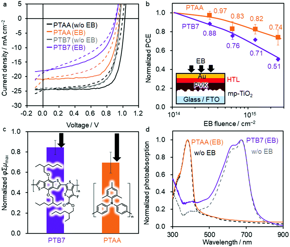 | ||
| Fig. 3 (a) JV curve of the best-performing regular PSC of Device 5 (FTO/cTiO2/mpTiO2/PVK/PTB7/Au) and Device 6 (FTO/cTiO2/mpTiO2/PVK/PTAA/Au) with (purple and orange lines) and without EB exposure (black and grey curves, FEB = 2.5 × 1015 cm−2). The solid and dashed lines are the reverse and forward scans, respectively. (b) Decrease of PCE upon EB irradiation normalized by each initial PCE value. Average values are superimposed. Schematic shows the device structure and EB irradiation geometry. (c) φΣμmax of TRMC transients normalized by the as-prepared PTB7 or PTAA layer (λex = 355 nm, I0 = 2.0 × 10¹⁶ and 1.3 × 10¹⁶ photons cm−2 pulse−1 for PTB7 and PTAA, respectively). The chemical structures are superimposed. The arrows represent the change from the original value without EB irradiation. (d) Normalized photoabsorption spectra of PTB7 and PTAA films before (dotted lines) and after EB exposure (purple and orange lines, FEB = 2.5 × 1015 cm−2). | ||
The effects of radiation exposure on the PTB7 and PTAA layers were studied using TRMC measurements to clarify the difference in the radiation tolerance of these polymers. Results indicate a decrease in φΣμmax after EB irradiation (85 and 70%, respectively), which suggests that a decrease in the charge mobility could be the reason for the reduced JSC (Fig. 3c). The highest occupied molecular orbital (HOMO) levels of PTB7 and PTAA were evaluated using PYS (Fig. S7, ESI†). With increasing EB fluence, the HOMO level of both polymers became deeper from approximately −5.3 to −6.2 eV, which is opposite to the shallowing of the CuSCN VBM. The photoabsorption spectra of the two polymers showed noteworthy differences (Fig. 3d); whereas the peak of PTB7 at 630 nm decreased after EB exposure, almost no change was observed in the spectrum of PTAA. The same change in PTB7 photoabsorption by light irradiation was reported due to the disruption of the π-conjugation.68–70 We assume that EB irradiation induces similar damage to the π-conjugated backbone of PTB7.
Size exclusion chromatography (SEC) measurements were performed to elucidate changes in molecular weights. After EB irradiation at FEB = 2.5 × 1015 cm−2, these polymer films formed an insoluble fraction in chloroform (Fig. S8, ESI†), which was more significant for PTB7 (completely insoluble) than for PTAA (66% soluble fraction). In addition, the molecular weights of both polymers increased with increasing EB fluence (Fig. 4a and b). This suggests that crosslinking reactions occur through the radical coupling of the terminal methyl group of the alkyl side chains.71 Importantly, PTB7 exhibits a rapid overall shift of the SEC profile to a higher molecular weight (Fig. 4a), while PTAA maintains a large part of the original molecular weight distribution (Fig. 4b). This indicates that PTB7 undergoes homogeneous high-density crosslinking, while PTAA undergoes local crosslinking at low density.
 | ||
| Fig. 4 (a) SEC traces (chloroform as the eluent at 40 °C) of (a) PTB7 and (b) PTAA without and with EB exposure. They were evaluated for soluble fractions after EB irradiation. (c) FT-IR spectra (KBr) of PTB7 before and after EB exposure (soluble fraction at FEB = 3.1 × 1014 cm−2). (d) Kinetic analysis of η for PTB7 and PTAA before (black and grey lines) and after EB exposure (purple and orange lines, FEB = 2.5 × 1015 cm−2). | ||
Changes in the chemical structure were evaluated by FT-IR, which revealed a decrease in the peak intensity of the C![[double bond, length as m-dash]](https://www.rsc.org/images/entities/char_e001.gif) O stretching vibration of ester (1730 cm−1) of PTB7 relative to the reference peak intensity at 1460 cm−1 after EB exposure (Fig. 4c and Fig. S9, ESI†). In addition, a change in NMR signals arising from protons of methylene adjacent to oxygen atoms was observed (Fig. S10 and S11, ESI†). The FT-IR and NMR results suggest that the decomposition of side chains via the ester decarboxylation reaction72 occurs in PTB7, which leads to radical-induced crosslinking and the destruction of π-conjugation. Conversely, the FT-IR (Fig. S9b, ESI†) and NMR spectra (Fig. S12 and S13, ESI†) did not change significantly after EB irradiation for PTAA. This indicates that crosslinking, which is assumed to occur through the radical coupling of methyl groups (Fig. S14, ESI†), is limited in PTAA. Thus, the simpler molecular structure of PTAA confers a high radiation tolerance because its main chain comprises many aromatics and is less conjugated.73
O stretching vibration of ester (1730 cm−1) of PTB7 relative to the reference peak intensity at 1460 cm−1 after EB exposure (Fig. 4c and Fig. S9, ESI†). In addition, a change in NMR signals arising from protons of methylene adjacent to oxygen atoms was observed (Fig. S10 and S11, ESI†). The FT-IR and NMR results suggest that the decomposition of side chains via the ester decarboxylation reaction72 occurs in PTB7, which leads to radical-induced crosslinking and the destruction of π-conjugation. Conversely, the FT-IR (Fig. S9b, ESI†) and NMR spectra (Fig. S12 and S13, ESI†) did not change significantly after EB irradiation for PTAA. This indicates that crosslinking, which is assumed to occur through the radical coupling of methyl groups (Fig. S14, ESI†), is limited in PTAA. Thus, the simpler molecular structure of PTAA confers a high radiation tolerance because its main chain comprises many aromatics and is less conjugated.73
The hole-transfer yield (η) from the perovskite to PTB7 and PTAA was evaluated by comparing the TRMC kinetics of mpTiO2/PVK and mpTiO2/PVK/HTM as set out in our previous report.67Fig. 4d shows that holes are efficiently transferred to both HTMs within 10 μs before EB exposure (saturated η, ηsat, reaches 0.95–0.96; see Table S2 and Fig. S15, ESI†). After EB irradiation at FEB = 2.5 × 1015 cm−2, the ηsat of PVK/PTB7 significantly decreases to 0.58, whereas that of PVK/PTAA is maintained at a high value of 0.93 owing to its radiation-tolerant chemical structure.
Fig. 5a summarises the impact of EB exposure on the normalised PCEs for various PSC structures. Whereas the regular PSC using PTAA demonstrates the highest radiation tolerance, the other devices suffer from a large decrease in JSC and fill factor (FF) and a moderate decrease in the open-circuit voltage (VOC) (Fig. S16, ESI†). Despite using TiO2 as an ETM, the regular PSCs comprising CuSCN, Spiro-OMeTAD, or PTB7 as the HTM show similar low radiation tolerance. Inverted PSCs using fullerene derivatives (C60 and PCBM) as the ETM are more susceptible to EB irradiation than regular PSCs possibly due to a high likelihood of polymerisation of the fullerene molecules. The average PCEs before and after EB irradiation at 2.5 × 1015 cm−2 are shown in Fig. 5b. While a comparably high efficiency is maintained for Devices 1 (10.12 ± 1.33%) and 6 (10.86 ± 0.13%), the low-degree of degradation of Device 6 (with PTAA as HTM) is indispensable for prolonged use in space. This is because a large change in the PCE during operation leads to a difficulty of energy dissipation in the initial period without degradation in an isolated space environment.
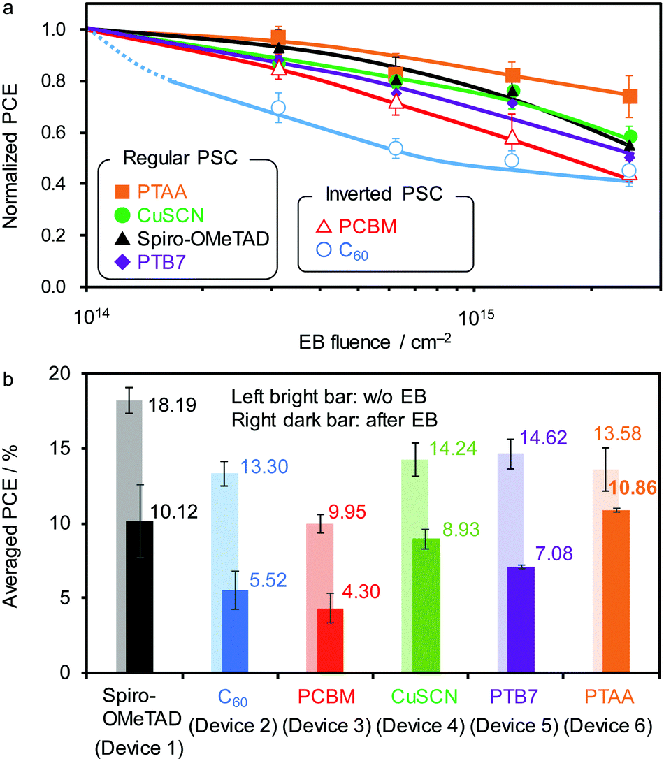 | ||
| Fig. 5 (a) Normalized PCE of various PSCs upon EB exposure. (b) Average PCE values with error bars (standard deviation) before (left bar) and after EB (right bar, FEB = 2.5 × 1015 cm−2) exposure. | ||
Conclusions
We investigated the effect of 100 keV EB exposure on the regular and inverted structures of PSCs with different types of HTMs (Spiro-OMeTAD, CuSCN, PEDOT:PSS, 2PACz, PTB7, and PTAA) and ETMs (TiO2, C60, and PCBM). Inverted PSCs using fullerene derivatives exhibited the lowest radiation tolerance owing to EB-induced polymerisation and degradation of the photoconductivity. Regular PSCs using inorganic CuSCN as the HTM also underwent large degradation upon EB exposure, which was linked to defect formation, as supported by the large decreases in the φΣμmax and τ of TRMC, weakened photoabsorption peak, and shallowing of VBM levels. Of the regular PSCs using TiO2 as the ETM, the device with doped PTAA as the HTM was identified to possess the highest radiation tolerance, maintaining 74% of the initial PCE after FEB = 2.5 × 1015 cm−2 irradiation. This is possibly because of its simple molecular structure, making it less likely to be polymerised or decomposed by radiation than PTB7, which possesses many cleavage and reactive structures. Notably, PTAA exhibited negligible changes in its optical properties and η following EB exposure. Our findings and mechanical insights into radiation-induced degradation are important for developing radiation-tolerant PSCs for applications in space.Experimental
Device fabrication: regular PSCs
A FTO layer on a glass substrate was etched with 6 mol dm−3 HCl and Zn using masking tape. After cleaning with detergent, acetone, isopropyl alcohol, and deionized water, a compact TiO2 (cTiO2) layer was deposited onto the FTO/glass by spray pyrolysis using a solution of titanium diisopropoxide bis(acetylacetonate) (Tokyo Chemical Industry Co. Ltd, TCI) in ethanol (1![[thin space (1/6-em)]](https://www.rsc.org/images/entities/char_2009.gif) :14 v/v) at 450 °C. A 200 nm-thick mesoporous TiO2 (mpTiO2) layer (average particle size: 30 nm, anatase) was deposited onto the compact TiO2 layer by spin-coating (slope 3 s, 5000 rpm for 15 s, slope 2 s) of a diluted TiO2 paste (PST–30NR-D, GreatCell Solar Ltd.) in ethanol (paste:ethanol = 1:7 w/w), followed by sintering at 500 °C for 20 min. A 1.4 M N,N′-dimethylformamide (DMF, super dehydrated, Wako):dimethyl sulfoxide (DMSO, super dehydrated, Wako) = 4:1 (v/v%) solution of FAI ((NH2)2CHI), PbI2, MABr (CH3NH3Br), and PbBr2 with a 0.87:0.13 stoichiometry (the amount of FAI was reduced to FAI/PbI2 = 0.95) was prepared in an N2-filled glovebox. These perovskite precursors of solar cell grade were purchased from Tokyo Chemical Inc. (TCI) and used as received. Subsequently, a precursor layer was formed by spin-coating the solution (slope 1 s, 1000 rpm for 10 s, slope of 4 s, 4500 rpm for 30 s, slope of 2 s). After 35 s, poor-solvent treatment (chlorobenzene, anhydrous 99.8%, Sigma-Aldrich) was applied by slowly dropping 180 μL onto the rotating substrate. The resultant transparent film was annealed at 100 °C for 40 min, resulting in a 300 nm-thick perovskite layer. Each HTLs (Spiro-OMeTAD, CuSCN, PTB7, PTAA) were fabricated on the perovskite layer by the procedure shown below. A 50 nm-thick of Spiro-OMeTAD (Borun New Material Technology Ltd.) was deposited by spin-coating of 78.2 mg mL−1 chlorobenzene (Sigma-Aldrich, anhydrous, 99.8%) with 52 mol% of LiTFSI (TCI, TFSI is bis(trifluoro methanesulfonyl)imide) and 5.4 mol% Co(TFSI)2 (FK209, Lumtec Inc.) relative to SpiroOMeTAD dissolved in acetonitrile (Sigma-Aldrich, anhydrous, 99.8%) and 2.9 vol% 4-tert-butylpyridine (TBP, Sigma-Aldrich, 98%) relative to the solution volume. A 50 nm-thick of CuSCN (Aldrich) was deposited by spin-coating of 35 mg mL−1 diethyl sulfide (TCI, 98%). A 25 nm-thick of PTB7 (1-Materials Inc.) was deposited by spin-coating of 10 mg mL−1 chlorobenzene (Sigma-Aldrich, anhydrous, 99.8%). A 25 nm-thick of PTAA (Aldrich) was deposited by spin-coating of 10 mg mL−1 toluene (Wako, anhydrous, 99.5%) with 0.15 vol% of LiTFSI solution (100 mg mL−1 TBP). Subsequently, a 70 nm-thick stripe-shaped gold electrode was thermally deposited in a vacuum chamber. To promote oxygen doping of HTM, devices were stored in an oxygen-substituted desiccator in the dark for 3 days. Current–voltage curves were measured using a source-meter unit (ADCMT Corp., 6241A) under AM1.5G solar illumination at 100 mW cm−2 (1 sun, monitored by a calibrated standard cell, Bunko Keiki BS-520BK) from a 300 W solar simulator (SAN-EI Corp., XES-301S). The size of the active area was defined by a black metal mask with a square hole (2 × 2 mm2). The monochromated light power was calibrated using a silicon photovoltaic cell (Bunko Keiki model S1337-1010BQ).
:14 v/v) at 450 °C. A 200 nm-thick mesoporous TiO2 (mpTiO2) layer (average particle size: 30 nm, anatase) was deposited onto the compact TiO2 layer by spin-coating (slope 3 s, 5000 rpm for 15 s, slope 2 s) of a diluted TiO2 paste (PST–30NR-D, GreatCell Solar Ltd.) in ethanol (paste:ethanol = 1:7 w/w), followed by sintering at 500 °C for 20 min. A 1.4 M N,N′-dimethylformamide (DMF, super dehydrated, Wako):dimethyl sulfoxide (DMSO, super dehydrated, Wako) = 4:1 (v/v%) solution of FAI ((NH2)2CHI), PbI2, MABr (CH3NH3Br), and PbBr2 with a 0.87:0.13 stoichiometry (the amount of FAI was reduced to FAI/PbI2 = 0.95) was prepared in an N2-filled glovebox. These perovskite precursors of solar cell grade were purchased from Tokyo Chemical Inc. (TCI) and used as received. Subsequently, a precursor layer was formed by spin-coating the solution (slope 1 s, 1000 rpm for 10 s, slope of 4 s, 4500 rpm for 30 s, slope of 2 s). After 35 s, poor-solvent treatment (chlorobenzene, anhydrous 99.8%, Sigma-Aldrich) was applied by slowly dropping 180 μL onto the rotating substrate. The resultant transparent film was annealed at 100 °C for 40 min, resulting in a 300 nm-thick perovskite layer. Each HTLs (Spiro-OMeTAD, CuSCN, PTB7, PTAA) were fabricated on the perovskite layer by the procedure shown below. A 50 nm-thick of Spiro-OMeTAD (Borun New Material Technology Ltd.) was deposited by spin-coating of 78.2 mg mL−1 chlorobenzene (Sigma-Aldrich, anhydrous, 99.8%) with 52 mol% of LiTFSI (TCI, TFSI is bis(trifluoro methanesulfonyl)imide) and 5.4 mol% Co(TFSI)2 (FK209, Lumtec Inc.) relative to SpiroOMeTAD dissolved in acetonitrile (Sigma-Aldrich, anhydrous, 99.8%) and 2.9 vol% 4-tert-butylpyridine (TBP, Sigma-Aldrich, 98%) relative to the solution volume. A 50 nm-thick of CuSCN (Aldrich) was deposited by spin-coating of 35 mg mL−1 diethyl sulfide (TCI, 98%). A 25 nm-thick of PTB7 (1-Materials Inc.) was deposited by spin-coating of 10 mg mL−1 chlorobenzene (Sigma-Aldrich, anhydrous, 99.8%). A 25 nm-thick of PTAA (Aldrich) was deposited by spin-coating of 10 mg mL−1 toluene (Wako, anhydrous, 99.5%) with 0.15 vol% of LiTFSI solution (100 mg mL−1 TBP). Subsequently, a 70 nm-thick stripe-shaped gold electrode was thermally deposited in a vacuum chamber. To promote oxygen doping of HTM, devices were stored in an oxygen-substituted desiccator in the dark for 3 days. Current–voltage curves were measured using a source-meter unit (ADCMT Corp., 6241A) under AM1.5G solar illumination at 100 mW cm−2 (1 sun, monitored by a calibrated standard cell, Bunko Keiki BS-520BK) from a 300 W solar simulator (SAN-EI Corp., XES-301S). The size of the active area was defined by a black metal mask with a square hole (2 × 2 mm2). The monochromated light power was calibrated using a silicon photovoltaic cell (Bunko Keiki model S1337-1010BQ).
Device fabrication: inverted PSCs
An indium tin oxide (ITO) layer on a glass substrate was etched and cleaned above procedure. Self-assembled monolayer of 2PACz (TCI) dissolved in ethanol (Wako, anhydrous, 99.5%) was deposited by spin-coating followed by thermal annealing at 100 °C for 10 min. A PEDOT:PSS layer (Clevios P VP AI 4083, 50 nm) was deposited on ITO glass by spin-coating at 4000 rpm for 60 s followed by thermal annealing at 140 °C for 20 min. Perovskite layer was fabricated by the same procedure as regular PSCs. Each ETL (C60 or PCBM) and buffer layer (bathocuproine: BCP or N,N′-Bis(N,N-dimethylpropan-1-amine oxide) perylene-3,4,9,10-tetracarboxylic diimide: PDINO) were fabricated by the procedure shown below. A 50 nm-thick C60 (Frontier Carbon Inc.) and 8 nm-thick BCP (TCI) were thermally deposited in a vacuum chamber. A 25 nm-thick PCBM (Frontier Carbon Inc.) dissolved in 20 mg mL−1 chlorobenzene (Sigma-Aldrich, anhydrous, 99.8%) and PDINO (Ossila) dissolved in 1 mg mL−1 methanol (Wako, anhydrous, 99.5%) were deposited by spin-coating (15 nm). Finally, a 100 nm-thick stripe-shaped silver electrode was thermally deposited in a vacuum chamber.EB exposure
An electron beam (100 keV) was exposed from the layer side (not from the glass side) in a vacuum chamber (50 Pa) using a Hamamatsu Photonics EB-ENGINE system.Time-resolved microwave conductivity (TRMC)
Perovskite, mpTiO2, HTM, and their composite layers were prepared in the same manner as the solar cells on a quartz plate. The sample was set in a resonant cavity and probed by continuous microwaves at ca. 9.1 GHz. The excitation laser from an optical parametric oscillator (OPO, Continuum Inc., Panther) seeded by the third harmonic generation (355 nm) of a Nd:YAG laser (Continuum Inc., Surelite II, 5–8 ns pulse duration, 10 Hz) was set to 500 nm at I0 = 1.3 × 10¹¹ photons cm−2 pulse−1 or 355 nm at I0 = 7.0 × 10¹⁵, 1.3 × 10¹⁶, or 2.0 × 10¹⁶ photons cm−2 pulse−1. The laser pulse was exposed from the top side (not from the quartz side). The photoconductivity transient Δσ was converted to the product of the quantum efficiency (φ) and the sum of the charge carrier mobilities, Σμ (=μh + μe) by φΣμ = Δσ (eI0Flight)−1, where e and FLight are the unit charge of a single electron and a correction (or filling) factor, respectively. All experiments were conducted at 25 °C in air.General measurement
Steady-state photoabsorption spectroscopy was performed using a Jasco V-730 ultraviolet-visible (UV-Vis) spectrophotometer. Fourier transform infrared (FT-IR) spectroscopy was performed using a Jasco FT/IR-4700AC spectrometer. Photoelectron yield spectroscopy (PYS) measurements were performed using Bunko Keiki BIP-KV202GD. X-ray diffraction (XRD) measurements were performed using a Rigaku Corp. MiniFlex-600 instrument (CuKα radiation: λ = 1.54 Å). XPS measurements were conducted using a JEOL JPS-9010MC. The thickness of a layer was measured using a Bruker Dektak XT surface profiler. Size exclusion chromatography (SEC) analysis with polystyrene standards was performed with chloroform as an eluent at a flow rate of 1 cm3 min−1 at 40 °C, on a Shimadzu LC-20AT, CBM-20A, CTO-20A chromatography instrument connected to a Shimadzu SPD-M20A UV-vis detector. 1H NMR (400 MHz) charts were measured on a JEOL JNM-ECZS400 spectrometer at room temperature.Author contributions
Y. M. performed the experiments, analysed the data, and wrote the manuscript. R. N. and F. I. supported the experiments, analyses, and discussion. K. O. and T. K. provided the EB exposure facility and supported the experiments. A. S. conceived and designed the research, analysed the data, and wrote the manuscript. All the authors read the manuscript, discussed the content, and made feedback.Conflicts of interest
The authors declare no competing financial interests.Acknowledgements
We acknowledge financial support from Core Research for Evolutional Science and Technology (CREST) (Grant No. JPMJCR2107), and the MIRAI program (Grant No. JPMJMI22E2) of the Japan Science and Technology Agency (JST); Green Innovation Program (Grant No. JP21578854) of the New Energy and Industrial Technology Development Organization (NEDO); and KAKENHI from the Japan Society for the Promotion of Science (JSPS) (Grant No. JP20H05836 and JP20H00398).Notes and references
- F. Dimroth, Phys. Status Solidi C, 2006, 3, 373–379 CrossRef CAS.
- M. Bosi and C. Pelosi, Prog. Photovoltaics, 2007, 15, 51–68 CAS.
- M. Imaizumi, T. Nakamura, T. Takamoto, T. Ohshima and M. Tajima, Prog. Photovoltaics, 2017, 25, 161–174 CAS.
- C. Morioka, K. Shimazaki, S. Kawakita, M. Imaizumi, H. Yamaguchi, T. Takamoto, S.-i Sato, T. Ohshima, Y. Nakamura, K. Hirako and M. Takahashi, Prog. Photovoltaics, 2011, 19, 825–833 CAS.
- D. Maurin, F. Melot and R. Taillet, Astron. Astrophys., 2014, 569, A32 CrossRef.
- B. Pasquale, Astron. Astrophys. Rev., 2013, 21, 70 CrossRef.
- A. Hamache, N. Sengouga, A. Meftah and M. Henini, Radiat. Phys. Chem., 2016, 123, 103–108 CrossRef CAS.
- A. M. Saad, Can. J. Phys., 2002, 80, 1591–1599 CrossRef CAS.
- T. Aburaya, T. Hisamatsu and S. Matsuda, Sol. Energy Mater. Sol. Cells, 2001, 68, 15–22 CrossRef CAS.
- A. Kojima, K. Teshima, Y. Shirai and T. Miyasaka, J. Am. Chem. Soc., 2009, 131, 6050–6051 CrossRef CAS.
- H.-S. Kim, C.-R. Lee, J.-H. Im, K.-B. Lee, T. Moehl, A. Marchioro, J. S. Moon, R. Humphry-Baker, J.-H. Yum, J. E. Moser, M. Grätzel and N.-G. Park, Sci. Rep., 2012, 2, 591 CrossRef PubMed.
- M. M. Lee, J. Teuscher, T. Miyasaka, T. N. Murakami and H. J. Snaith, Science, 2012, 338, 643–647 CrossRef CAS PubMed.
- H. Oga, A. Saeki, Y. Ogomi, S. Hayase and S. Seki, J. Am. Chem. Soc., 2014, 136, 13818–13825 CrossRef CAS PubMed.
- H. Zhang, E. Debroye, J. A. Steele, M. B.-J. Roeffaers, J. Hofkens, H. I. Wang and M. Bonn, ACS Energy Lett., 2021, 6, 568–573 CrossRef CAS.
- L. M. Pazos-Outón, M. Szumilo, R. Lamboll, J. M. Richter, M. Crespo-Quesada, M. Abdi-Jalebi, H. J. Beeson, M. Vrućinić, M. Alsari, H. J. Snaith, B. Ehrler, R. H. Friend and F. Deschler, Science, 2016, 351, 1430–1433 CrossRef PubMed.
- N. Wang, L. Cheng, R. Ge, S. Zhang, Y. Miao, W. Zou, C. Yi, Y. Sun, Y. Cao, R. Yang, Y. Wei, Q. Guo, Y. Ke, M. Yu, Y. Jin, Y. Liu, Q. Ding, D. Di, L. Yang, G. Xing, H. Tian, C. Jin, F. Gao, R. H. Friend, J. Wang and W. Huang, Nat. Photonics, 2016, 10, 699–704 CrossRef CAS.
- L. Shen, Y. Fang, D. Wang, Y. Bai, Y. Deng, M. Wang, Y. Lu and J. Huang, Adv. Mater., 2016, 28, 10794–10800 CrossRef CAS PubMed.
- A. Walsh, D. O. Scanlon, S. Chen, X. Gong and S.-H. Wei, Angew. Chem., Int. Ed., 2015, 54, 1791–1794 CrossRef CAS PubMed.
- R. E. Brandt, J. R. Poindexter, P. Gorai, R. C. Kurchin, R. L.-Z. Hoye, L. Nienhaus, M. W.-B. Wilson, J. A. Polizzotti, R. Sereika, R. Žaltauskas, L. C. Lee, J. L. MacManus-Driscoll, M. Bawendi, V. Stevanović and T. Buonassisi, Chem. Mater., 2017, 29, 4667–4674 CrossRef CAS.
- W. J. Yin, J. H. Yang, J. Kang, Y. Yan and S. H. Wei, J. Mater. Chem. A, 2015, 3, 8926–8942 RSC.
- H. Min, D. Y. Lee, J. Kim, G. Kim, K. S. Lee, J. Kim, M. J. Paik, Y. K. Kim, K. S. Kim, M. G. Kim, T. J. Shin and S. Il Seok, Nature, 2021, 598, 444–450 CrossRef CAS PubMed.
- L. K. Reb, M. Böhmer, B. Predeschly, S. Grott, C. L. Weindl, G. I. Ivandekic, R. Guo, C. Dreißigacker, R. Gernhäuser, A. Meyer and P. Müller-Buschbaum, Joule, 2020, 4, 1880–1892 CrossRef CAS.
- W. Chen, X. Li, Y. Li and Y. Li, Energy Environ. Sci., 2020, 13, 1971–1996 RSC.
- J. Y. Kim, J.-W. Lee, H. S. Jung, H. Shin and N.-G. Park, Chem. Rev., 2020, 120, 7867–7918 CrossRef CAS PubMed.
- A. K. Jena, A. Kulkarni and T. Miyasaka, Chem. Rev., 2019, 119, 3036–3103 CrossRef CAS PubMed.
- L. Mao, C. C. Stoumpos and M. G. Kanatzidis, J. Am. Chem. Soc., 2019, 141, 1171–1190 CrossRef CAS PubMed.
- J. S. Manser, J. A. Christians and P. V. Kamat, Chem. Rev., 2016, 116, 12956–13008 CrossRef CAS.
- W. Zhang, G. E. Eperon and H. J. Snaith, Nat. Energy, 2016, 1, 16048 CrossRef CAS.
- P. Gao, M. Grätzel and M. K. Nazeeruddin, Energy Environ. Sci., 2014, 7, 2448–2463 RSC.
- Y. Miyazawa, M. Ikegami, H.-W. Chen, T. Ohshima, M. Imaizumi, K. Hirose and T. Miyasaka, iScience, 2018, 2, 148–155 CrossRef CAS PubMed.
- C. D. Bailie, M. G. Christoforo, J. P. Mailoa, A. R. Bowring, E. L. Unger, W. H. Nguyen, J. Burschka, N. Pellet, J. Z. Lee, M. Grätzel, R. Noufi, T. Buonassisi, A. Salleo and M. D. McGehee, Energy Environ. Sci., 2015, 8, 956–963 RSC.
- F. Fu, T. Feurer, T. Jäger, E. Avancini, B. Bissig, S. Yoon, S. Buecheler and A. N. Tiwari, Nat. Commun., 2015, 6, 8932 CrossRef CAS PubMed.
- F. Lang, M. Jošt, K. Frohna, E. Köhnen, A. Al-Ashouri, A. R. Bowman, T. Bertram, A. B. Morales-Vilches, D. Koushik, E. M. Tennyson, K. Galkowski, G. Landi, M. Creatore, B. Stannowski, C. A. Kaufmann, J. Bundesmann, J. Rappich, B. Rech, A. Denker, S. Albrecht, H. C. Neitzert, N. H. Nickel and S. D. Stranks, Joule, 2020, 4, 1054–1069 CrossRef CAS PubMed.
- G. E. Eperon, T. Leijtens, K. A. Bush, R. Prasanna, T. Green, J. T.-W. Wang, D. P. McMeekin, G. Volonakis, R. L. Milot, R. May, A. Palmstrom, D. J. Slotcavage, R. A. Belisle, J. B. Patel, E. S. Parrott, R. J. Sutton, W. Ma, F. Moghadam, B. Conings, A. Babayigit, H.-G. Boyen, S. Bent, F. Giustino, L. M. Herz, M. B. Johnston, M. D. McGehee and H. J. Snaith, Science, 2016, 354, 861–865 CrossRef CAS PubMed.
- R. Lin, K. Xiao, Z. Qin, Q. Han, C. Zhang, M. Wei, M. I. Saidaminov, Y. Gao, J. Xu, M. Xiao, A. Li, J. Zhu, E. H. Sargent and H. Tan, Nat. Energy, 2019, 4, 864–873 CrossRef CAS.
- F. Lang, G. E. Eperon, K. Frohna, E. M. Tennyson, A. Al-Ashouri, G. Kourkafas, J. Bundesmann, A. Denker, K. G. West, L. C. Hirst, H. C. Neitzert and S. D. Stranks, Adv. Energy Mater., 2021, 11, 2102246 CrossRef CAS.
- D. P. McMeekin, G. Sadoughi, W. Rehman, G. E. Eperon, M. Saliba, M. T. Hörantner, A. Haghighirad, N. Sakai, L. Korte, B. Rech, M. B. Johnston, L. M. Herz and H. J. Snaith, Science, 2016, 351, 151–155 CrossRef CAS PubMed.
- B. Chen, Y. Bai, Z. Yu, T. Li, X. Zheng, Q. Dong, L. Shen, M. Boccard, A. Gruverman, Z. Holman and J. Huang, Adv. Energy Mater., 2016, 6, 1601128 CrossRef.
- W. Guter, F. Dunzer, L. Ebel, K. Hillerich, W. Köstler, T. Kubera, M. Meusel, B. Postels and C. Wächter, E3S Web Conf., 2017, 16, 03005 CrossRef.
- W. O.-H. Martínez, N. B.-C. Guerrero, V. A. G. Andrade, M. Alurralde and M. D. Perez, Sol. Energy Mater. Sol. Cells, 2022, 238, 111644 CrossRef.
- Y. Murakami, F. Ishiwari, K. Okamoto, T. Kozawa and A. Saeki, ACS Appl. Mater. Interfaces, 2021, 13, 24824–24832 CrossRef CAS PubMed.
- Y. Wang, Z. Gu, Y. Ren, Z. Wang, B. Yao, Z. Dong, G. Adamo, H. Zeng and H. Sun, ACS Appl. Mater. Interfaces, 2019, 11, 15756–15763 CrossRef CAS PubMed.
- M. Palei, M. Motapothula, A. Ray, A. L. Abdelhady, L. Lanzano, M. Prato, J. K. Panda, A. Scarpellini, V. Pellegrini, D. Primetzhofer, U. Petralanda, L. Manna and Z. Dang, J. Mater. Chem. C, 2020, 8, 9923–9930 RSC.
- G. M. Paternò, V. Robbiano, L. Santarelli, A. Zampetti, C. Cazzaniga, G. V. Sakai and F. Cacialli, Sustainable Energy Fuels, 2019, 3, 2561–2566 RSC.
- S. Yang, Z. Xu, S. Xue, P. Kandlakunta, L. Cao and J. Huang, Adv. Mater., 2019, 31, 1805547 CrossRef PubMed.
- K. Yang, K. Huang, X. Li, S. Zheng, P. Hou, J. Wang, H. Guo, H. Song, B. Li, H. Li, B. Liu, X. Zhong and J. Yang, Org. Electron., 2019, 71, 79–84 CrossRef CAS.
- N. Klein-Kedem, D. Cahen and G. Hodes, Acc. Chem. Res., 2016, 49, 347–354 CrossRef CAS PubMed.
- P. Li, H. Dong, J. Lan, Y. Bai, C. He, L. Ma, Y. Li and J. Liu, Materials, 2022, 15, 1393 CrossRef CAS PubMed.
- A. Saeki, Polym. J., 2020, 52, 1307–1321 CrossRef CAS PubMed.
- N. R. Venkatesan, J. G. Labram and M. L. Chabinyc, ACS Energy Lett., 2018, 3, 380–386 CrossRef CAS.
- E. M. Hutter, M. C. Gélvez-Rueda, A. Osherov, V. Bulovic, F. C. Grozema, S. D. Stranks and T. J. Savenije, Nat. Mater., 2017, 16, 115–120 CrossRef CAS PubMed.
- M. Ferry, Y. Ngono-Ravache, V. Picq and E. Balanzat, J. Phys. Chem. B, 2008, 112, 10879–10889 CrossRef CAS PubMed.
- National Research Council, Health Risks from Exposure to Low Levels of Ionizing Radiation: BEIR VII Phase 2, The National Academies Press, Washington, DC, 2006, DOI:10.17226/11340.
- Y. M. Seo, Y. H. Kim, S. H. Park and J. Seon, Curr. Appl. Phys., 2012, 12, 1541–1547 CrossRef.
- N. Wang, K. Zhao, T. Ding, W. Liu, A. S. Ahmed, Z. Wang, M. Tian, X. W. Sun and Q. Zhang, Adv. Energy Mater., 2017, 7, 1700522 CrossRef.
- A. A. Said, J. Xie and Q. Zhang, Small, 2019, 15, 1900854 CrossRef PubMed.
- A. Al-Ashouri, A. Magomedov, M. Roß, M. Jošt, M. Talaikis, G. Chistiakova, T. Bertram, J. A. Márquez, E. Köhnen, E. Kasparavičius, S. Levcenco, L. Gil-Escrig, C. J. Hages, R. Schlatmann, B. Rech, T. Malinauskas, T. Unold, C. A. Kaufmann, L. Korte, G. Niaura, V. Getautis and S. Albrecht, Energy Environ. Sci., 2019, 12, 3356–3369 RSC.
- J. Min, Z. G. Zhang, Y. Hou, C. O.-R. Quiroz, T. Przybilla, C. Bronnbauer, F. Guo, K. Forberich, H. Azimi, T. Ameri, E. Spiecker, Y. Li and C. J. Brabec, Chem. Mater., 2015, 27, 227–234 CrossRef CAS.
- Y. Maeyoshi, A. Saeki, S. Suwa, M. Omichi, H. Marui, A. Asano, S. Tsukuda, M. Sugimoto, A. Kishimura, K. Kataoka and S. Seki, Sci. Rep., 2012, 2, 600 CrossRef PubMed.
- N. Wijeyasinghe and T. D. Anthopoulos, Semicond. Sci. Technol., 2015, 30, 104002 CrossRef.
- N. Arora, M. I. Dar, A. Hinderhofer, N. Pellet, F. Schreiber, S. M. Zakeeruddin and M. Grätzel, Science, 2017, 358, 768–771 CrossRef CAS PubMed.
- P. Pattanasattayavong, D. M. Packwood and D. J. Harding, J. Mater. Chem. C, 2019, 7, 12907–12917 RSC.
- M. J. Patel, S. K. Gupta and P. N. Gajjar, Mater. Today: Proc., 2020, 28, 164–167 CAS.
- W. Ji, G. Q. Yue, F. S. Ke, S. Wu, H. B. Zhao, L. Y. Chen, S. Y. Wang and Y. Jia, J. Korean Phys. Soc., 2012, 60, 1253–1257 CrossRef CAS.
- Y. Du, H. Cai, J. Ni, J. Li, H. Yu, X. Sun, Y. Wu, H. Wen and J. Zhang, RSC Adv., 2015, 5, 66981–66987 RSC.
- F. M. Rombach, S. A. Haque and T. J. Macdonald, Energy Environ. Sci., 2021, 14, 5161–5190 RSC.
- N. Ishida, A. Wakamiya and A. Saeki, ACS Photonics, 2016, 3, 1678–1688 CrossRef CAS.
- S. Kim, M. A.-M. Rashid, T. Ko, K. Ahn, Y. Shin, S. Nah, M. H. Kim, B. S. Kim, K. Kwak and M. Cho, J. Phys. Chem. C, 2020, 124, 2762–2770 CrossRef CAS.
- J. Razzell-Hollis, J. Wade, W. C. Tsoi, Y. Soon, J. Durrant and J. S. Kim, J. Mater. Chem. A, 2014, 2, 20189–20195 RSC.
- S. Alem, S. Wakim, J. Lu, G. Robertson, J. Ding and Y. Tao, ACS Appl. Mater. Interfaces, 2012, 4, 2993–2998 CrossRef CAS PubMed.
- M. Bednarek, K. Borska and P. Kubisa, Molecules, 2020, 25, 4919–4947 CrossRef CAS PubMed.
- V. N. Belevskii and S. I. Belopushkin, High Energy Chem., 2005, 39, 69–76 CrossRef CAS.
- O. A. Aldaghri, B. A. El-Badry, M. K.-M. Ali and K. H. Ibnaouf, Appl. Sci., 2022, 12, 1606–1615 CrossRef CAS.
Footnote |
| † Electronic supplementary information (ESI) available. See DOI: https://doi.org/10.1039/d2ma00385f |
| This journal is © The Royal Society of Chemistry 2022 |