
 Open Access Article
 This Open Access Article is licensed under a Creative Commons Attribution-Non Commercial 3.0 Unported Licence
An efficient dual functional Raman and Fluorescence detection platform achieved by controlling the electromagnetic enhanced field in three-dimensional Ag/ZnO composited arrays†
Yongqi
Yin
 *ab,
Xiao
Liu
bc,
Mengqi
Wang
a,
Shuang
Li
a,
Yan
Chen
a and
Ye
Sun
*d
*ab,
Xiao
Liu
bc,
Mengqi
Wang
a,
Shuang
Li
a,
Yan
Chen
a and
Ye
Sun
*d
aKey Laboratory for Photonic and Electronic Bandgap Materials, Ministry of Education, School of Physics and Electronic Engineering, Harbin Normal University, Harbin, 150025, China. E-mail: echo.929@163.com
bCondensed Matter Science and Technology Institute, Harbin Institute of Technology, Harbin, China
cSpecial Division of Environmental and Energy Science, Komaba Organization for Educational Excellence (KOMEX), College of Arts and Sciences, University of Tokyo, Tokyo 153-8902, Japan
dSchool of Instrumentation Science and Engineering, Harbin Institute of Technology, Harbin 150080, China. E-mail: sunye@hit.edu.cn
First published on 29th April 2022
Abstract
Surface-enhanced Raman scattering (SERS) and metal-enhanced fluorescence (MEF) phenomena can significantly increase spectroscopic signals, allowing sophisticated biological detection to be realized. However, integrating SERS and MEF into a single plasmonic platform is still a challenge, since the optimized distance between the analyte and the metal is different for these two detection techniques. Herein, we designed a three-dimensional (3D) electromagnetic field via decorating silver (Ag) nanoparticles on a zinc oxide (ZnO) nanorod arrays to overcome this limitation, and the ultrasensitive detection of Rhodamine 6G dye molecules at extremely low detection limits of 10 fM for SERS and 100 fM for MEF can be realized. The underlying enhancement mechanism investigated via finite-difference time-domain simulations revealed that the 3D electromagnetic field could overcome the quenching effect in MEF to achieve the simultaneous enhancement of the SERS and MEF signals. This work provides a way to apply 3D architecture to realize ultrasensitive SERS-MEF dual-mode detection.
Introduction
Surface plasmon-enhanced spectroscopic sensors are highly sensitive and specific analysis tools for bioimaging,1 biosensing,2 clinical diagnostics,3 and environmental monitoring.4 Plasmon nanostructures such as golden (Au) or silver (Ag) nanoparticles (NPs) play a significant role in surface-enhanced techniques.5–9 When the incident light is close to their plasmon resonance, the localized electromagnetic fields are greatly enhanced near the metallic surface, giving rise to phenomena such as surface-enhanced Raman scattering (SERS) and metal/surface-enhanced fluorescence (MEF or SEF).10,11The MEF phenomenon stems from the increased excitation or radiative emission rate of the fluorophore as a result of the interaction between the fluorophore dipole moment and the surface plasmon field of the metallic nanoparticle.10,11 However, the fluorescence signal is typically transferred to fluorescence imaging, and cannot provide structural information of the emitting molecules. On the contrary, SERS measurement can achieve high-level target recognition and offers intrinsic structural information on the analyst with sharp vibrational bands.12 Consequently, it would be desirable to operate a SERS-MEF dual-mode sensing chip to realize the simultaneous detection of an image and structural information of detected molecules in future spectroscopic techniques.
However, it is still challenging to integrate both SERS and MEF in a single platform since the optimum distance from analyte to metal in SERS and MEF is different. The MEF effect relies on a relatively large analyte (fluorophore) to metal distance. A typical distance between the fluorophore and metal should be at least 5–10 nm to overcome the quenching effect from the metal surface. Therefore, dielectric layers or molecules were usually needed to separate the fluorophore from the metallic nanoparticles in previous reports.13 However, an efficient SERS effect requires direct contact of the analyte with the metal since the EM field is localized in spatially narrow regions, such as interparticle nanogaps or particle–substrate nanogaps, known as “hotspots”.
To explore dual-functional SERS and MEF platforms, a variety of geometries of functional nanostructures, such as needle tip or shape edges, aggregated metallic nanoparticles and metallic/dielectric core/shell composited nanostructures, have been investigated to overcome the challenge of the different optimal distances in the two detection techniques.14–21 However, most sensor systems have applied two-dimensional planar geometries or metallic colloids with a small proportion of hotspot area and limited enhancement factors. Thus, a rationally designed nanostructure with large-area hotspots in three dimensions (3D) might achieve an optimal enhancement toward performing dual-functional SERS-MEF analysis.
Herein, we investigated a plasmonic nanohybrid combining Ag nanoparticles and ZnO NR arrays to form a three-dimensional (3D) configuration based on our previous works.22,23 The nano-aggregated Ag NPs with a controllable interparticle gap became the plasmonic hotspots for target molecule detection. The c-axis oriented ZnO NR arrays with a large specific surface area would serve as scaffolds to attach the Ag NPs and the target fluorophores. By controlling the size and distribution of Ag NPs on the ZnO nanorod arrays, ultrasensitive SERS and MEF performance with detection limits of 10 fM for SERS and 100 fM for MEF can be realized based on this platform to detect Rhodamine 6G (R6G) molecules. The enhancement mechanism demonstrated by finite-difference time-domain (FDTD) simulations showed a robust spatial distribution of local enhanced electrical fields to overcome the quenching effect in MEF under a certain degree of Ag NP size and distribution, realizing a simultaneous enhancement of the SERS and MEF signals.
Results and discussion
Nanostructure characterization
The 3D Ag/ZnO NR platform can be realized by the deposition of Ag NPs on pre-assembled ZnO NR arrays. The inter-particle nanogaps, size, and distribution of the Ag NPs can be controlled by regulating the fabrication parameters. According to our previous works, ZnO NR arrays were prepared by a facile hydrothermal method (details can be found in the Experimental section).22 The SEM images of the as-prepared ZnO (Fig. S1(a), ESI†) showed that the ZnO NRs were perpendicular to the substrate with a highly ordered hexagonal crystal structure. The average diameter and length were ∼70 nm and ∼670 nm, respectively. Subsequently, the Ag NPs were deposited on the top and surface of the ZnO NRs by a radio frequency magnetron sputtering method. The particle size and the interparticle distance can be controlled by adjusting the sputtering time to 1 min, 5 min, 20 min, and 30 min, respectively (Fig. 1 and Fig. S1, ESI†). The size range of the Ag grains on the top and body of the NRs was estimated as 5–20 nm for 1 min deposition time (Fig. 1a) and 20–50 nm for 5 min (Fig. 1d). With further increasing the deposition time to 20 and 30 min, the size of the Ag NPs was further increased, and the inter-particle spacing was reduced. For 30 min deposited Ag/ZnO NRs, the Ag nanoparticles were too big to merge (Fig. S1, ESI†). The Ag element content in the Ag/ZnO NRs is linearly increased with increasing the deposition time, demonstrated in the energy dispersive spectroscopy (EDS) results in Fig. S1d (ESI†). For the Ag/ZnO NRs, the X-ray diffraction (XRD) pattern (Fig. S2, ESI†) with a dominant (002) crystal face of the ZnO NRs indicates the c-axis preferred growth of the NR arrays. Moreover, the diffraction peaks located at 38.3° and 44.3° can be attributed to the (111) and (200) crystal planes of Ag (JCPDS No. 01-1167). TEM images have further confirmed the size and distribution of Ag NPs. As shown in Fig. 1b, the 1 min-deposited Ag was spherical particles with a size range of 12 ± 3 nm, and the average gap between each Ag NP is over 10 nm. When the deposition time was increased to 5 min, the size of the Ag grains was increased to 25 ± 7 nm (Fig. 1e). The density of Ag NPs was also increased, and this led to the interparticle gap between the Ag NPs being decreased to 2–6 nm. The HRTEM images in Fig. 1c and f show the 1 min and 5 min Ag/ZnO NRs, and the measured spacings of the lattice planes of 0.26 nm and 0.24 nm were related to the (002) and (101) planes of ZnO, and those of 0.24 nm and 0.20 nm were related to the (111) and (200) planes of the Ag crystal lattice.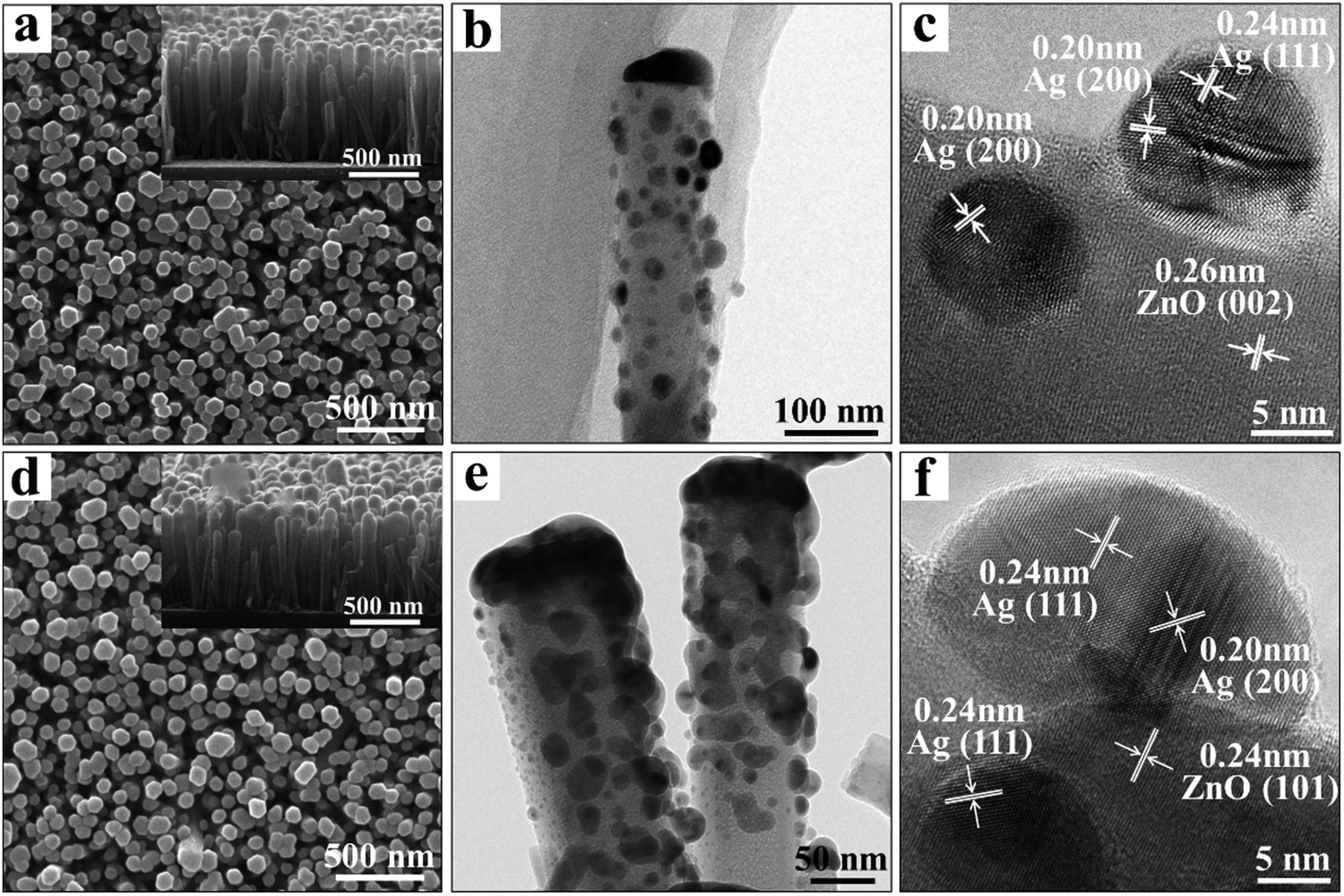 | ||
| Fig. 1 SEM images of Ag/ZnO NRs with Ag-deposition durations of (a) 1 min and (d) 5 min; the inset images show cross-sections. TEM images of Ag/ZnO NRs with Ag-deposition durations of (b) 1 min and (e) 5 min. HRTEM images of Ag/ZnO NRs with Ag-deposition times of (c) 1 min and (f) 5 min. | ||
SERS and MEF characterization
The SERS performances of our Ag/ZnO NR arrays were evaluated under an excitation wavelength of 532 nm. The typical R6G fluorophore, which can be excited at a similar wavelength to the Ag surface plasmon resonance, was selected as the target molecule. The excitation and emission rates of this fluorophore would be enhanced by Ag surface plasmon resonance. A series of as-prepared samples with different Ag sputtering times were immersed in a relatively low concentration of 10−6 M R6G dye for 12 hours at 4 °C, and then washed and dried in air. As illustrated in Fig. 2a, the Raman spectrum shows feature peaks of R6G at 614 cm−1, 773 cm−1, 931 cm−1, 1087 cm−1, 1183 cm−1, 1271 cm−1, 1310 cm−1, 1363 cm−1, 1419 cm−1, 1509 cm−1, 1572 cm−1 and 1650 cm−1, which agreed well with the literature values.24 The chosen specific intensity ratio (the intensity for a certain peak/the background intensity) of 1650 cm−1 and 773 cm−1 (Fig. 2c) showed a trend of increasing enhancement ability with increasing Ag deposition time to 20 min and a little decrease when extending the Ag deposition time to 30 min. The decreased SERS signal in 30 min Ag/ZnO might be due to the aggregation of the Ag NPs (Fig. S1, ESI†), resulting in a reduced effective activity surface and reduced hotspots generated in the gaps of the Ag NPs. The SERS enhancement factor (EF) used to evaluate the Raman enhancement ability of the substrates was further calculated according to the Raman spectra of bare ZnO (reference) and 20 min Ag/ZnO via the formula EF = (ISERS/IREF) × (CREF/CSERS).25,26 Details can be found in the, Fig. S3a (ESI†), and the value of EF was estimated to be 8 × 10¹¹ for our 20 min Ag/ZnO platform, which is higher than the previous report with an average EF of 107–1010.26,27 The detection limit of the R6G molecule was further evaluated with the optimized 20 min-Ag/ZnO NR samples and shown in Fig. S3b (ESI†). Even at a very low concentration of 1 fM, the feature characteristics of the dye molecule can still be observed, verifying the highly sensitive SERS detection ability.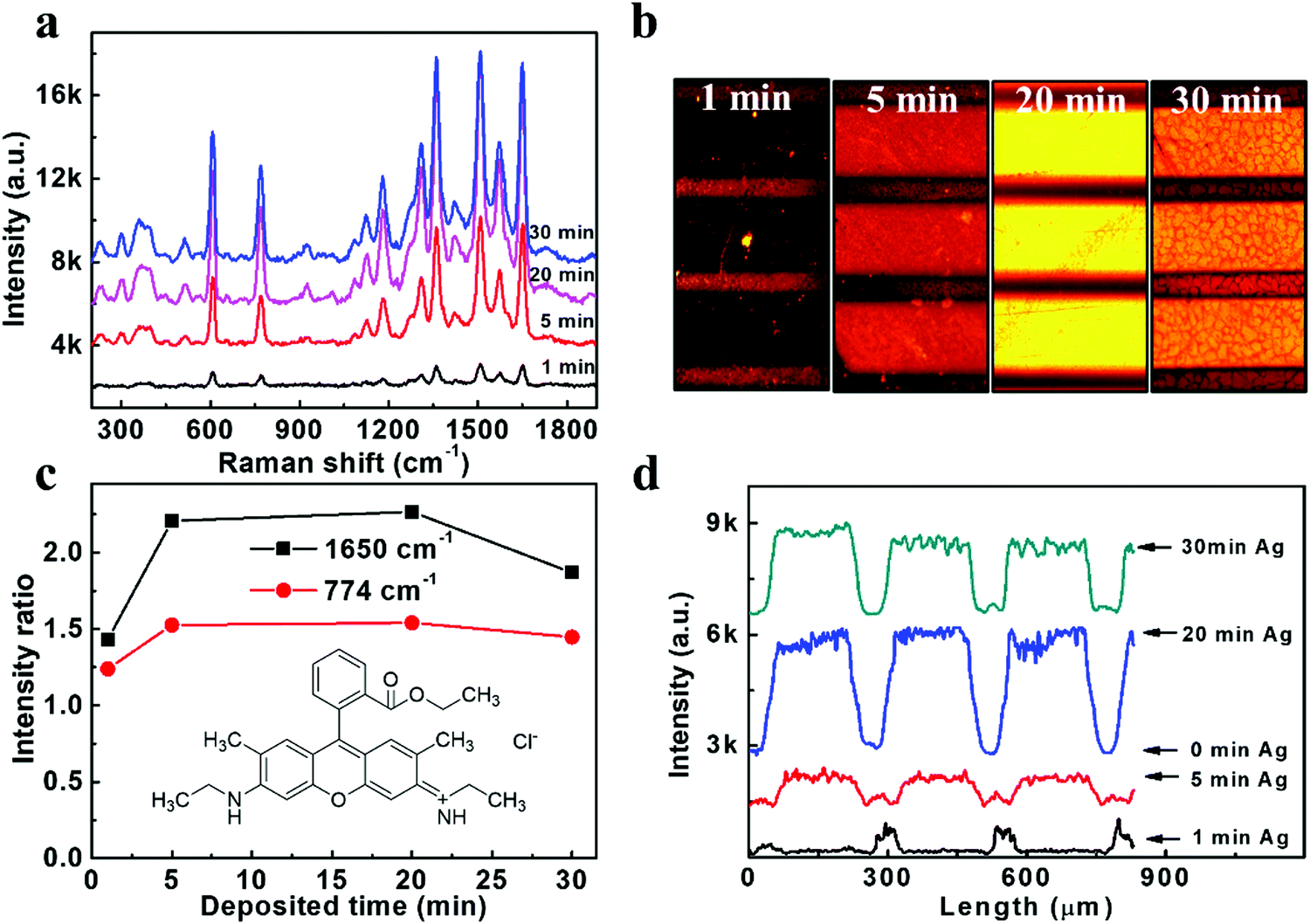 | ||
| Fig. 2 (a) A series of Raman spectra obtained from 1 μM aqueous solutions of R6G molecules absorbed on the as-prepared Ag/ZnO NRs and (c) the calculated intensity ratios of the Raman peaks at 1650 cm−1 and 774 cm−1; the inset shows the structure of the R6G molecule. (b) Fluorescence images of patterned Ag/ZnO NRs with Ag deposition durations of 1 min, 5 min, 20 min, and 30 min, and (d) the corresponding fluorescence-intensity distributions. | ||
Furthermore, we would like to investigate the MEF effect of this highly efficient SERS substrate based on Ag/ZnO NRs. Specifically, patterned templates were fabricated using a copper grid as the mask for MEF observation during the Ag decorating process. As shown in Fig. S4 (ESI†), the broad domains (200 μm in width) and the narrow stripes (50 μm in width) represented the Ag/ZnO NRs and bare ZnO NRs, respectively. The fluorescence images were obtained under excitation centered at 530 nm using a fluorescence microscope and further analyzed by Image J software. As shown in Fig. 2(b), the fluorescence was quenched on the 1 min Ag/ZnO NR platform, indicating that the 1 min Ag/ZnO NRs are insufficient to enhance the fluorescence intensity of R6G, which could be attributed to the non-radiative energy transfers to the metal grains from the excited state of the molecules when they directly contact with each other.13 However, we found that this quenching effect was overcome when the deposition time of the Ag NPs was increased to 5–30 min. The enhancement factors were further calculated according to the corresponding fluorescence intensity exhibited in Fig. 2d. The fluorescence intensities obtained from the Ag/ZnO zones with 1 min, 5 min, 20 min, and 30 min Ag decoration time were about 1/4, 6, 16 and 12-fold that of the ZnO NRs, respectively. The most robust fluorescence enhancement platform is also the 20 min Ag/ZnO, the same as the SERS cases. The fluorescence detection limit of R6G dyes was also analyzed on the 20 min Ag/ZnO NRs. The fluorescence images and corresponding intensity of the R6G dyes (Fig. S5, ESI†) demonstrated that the lowest detection limit of R6G dyes is 100 fM. These results proved that the Ag/ZnO NRs could be used as a reliable platform for SERS and MEF dual-functional detection.
Electromagnetic mechanisms
To get more insights into the mechanisms of the SERS-MEF dual enhancement based on the 3D Ag/ZnO NRs, and especially to understand the phenomenon from quenching for 1 min Ag/ZnO to enhancement for 5 min Ag/ZnO in MEF detection, finite-difference time-domain (FDTD) simulations were carried out to study the spatial distribution of local electromagnetic (EM) fields using the RF Module of COMSOL Multiphysics software. According to the SERS experiments, Fig. 3 illustrates the electric field intensity distribution calculated at the surface of two coupled composited NRs under perpendicular irradiation with a wavelength of 532 nm. The initial electric field amplitude of the incident light was assumed to be |E0| = 1, and k indicates the propagation direction. For 1 min Ag/ZnO, a typical model had 6 nm Ag NP-decorated 70 nm diameter ZnO NRs. The interparticle spacing of 10 nm and inter-rod spacing of 90 nm were built in Fig. 3a according to the TEM image in Fig. 1b. For 5 min Ag/ZnO, a typical model had 25 nm Ag NP-decorated 70 nm diameter ZnO NRs, and the interparticle spacing of 2 nm and inter-rod spacing of 90 nm were built in Fig. 3b according to the TEM image in Fig. 1e. As shown in Fig. 3a, for 1 min Ag/ZnO, the main EM field intensity occurred only near the metallic Ag NPs at a short distance of several nanometers through the local field enhancement effects. However, for 5 min Ag/ZnO, besides the EM field near the metallic Ag NPs, there were other strong enhanced EM fields close to the Ag NP-to-Ag NP junctions, which were not only located surrounding the top or side surface of a single rod, but also located between the Ag NPs on the sidewall of two adjacent ZnO NRs. In addition, the strongest EM field appeared at the Ag NP-to-ZnO NR junction. These enhanced fields can benefit enhancing the detection signal of the analytes, which were absorbed in gaps of the inter-ZnO NRs. In these regions, the strongly localized plasmons yielded from the excited Ag NPs could lead to strong local field enhancements, largely enhancing the Raman scattering and fluorescence signals. Furthermore, the local field enhancement factor confined in the nanogaps were estimated by |Eloc|2/|E0|2,28 where E0 indicates the magnitude of the electric field of the incident light in a linear simulation, calculated in the air as 4.4 × 10⁴, and E is the local maximum electric field with a calculated value of 2.3 × 10⁵ for 1 min Ag/ZnO and 1.0 × 10⁶ for 5 min Ag/ZnO. Then the estimated |Eloc|2/|E0|2 of 5 min Ag/ZnO (6.25 × 10²) is over 22 fold that of the 1 min Ag/ZnO (2.7 × 101). As a result, for 1 min Ag/ZnO NRs, the electrical field enhancement is not efficient to overcome the fluorescence quenching effect due to the non-radiative energy transfer between the metal and fluorophore, resulting in a quenching effect of the fluorescence. However, when increasing the Ag sputtering time to 5 min, the much stronger local field-enhancement around the Ag NPs and between two ZnO NRs can effectively overcome the fluorescence quenching effect to enhance the fluorescence emission (Fig. 2b).29,30 Therefore, the strong localized electrical field of the 3D Ag/ZnO nanostructures plays a significant role in determining the fluorescence and SERS enhancement effect.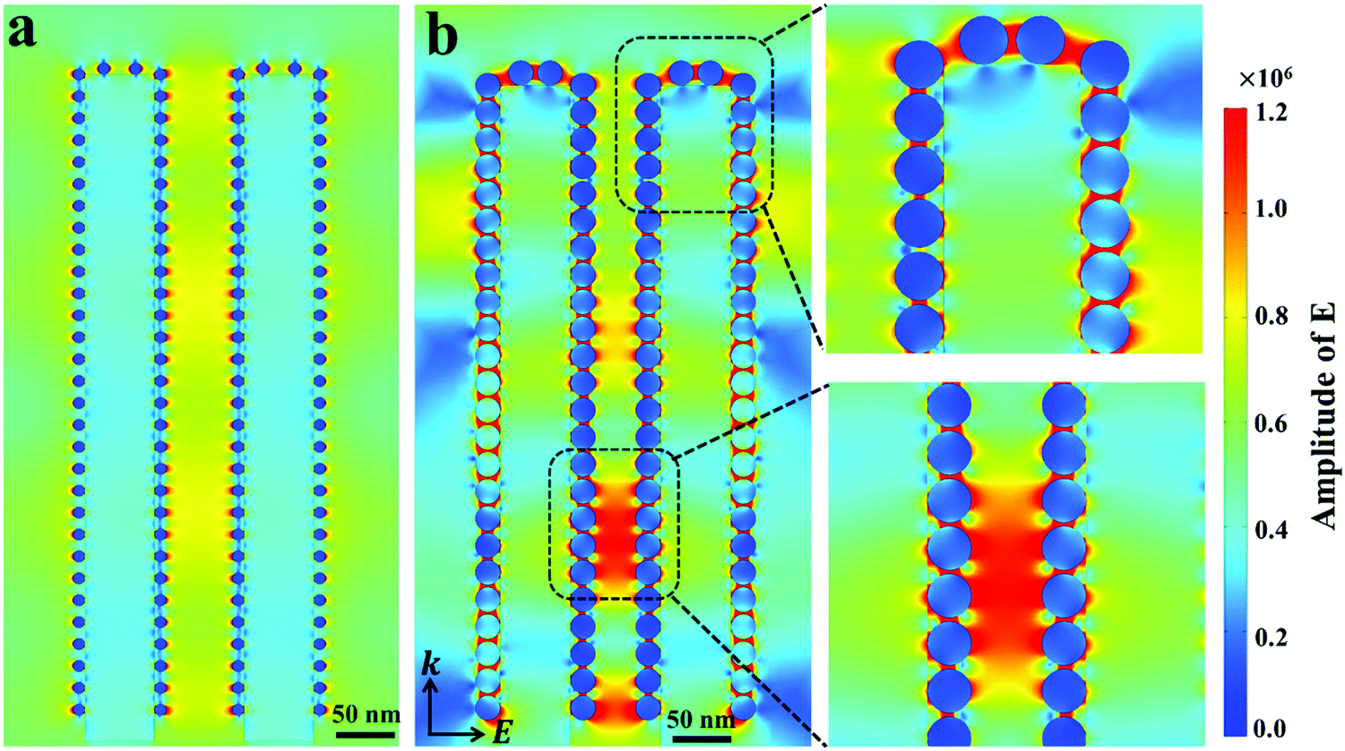 | ||
| Fig. 3 Electric field density distributions for (a) 1 min and (b) 5 min Ag/ZnO NRs using FDTD simulations. | ||
Conclusions
This work developed the robust 3D nanostructure of Ag NPs/ZnO NRs to enhance SERS and fluorescence responses simultaneously. The ultrasensitive detection of Rhodamine 6G dye molecules at extremely low detection limits of 10 fM for SERS and 100 fM for MEF can be achieved. We found that the EM enhancement field can overcome the quenching effects in MEF to enhance the fluorescence intensity of R6G fluorescence, even with direct contact with the Ag NPs, which was supported by FDTD simulations. Our work could be further adapted for ultrasensitive and reliable biomarker detection.Experimental
Fabrication of the ZnO seed layer
The ZnO seed layer was first prepared on a Si substrate by sputtering the ZnO target through the radio-frequency (RF) magnetron sputtering method. The deposition conditions are: the RF power of 150 W, the working pressure of 1 Pa with argon gas and oxygen gas at the flow rate of 40 sccm (standard-state cubic centimeter per minute) and 10 sccm, the sputtering time of 2 min, and the temperature fixed at 400 °C.Preparation of ZnO nanorod arrays
ZnO nanorod arrays were synthesized by a hydrothermal process on ZnO seed layers. Equimolar aqueous solutions (50 mL, 0.1 M) of zinc nitrate hexahydrate (Zn(NO3)2·6H2O, 99%, Aladdin, China) and hexamethylenetetramine (HMT, C6H12N4, 99%, Aladdin, China) were separately prepared in glass bottles and then maintained at 90 °C to get thermal stability. The solutions were mixed, and the ZnO seeded Si substrates were subsequently immersed in reactive solutions. The glass bottles were then sealed and maintained at 90 °C for 3 hours. After growth, the nanorod samples were cleaned by rinsing in deionized water and ethanol, and then dried in air.Decoration of Ag NPs on the ZnO nanorod arrays
Ag NPs were decorated onto the ZnO NRs by magnetron sputtering at room temperature. Striped copper transmission electron microscopy grids (100 meshes) were employed as masks and attached to the ZnO NR platform to obtain patterned substrates. After decoration, the masks were removed from the resultant samples. The sputtering conditions are: the RF power of 40 W, the working pressure of 1 Pa with argon gas at the flow rate of 40 sccm, and the deposition times of 1, 5, 20, and 30 min, respectively.Characterization
The crystallinity and surface morphologies of the samples were characterized by X-ray diffractometer (XRD) (PANalytical, X’Pert Pro) with Cu Kα radiation (λ = 1.54 Å), field emission scanning electron microscopy (FESEM) (FEI Quanta 200 F, 30 kV), transmission electron microscopy (TEM) and high-resolution transmission electron microscopy (HRTEM) (TecnaiG2F30, 300 kV).Evaluation of the fluorescence and Raman performances
The as-prepared Ag/ZnO nanorods were immersed in 1 mL R6G solutions of different concentrations at 4 °C for 12 h. After that, the samples were washed with deionized water and dried in the air. The fluorescence images of the samples were taken by a fluorescence microscope (Leica DM4000 B) using excitation light at 530 ± 20 nm and exposed for 1 s. All obtained fluorescence results were quantitatively analyzed by the Leica AF software. SERS spectra of different samples modified with the R6G fluorophore at different concentrations were collected under the same conditions by a LabRAM XploRA laser Raman spectrometer (HORIBA Jobin Yvon CO. Ltd) using a laser line of 532 nm.Raman bands of R6G molecules
The Raman bands at 1650, 1577, 1509, 1420, 1363, 1312, 1183, and 1127 cm−1 are assigned to armo C–C stretching vibrations, and among these strong peaks, those at 1420, 1363, and 1312 cm−1 can also be attributed to C–N stretching, and those at 1183 cm−1 and 1127 cm−1 belong to C–H in-plane bending. The band at 1276 cm−1 belongs to C–O–C stretching, those at 1087, 930, and 774 cm−1 are assigned to C–H out-of-plane bending, the bands at 662 and 611 cm−1 are assigned to C–C–C ring in-plane bending, and those at 268 and 518 cm−1 are attributed to torsional and/or bending (ring).Conflicts of interest
The authors declare no competing interests.Acknowledgements
This work was supported by the Excellent Youth Project of Heilongjiang Natural Science Foundation (Grant no. JJ2019YX0314), University Nursing Program for Young Scholars with Creative Talents in Heilongjiang Province (Grant no. UNPYSCT-2018185), the National Natural Science Foundation of China (Grant no. 11747166), the Fundamental Research Funds for the Central Universities (Grant no. 2017-KYYWF-0144), and the National Natural Science Foundation of China (Grant no. 51772066, 52073074).References
- H. B. Cheng, Y. Li, B. Z. Tang and J. Yoon, Chem. Soc. Rev., 2020, 49, 21–31 RSC.
- T. Xu, L. P. Xu, X. Zhang and S. Wang, Chem. Soc. Rev., 2019, 48, 3153–3165 RSC.
- Y. Fan, S. Wang and F. Zhang, Angew. Chem., Int. Ed., 2019, 58, 13208–13219 CrossRef CAS PubMed.
- D. Jimenez de Aberasturi, M. Henriksen-Lacey, L. Litti, J. Langer and L. M. LizMarzán, Adv. Funct. Mater., 2020, 30, 1909655 CrossRef CAS.
- Y. Xie, S. Yang, Z. Mao, P. Li, C. Zhao, Z. Cohick, P.-H. Huang and T. J. Huang, ACS Nano, 2014, 8, 12175–12184 CrossRef CAS PubMed.
- H. Tang, G. Meng, Q. Huang, Z. Zhang, Z. Huang and C. Zhu, Adv. Funct. Mater., 2012, 22, 218–224 CrossRef CAS.
- A. K. Pal, C. J. Chandra, S. Umapathy and D. B. Mohan, J. Appl. Phys., 2020, 127, 164501 CrossRef CAS.
- S. Cui, Z. Dai, Q. Tian, J. Liu, X. Xiao, C. Jiang, W. Wu and V. A.-L. Roy, J. Mater. Chem. C, 2016, 4, 6371–6379 RSC.
- A. K. Pal, S. Pagal, K. Prashanth, G. K. Chandra, S. Umapathy and D. B. Mohan, Sens. Actuators, B, 2019, 279, 157–169 CrossRef CAS.
- H. K. Lee, Y. H. Lee, C. S.-L. Koh, G. C. Phan-Quang, X. Han, C. L. Lay, H. Y.-F. Sim, Y. C. Kao, Q. An and X. Y. Ling, Chem. Soc. Rev., 2019, 48, 731–756 RSC.
- Y. Jeong, Y. M. Kook, K. Lee and W. G. Koh, Biosens. Bioelectron., 2018, 111, 102–116 CrossRef CAS PubMed.
- J. Langer, D. Jimenez de Aberasturi, J. Aizpurua, R. A. Alvarez-Puebla, B. Auguie, J. J. Baumberg, G. C. Bazan, S. E.-J. Bell, A. Boisen, A. G. Brolo, J. Choo, D. Cialla-May, V. Deckert, L. Fabris, K. Faulds, F. J. Garcia de Abajo, R. Goodacre, D. Graham, A. J. Haes, C. L. Haynes, C. Huck, T. Itoh, M. Kall, J. Kneipp, N. A. Kotov, H. Kuang, E. C. Le Ru, H. K. Lee, J. F. Li, X. Y. Ling, S. A. Maier, T. Mayerhofer, M. Moskovits, K. Murakoshi, J. M. Nam, S. Nie, Y. Ozaki, I. Pastoriza-Santos, J. Perez-Juste, J. Popp, A. Pucci, S. Reich, B. Ren, G. C. Schatz, T. Shegai, S. Schlucker, L. L. Tay, K. G. Thomas, Z. Q. Tian, R. P. Van Duyne, T. Vo-Dinh, Y. Wang, K. A. Willets, C. Xu, H. Xu, Y. Xu, Y. S. Yamamoto, B. Zhao and L. M. Liz-Marzan, ACS Nano, 2020, 14, 28–117 CrossRef CAS PubMed.
- E. Petryayeva and U. J. Krull, Anal. Chim. Acta, 2011, 706, 8–24 CrossRef CAS PubMed.
- R. A. Alvarez-Puebla, N. Pazos-Perez and L. Guerrini, Appl. Mater. Today, 2018, 13, 1–14 CrossRef.
- M. Tavakkoli Yaraki, S. Daqiqeh Rezaei and Y. N. Tan, Phys. Chem. Chem. Phys., 2020, 22, 5673–5687 RSC.
- S. Chang, S. L. Eichmann, T.-Y. S. Huang, W. Yun and W. Wang, J. Phys. Chem. C, 2017, 121, 8070–8076 CrossRef.
- R. Gill, L. Tian, W. R.-C. Somerville, E. C. Le Ru, H. van Amerongen and V. Subramaniam, J. Phys. Chem. C, 2012, 116, 16687–16693 CrossRef CAS.
- A. M. Gabudean, M. Focsan and S. Astilean, J. Phys. Chem. C, 2012, 116, 12240–12249 CrossRef CAS.
- R. Gill, L. Tian, W. R.-C. Somerville, E. C. Le Ru, H. van Amerongen and V. Subramaniam, J. Phys. Chem. C, 2012, 116, 16687–16693 CrossRef CAS.
- W. Yao, L. Chang, W. Yin, T. Wang, Y. Yang, P. Yin, M. Yang, Y. Ma, Y. Qin and H. Ma, Spectrochim. Acta, Part A, 2019, 223, 117303 CrossRef CAS PubMed.
- Y. Zhang, G. Zhang, P. Yang, B. Moosa and N. M. Khashab, ACS Appl. Mater. Interfaces, 2019, 11, 27529–27535 CrossRef CAS PubMed.
- Y. Yin, Y. Sun, M. Yu, X. Liu, T. Jiang, B. Yang, D. Liu, S. Liu and W. Cao, Sci. Rep., 2015, 5, 8152 CrossRef CAS PubMed.
- B. Du, C. Tang, D. Zhao, H. Zhang, D. Yu, M. Yu, K. C. Balram, H. Gersen, B. Yang, W. Cao, C. Gu, F. Besenbacher, J. Li and Y. Sun, Nanoscale, 2019, 11, 14322–14329 RSC.
- P. Hildebrandt and M. Stockburger, J. Phys. Chem., 1984, 88, 5935–5944 CrossRef CAS.
- G. Barbillon, Coatings, 2019, 9, 86 CrossRef.
- D. T. Tieu, T. N. Quynh Trang, L. V. Tuan Hung and V. T. Hanh Thu, J. Alloys Compd., 2019, 808, 151735 CrossRef CAS.
- L. Lu, J. Zhang, L. Jiao and Y. Guan, Nanomaterials, 2020, 9, 916 CrossRef PubMed.
- S. Y. Ding, E. M. You, Z. Q. Tian and M. Moskovits, Chem. Soc. Rev., 2017, 46, 4042–4076 RSC.
- R. Gill and E. C. Le Ru, Phys. Chem. Chem. Phys., 2011, 13, 16366–16372 RSC.
- E. Kohr, B. I. Karawdeniya, J. R. Dwyer, A. Gupta and W. B. Euler, Phys. Chem. Chem. Phys., 2017, 19, 27074–27080 RSC.
Footnote |
| † Electronic supplementary information (ESI) available. See DOI: https://doi.org/10.1039/d2ma00368f |
| This journal is © The Royal Society of Chemistry 2022 |