
 Open Access Article
 This Open Access Article is licensed under a
 Creative Commons Attribution 3.0 Unported Licence
Elucidation of the mechanism for maintaining ultrafast domain wall mobility over a wide temperature range†
S.
Ranjbar
 *a,
S.
Kambe
a,
S.
Sumi
a,
P. V.
Thach
ab,
Y.
Nakatani
c,
K.
Tanabe
a and
H.
Awano
a
*a,
S.
Kambe
a,
S.
Sumi
a,
P. V.
Thach
ab,
Y.
Nakatani
c,
K.
Tanabe
a and
H.
Awano
a
aToyota Technological Institute, Nagoya 468-8511, Japan. E-mail: sina.ranjbar@toyota-ti.ac.jp
bInstitute of Materials Science, Vietnam Academy of Science and Technology, 18 Hoang Quoc Viet, Hanoi, Vietnam
cGraduate School of Informatics and Engineering, University of Electro-Communications, Chofu, Tokyo 182-8585, Japan
First published on 29th July 2022
Abstract
To achieve a 20 Gbps data rate using the upcoming 5G communication standard, it is crucial to recognize a domain wall (DW) velocity (vDW) of 1200 m s−1. We demonstrate a potential means of achieving the DW speed of 1200 m s−1 at low current density in a wide temperature range from 270 to 350 K in Fe-rich GdFeCo magnetic wire. We show a significant relationship between the vDW and the pulse duration width, which corresponds to the Joule heating effect and the shape of the DW. Generally, if the current density is constant, the current-driven DW displacement is proportional to the pulse width, so the DW speed is also constant. We found that the vDW increases with the shortening of the applied pulse current width. However, the DW shape appears rounded in the case of long pulse duration width. Accordingly, the damping-like effective field and the Neel DW are not orthogonal to each other except in the wire center; as the efficiency of SOT decreases, the DW speed reduces. We also measured the Dzyaloshinskii–Moriya interaction (DMI) field for 3 ns 30 ns pulse duration widths. In the case of 30 ns, the DMI field was found halved in comparison to the 3 ns width. Generally, the DMI field is a material-specific parameter, and this difference is clarified by the shape of the DW driven by the current. Our findings on the fast and high thermal stability of DW motion at low current density in compensated ferrimagnetic material open new opportunities for high-speed spintronic devices.
1. Introduction
Spintronics applications are extensively investigated for high-performance logic computing technologies and racetrack memories.1–4 In the past decade, most studies have focused on thin ferromagnetic films deposited on a heavy metal, where the interfacial Dzyaloshinskii–Moriya interaction (DMI) stabilizes chiral Neel walls that can be efficiently driven by spin Hall effect-spin orbit torque (SHE-SOT).5–7 In ferromagnetic materials, low coercivity (Hc) is an advantage, however, large critical current density (Jc), bit size, stray field interactions, and precessional dynamics of the operating speeds present substantial limitations.8–10 Recently, current-induced domain wall (DW) motion in ferrimagnets has become an intense field of research. These materials consist of rare-earth (RE) and transition metal (TM) compounds in which the magnetization and angular momentum compensation of the two sublattices may be achieved by adjusting either the temperature or the composition of the material.1,11 Several studies have, in particular, reported that spin-transfer torque,12–14 spin–orbit torque,15 and field-driven 1 DW motion in ferrimagnets are fastest at the angular momentum compensation temperature (TAMC), where the magnetic dynamics are antiferromagnetic. Several reports have predicted that the fast current-induced DW motion (CIDWM) appears near the angular momentum compensation temperature for ferrimagnetic wires.1,11,16 However, some principal difficulties faced in this situation are reaching small bits,17 high thermal stability, and track of these parameters without using an in-plane external magnetic field at high speed.18 To overcome this challenge, an alternative strategy is using amorphous rare earth transition metals (RE-TM) ferrimagnetic systems, such as GdFeCo. In this study, we note that Fe concentration is much higher than that of Co in TM, so the GdFeCo is closer in composition to GdFe than it is to GdCo. Many reports have considered that for GdCo to achieve fast DWM, it is essential to apply an external in-plane magnetic field16 as compared to the GdFeCo magnetic wire.Furthermore, we compared our work with previous reports (Table 1). These results have motivated us to analyze the mechanism of DW motion in compensated ferrimagnet. We performed systematic experiments for CIDWM in Gdx(Fe88Co12)100−x ferrimagnetic wires. We have demonstrated that by employing the Gd–FeCo magnetic wire, the DW velocity reaches 1200 m s−1 in a wide range of temperatures from 270 to 350 K when a short pulse duration width is injected into the wire. We then analyzed theoretically and experimentally the temperature dependence of the magnetic wire by applying different pulse duration widths and found that the long pulse duration width generates a more significant temperature gradient than the shorter pulse duration width. We performed experimental and theoretical simulations to clarify the mechanism of DW velocity for various pulse duration widths. At 3 ns, the shape of the DW was orthogonal to the magnetic wire, and a Neel wall was formed in the direction of the magnetic wire. When the damping-like effective field and the Neel DW are orthogonal to each other, hence SOT is efficiently generated and a high DW speed is realized. However, this observation was opposite to the results obtained in the case of 30 ns width. Finally, by observing the DW shape with the inclusion of DMI effects, we identified the origin of the difference in DW speed for short and long pulse duration widths.
| Parameters | TbCo | GdCo | GdFeCo (our results)* |
|---|---|---|---|
| DW speed (m s−1) (room temperature) | 75 | 850 | 1500* |
| J (A m−2) | 3.0 × 10¹¹ | 2.0 × 10¹² | 1.7 × 10¹¹* |
| DW mobility | 5 | 6.5 | 88* |
| Thermal stability (vDW = 1200 m s−1) | No report | Not stable | Stable* |
| g (Re)23–25 | g Tb ∼ 1.5 | g Gd ∼ 2.0 | g Gd ∼ 2.0 |
| g (TM)23–25 | g Co ∼ 2.22 | g Co ∼ 2.22 | g Fe88Co12 ∼ 2.08* (gFe ∼ 2.06; gCo ∼ 2.22) |
2. Experimental section
2.1. Sample preparation
A series of Pt (5)/Gdx(Fe88Co12)100−x(20)/SiN(10) films were deposited by dc magnetron sputtering under an Ar pressure of 0.2 Pa after the chamber was evacuated to a base pressure of about 2 × 10⁻⁸ torr. Here, the 5 nm-thick Pt underlayer performed as a spin current source induced by the spin Hall effect (SHE), providing a spin–orbit torque (SOT). To prevent oxidization, a 10 nm-thick SiN layer was fabricated at the top of the GdxFeCo100−x layer. Here, the 5 nm-thick Pt underlayer performed as a spin current source induced by the spin Hall effect (SHE), providing a spin–orbit torque (SOT). The GdFeCo alloy layers were deposited by co-sputtering FeCo and Gd targets at room temperature. The magnetic wires (3 μm wide and 125 μm long) and Hall crosses were micro-fabricated by an electron-beam lithography (EBL) system and a lift-off method.2.2. Magnetic measurements
The composition of Gd and FeCo can be controlled by controlling the sputtering power. The composition of the films was measured by energy dispersive X-ray analysis (EDX). The Polar-magneto-optical Kerr effect (PMOKE) and vibrating sample magnetometer (VSM) measured the magnetic properties at room temperature. We measured the DW velocity in the GdFeCo wires by applying single voltage pulses (picoseconds) and then observed the DW motion using a Kerr microscope. The velocity of the DW was determined by dividing the change in the position of the DW (as viewed by the polar-magneto-optical Kerr effect (PMOKE)) by the duration of the current pulse (Fig. 2(c)). Note that all measurements were performed at room temperature.3. Results and discussions
3.1. Design and sample characterization
We initially discerned the magnetic properties of Gdx(Fe88Co12)100−x films. Fig. 1(a) exhibits the hysteresis loops that were measured using the PMOKE at room temperature. The polarity of the changes in Kerr rotation (θK) signals between Gd24(Fe88Co12)76 and Gd25(Fe88Co12)75 samples was consistent with a transition from being FeCo-dominated to being Gd-dominated in the magnetic moment. Fig. 1(b) shows the Ms and Hc of deposited Gdx(Fe88Co12)100−x films at different compositions. The saturation magnetization (Ms) of Gdx(Fe88Co12)100−x reached its magnetization compensation composition at (xMC) ∼24 at%. While the Ms was minimum, the coercive fields reached their maximum at magnetic compensation composition.19,20 The angular momentum compensation composition (xAMC) was determined using the following equations:| M = MGd + MFeCO | (1) |
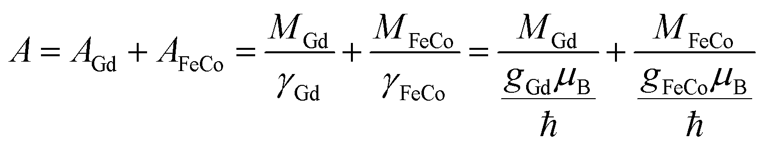 | (2) |
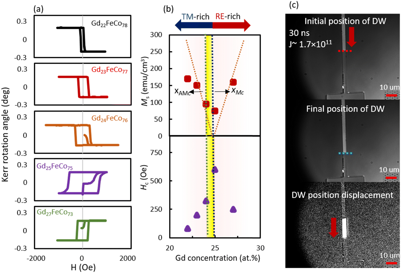 | ||
| Fig. 1 (a) MOKE measurements as a function of perpendicular magnetic field for GdxFeCo100−x films at room temperature. (b) Saturation magnetization and coercivity as a function of Gd composition. (c) Configuration of domain wall (DW) motion in GdxFeCo100−x wire with consecutive current pulses. A large external magnetic field along the out-of-plane was applied to saturate the magnetization and generate an up-down and/or down-up DW to initiate DW propagation from the large contact pad area. The position of DW was displaced before and after applying a pulse current. Red and blue dotted lines show the initial and the final position of DWs in the PMOKE image. The DW motion took place in the direction of the injected current. | ||
3.2. Current-induced domain wall motion
Fig. 2(a–e) shows the dependence of DW velocity as a function of current density for Pt/Gdx(Fe88Co12)100−x/SiN wires (20 < x < 28) measured with a pulse duration of 30 and 3 ns, respectively. In our study, the DW moved along the direction of the pulse current, which can be supported by the spin–orbit torque (SOT) in the heavy metal/ferrimagnet system.5,7Fig. 2(a–e) shows that the DW velocity increased by raising the J for all Gdx(Fe88Co12)100−x compositions. To exclude the contributions from differences in threshold current densities between samples, we concentrated on the flow region where the velocity and the current density approximately satisfied a linear relationship. It must be noted that a Walker breakdown phenomenon was not observed in this system. Besides, the maximum DW velocity, i.e., vDW = 2000 m s−1, was observed with a sample of Gd24(Fe88Co12)76 for 3 ns pulse duration without the application of an in-plane external magnetic field, which is the fastest DW velocity yet in comparison with the previous reports.8,15,16 Consequently, the method using an in-plane external magnetic field cannot be used practically, because it causes data destruction.1,15,16,23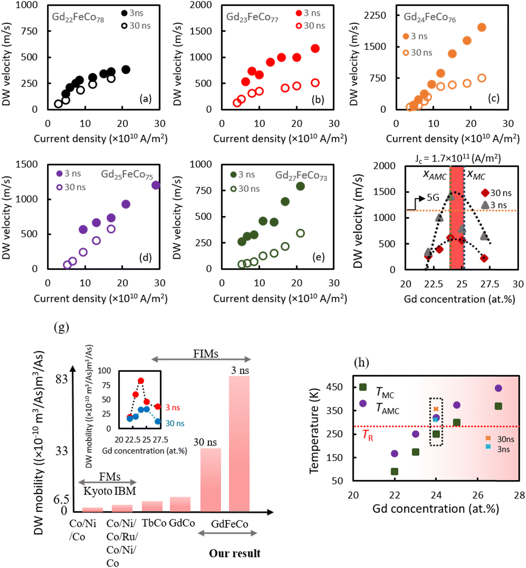 | ||
| Fig. 2 (a–e) Domain wall (DW) velocity as a function of the current density with pulse duration of 30 ns for GdxFeCo100−x/SiN wires (20 < x < 28), (f) DW velocity as a function of current density with pulse duration 30, 3 ns for GdxFeCo100−x/SiN wires (20 < x < 28), (g) a comparison of DW mobility in our study with other reports, (h) summary of TM and TAM as a function of Gd concentration. The TAMC was ∼310 K for the Gd24FeCo76 sample. | ||
Fig. 2(f) demonstrates that DW velocity is a function of Tb and Gd concentration. So far, we have reported many papers on the current-driven DW motion of TbCo magnetic wires, but the DW velocity was as slow as 100 m s−1 or less even if the composition and structure were changed.4,15,24 The maximum DW velocity, i.e., vDW = 1500 m s−1 (>20 Gbps), appears at xAMC point for Gd24(Fe88Co12)76 with a short pulse current of 3 ns width.
To achieve a fast data rate of 20 Gbps, both the low current density (J) and fast DW motion are required. Therefore, large DW mobility, vDW/J, is an important parameter. Upon the comparison of our work with previous reports, it was clear that the DW mobility in the GdFeCo sample is much higher than that of other FM and FIM materials as shown in Fig. 2(h).5,7,8,11,15 The DW mobility for 30 and 3 ns pulse widths was 33 × 10−10 m3 A−1 s−1 and 88 × 10−10 m3 A−1 s−1. These results open a new window for technology to design a new type of racetrack memory that has low power consumption and high-velocity thermal stability.
In Gd24(Fe88Co12)76 with 30 ns pulse width, we observed a non-linear relationship between DW velocity and current density shown in Fig. 2(c). To clarify the J dependence of DW velocity, we first determined the TMC of the Gdx(Fe88Co12)100−x wires using the hysteresis loops at various temperatures (as shown in the Fig. S2, ESI†). Using TMC, the TAMC was evaluated from eqn (S1)–(S4) of the ESI.† In agreement with previous reports, the DW velocity increases near the TAMC.1,11Fig. 3(h) shows that the TMC (green dots) and TAMC (violet dots) are different for each Gdx(Fe88Co12)100−x composition. By increasing the Gd concentration, TMC (green dots) and TAMC (violet dots) shifted toward the higher temperature.
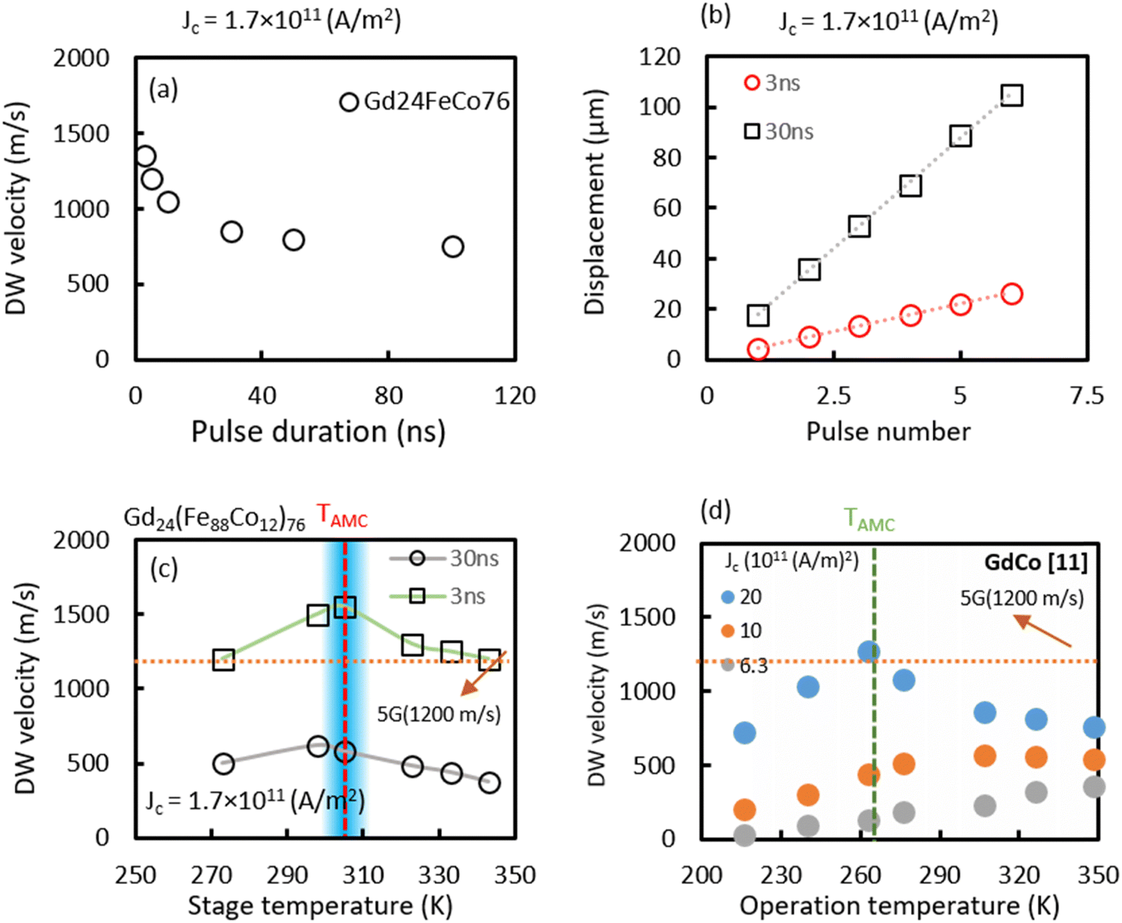 | ||
| Fig. 3 (a) The domain–wall (DW) velocity as a function of pulse duration; the inset shows DW displacement as a function of pulse number, the V30nsDW < V30nsDW, (b) shows that when the pulse width was fixed, and the number of pulses was increased, the DW displacement distance was proportional to the number of pulses, (c and d) temperature dependence measurement for GdCo (MIT result) and GdFeCo magnetic wire (our result). The open squares (black) show our experimental results, while the colored circles denote previous work.11 The highlighted part shows the industrial-grade wide temperature for memory applications. | ||
Since an electric current was applied to the magnetic wire at room temperature, TAMC should present near room temperature to achieve a high DW velocity. It can be considered that the DW velocity of Gd24(Fe88Co12)76 was the fastest in Fig. 2(f) because it met this condition. Joule heat generation25,26 can be taken into account by applying a pulse current, nevertheless the longer the pulse width (30 ns), the higher the Joule heat generation. When the pulse width was 3 ns, the Joule heat generation was small, and the temperature of the magnetic wire was close to TAMC as shown by the blue cross mark in Fig. 2(h). Therefore, it is seen that the DW velocity of the Gd24(Fe88Co12)76 indicates the highest for 3 ns pulse duration width. On the other hand, when the pulse width was 30 ns, it was considered that the temperature of the magnetic wire had risen to the vicinity of the orange cross mark in Fig. 2(h). Therefore, the DW velocity was demonstrated to be the slowest for the 30 ns pulse duration width. In consequence, when the temperature of the magnetic wire was near the TAMC, the DW velocity became faster and showed a linear tendency. On the other hand, when the pulse duration width increased, the temperature exceeded the TAMC, therefore, the DW velocity slowed down. Martínez et al. observed that the T = TAMC relationship between the DW velocity and the current became linear. They also observed a threshold in the case of T > TAMC.27 Therefore, it was seen that the threshold in Gd24(Fe88Co12)76 at 30 and 3 ns corresponded to T > TAMC and T = TAMC, respectively. Therefore, the fast DW motion with linear dependency on the current density was obtained at 3 ns for Gd24(Fe88Co12)76, which corresponds to the theoretical report.
3.3. Pulse duration width dependence on the domain wall motion
As discussed previously, the temperature can affect the magnetic properties of ferrimagnetic materials.25Fig. 3(a) shows the DW velocity as a function of pulse duration for the Gd24(Fe88Co12)76 magnetic wire. Similarly, fixing the current density and increasing the pulse width should increase the DW displacement. However, when the current density was fixed (J =1.7 × 10¹¹ A m−2) and the pulse width was increased as shown in Fig. 3(a), the DW velocity became slower, contrary to the expectation; this expectation could be explained due to the Joule heating effect in the Gd24(Fe88Co12)76 magnetic wire. It is well known that the effect of Joule heating on the DW velocity can be clarified as follows: When the applied current flows through the magnetic wire, the temperature in the Gd24(Fe88Co12)76 layer rises, depending on the pulse duration. However, increasing the sample temperature with a higher pulse current duration drives the sample away from the compensation region, and the DW velocity decreases. By fixing the pulse width at 3 and 30 ns, the number of pulses increases, and the DW displacement distance was ideally proportional to the number of pulses as shown in Fig. 3(b). The effect of the pulse duration width on DW velocity was confirmed by temperature dependence measurement for Gd24(Fe88Co12)76 magnetic wire as shown in Fig. 3(c). Fig. 2(h) shows that the TAMC was estimated at 300 K for the Gd24(Fe88Co12)76 magnetic wire. Fig. 3(c) shows that the maximum DW velocity appeared at TAMC for Gd24(Fe88Co12)76 magnetic wire for both short and long pulse duration widths of 3 and 30 ns, respectively.16 It seems that the short pulse duration width of 3 ns retained the sample temperature close to the TAMC, while the long pulse duration width of 30 ns drove the sample away from the TAMC, therefore, the DW velocity decreased. In our system, the change in DW velocity at TAMC was not sharp, as we successfully reduced the input current density about 10 times in comparison to the previous report,11 which is in good agreement with the theoretical model.11,16,28 Consequently, the dependence of DW dynamics on both J and pulse duration width provides an essential strategy for designing racetrack devices based on ferrimagnets using both low energy dissipation and fast operation speed, which is not easy to achieve simultaneously.3.4. Thermal stability of GdFeCo wire
The specification, “industrial-grade wide temperature”, was ordinarily determined by the temperature range of 0 to 55 °C.29 We should note that defining a wide temperature range for industrial memory applications is crucial. In addition, our experimental data shows that fast and stable DW motion occurs in a short pulse current. Fig. 3(d) shows the DW velocity of the Gd24(Fe88Co12)76 as a function of operating temperature for a pulse current of 3 ns as compared with GdCo magnetic wire.11 The DW speed obtained was stable between the temperature range of R.T. < Top < 70 °C for Gd24(Fe88Co12)76 when the pulse current of 3 ns was injected into the magnetic wire. It is noted that Top is the stage temperature that was used for temperature measurements. In addition, for a short pulse current of 3 ns, the DW velocity remained relatively constant over 1200 m s−1 between room temperature and 70 °C, which is suitable for racetrack memories. A short pulse current of 3 ns with low input current density (J ∼ 1011 A m−2) showed a broader and stable peak for ferrimagnetic magnetic wire systems, which was in good agreement with the theoretical model.1,11,13 In the theoretical and experimental model, a sharp peak appeared at TAMC for large input current density (J ∼ 1012 A m−2). However, it can be seen that for small input current density (J ∼ 1011 A m−2), a broad peak appeared around TAMC, while the DW velocity was slow.11 We conclude that fast and stable DW motion in a wide temperature range with low current density (J ∼ 1011 A m−2) was observed in Pt/Gd24(Fe88Co12)76 magnetic wire without the application of an external in-plane magnetic field, which would be suitable for racetrack memory devices.3.5. Discussion
Generally, when the constant current density is applied, the DW displacement is proportional to the application time of the pulse current. This means that the DW speed is constant at any pulse duration. However, we have observed a different result. The DW speed with a pulse width of 3 ns was faster than 30 ns.We performed an experimental and theoretical simulation to clarify the mechanism of DW velocity for various pulse duration widths. The observed polarized optical microscope images are shown in Fig. 4(a and b) for 3 ns and 30 ns pulse duration widths taken at room temperature. Fig. 4(a) shows that the DW shape was straight for a short pulse duration width of 3 ns, while it was rounded for 30 ns pulse duration width as shown in Fig. 4(b). To confirm this finding, we performed a micromagnetic simulation to observe the DW shape for different pulse duration widths as shown in Fig. 4(c–f). Fig. 4(c and d) show the DW shape at the initial state and after injecting a pulse duration of 3 ns, respectively. The DW shape showed a tiny change and a uniform motion when a short pulse duration width of 3 ns was injected into the wire; afterward, the DW presented a straight shape, which was consistent with our experimental observations. This calculation assumed that the entire magnetic wire had an anisotropic dispersion of 30%. Therefore, homogenous anisotropic dispersion could be driven by an electrical current, while maintaining a straight DW shape at the recording time. However, Fig. 4(e) indicated that if a 30 ns pulse current was continuously applied to the wire, the straight DW structure was disturbed. When the applied current was stopped at 30 ns, a smoothing occurred to reduce the DW energy. The disordered DW structure showed a rounded shape on the right side as shown in Fig. 4(f), which was attributed to the absence of magnetic film outside the wire edge, unevenness of the edge portion, and non-uniformity of the magnetization state. Therefore, the movement of the DW at the edge portion was slow, and the DW was rounded. As a result of the LLG simulation, Fig. 4(e) shows that the displacement of the DW after application of the pulse current was 30 ns, which was only 6 times as compared to that for 3 ns. These observations indicate that if the DW is driving at a constant speed, the displacement should be 10 times longer, however, the result exhibits an increase of merely 6 times. Thus, the DW velocity with a pulse width of 30 ns is about 60% lower than that with 3 ns. As a result, the simulation supports the experimental data that the DW velocity with a pulse width of 30 ns is about half as compared with a pulse width of 3 ns. We infer that the rounded shape of the DW is one of the causes of the slow DW motion for a long pulse duration width. A theoretical study showed that by narrow wire width, we might be able to prevent the round shape of the DW, which is thought to be due to the wide wire width of 3 μm in this experiment as well.30
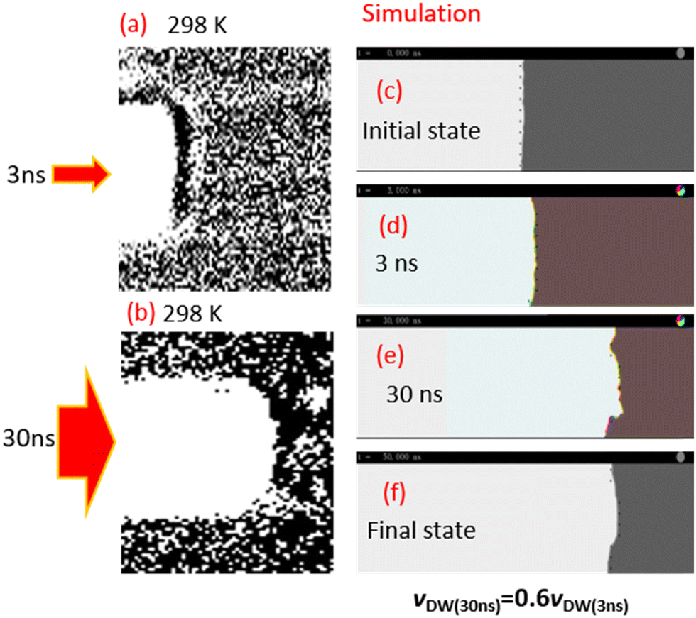 | ||
| Fig. 4 Polarized optical microscope images of current-driven domain wall (DW) shape at room temperature for (a) 3 ns, and (b) 30 ns pulse duration width. Simulation results of DW shape, (c–f) for 3 ns and 30 ns pulse duration width. | ||
To investigate the mechanism leading to this difference in velocity, we schematically illustrate the DW shape in Fig. 5(a and b). At 3 ns, the shape of the DW was orthogonal to the magnetic wire, and a Neel wall was formed in the direction of the magnetic wire, which is schematically shown in Fig. 5(a). Therefore, it is considered that the spin currents flowing from the Pt layer and the Neel wall were orthogonal to each other, so SOT was efficiently generated and a high DW speed was achieved. However, in the case of 30 ns, the DW shape appeared to be rounded. Therefore, it was considered that the damping-like effective field and the Neel DW were not orthogonal to each other as shown schematically in Fig. 5(b), the efficiency of SOT was reduced, and the DW speed was decreased.
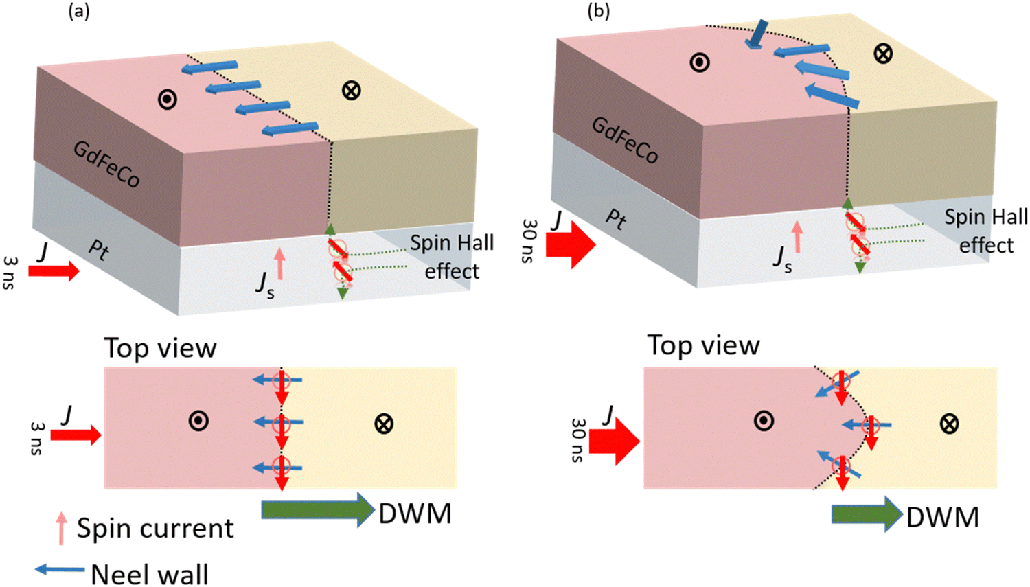 | ||
| Fig. 5 Schematic illustration of the domain wall (DW) shape for (a) 3 ns and (b) 30 ns pulse duration width. | ||
A thermal calculation was performed to determine whether a difference in DW shape was caused by the pulse width as shown in Fig. 6(a). Since it is generally difficult to measure the thermal conductivity of an ultrathin film, the values in the reference paper were used for the thermal conductivity. Therefore, although the absolute value was unknown, the difference in heat distribution between when a pulse width of 30 ns was applied and when the pulse width was 3 ns can be qualitatively discussed.
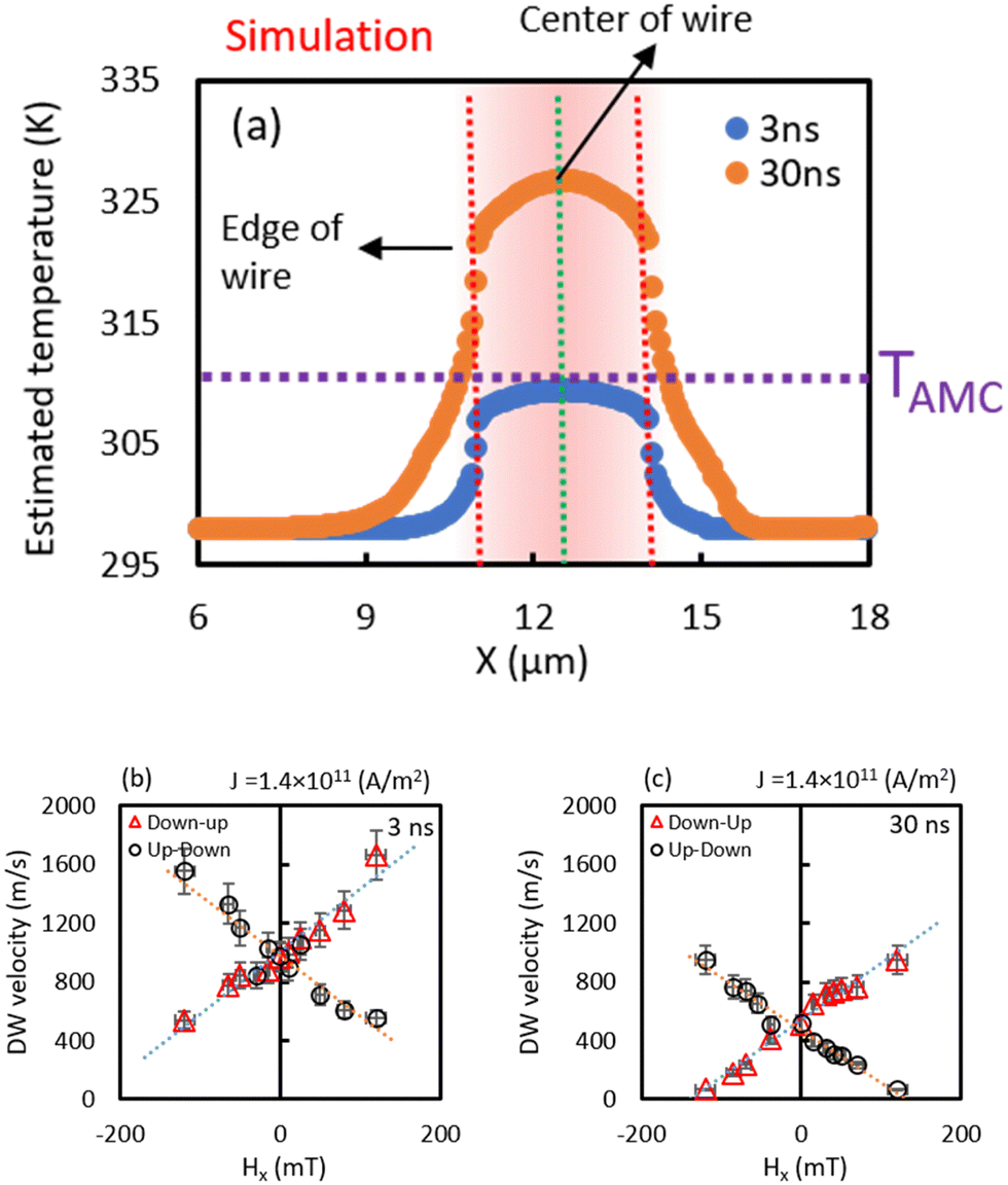 | ||
| Fig. 6 (a) The estimated temperature profile calculation results of the cross-section of the magnetic wire due to the Joule heat when a pulse current was applied to the magnetic wire. The orange dot shows the result of the pulse current application time of 30 ns, and the blue dot shows that of 3 ns. Domain wall (DW) velocity as a function of an external in-plane field (Hx) along the wire for (b) 3 ns and (c) 30 ns pulse duration width. | ||
As can be seen from this calculation result, in the case of a pulse width of 3 ns, the temperature difference between the center of the magnetic wire and the wire edge was small. It was considered that uniform DW motion was achieved at any DW position. On the other hand, in the case of 30 ns, the temperature at the center of the DW was higher than that at the wire edge. Therefore, since the DW energy at the center of the wire was lower than that at the wire edge, the DW at the center of the magnetic wire moved faster than the edge portion. Therefore, it is estimated that the DW shape was rounded. Due to this DW shape, it was considered that the longer the pulse width, the lower the DW moving speed.
The DW shape should affect the DMI magnetic field. Therefore, to obtain a quantitative determination of the effective DMI field (HDMI), we extracted the crossing fields for the 3 and 30 ns pulse widths as shown in Fig. 6(b and c) and summarized in Table 2. We could estimate the interfacial DMI coefficient of our sample for different pulse duration widths using the formula:
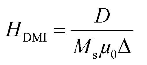 | (3) |
| Pulse duration (ns) | Current density (A m−2) | DW velocity (m s−1) Hx = 0 | DMI field (mT) |
|---|---|---|---|
| 3 | 1.4 × 10¹¹ | 1033 | 243 |
| 30 | 1.4 × 10¹¹ | 528 | 122 |
The DMI ratio and the DW velocity ratio at 3 and 30 ns were doubled, indicating a strong correlation between DMI and DW speed. The inclination in Fig. 6(b and c) is due to the spin Hall effect, but the tendency is the same in both cases. The decisive difference is due to DMI, which is attributable to the shape of the DW driven by the current. These results highlight the unique feature of the effect of the measurement method on current-driven DW motion.
4. Conclusion
In summary, in a compensated ferrimagnetic magnetic wire, we achieved fast DW motion (vDW > 1200 m s−1) in a wide temperature range from 270 to 350 K. We have experimentally demonstrated and theoretically explained that a short pulse current of 3 ns is more stable and faster than a long pulse width of 30 ns. The mechanism leading to the difference in DW speeds was clarified by experimental observation of the DW shape with the inclusion of DMI effects. Therefore, we presented that pulse duration width may be impacted by the DW shape, therefore, at 3 ns, the shape of the DW was orthogonal to the magnetic wire, and a Neel wall was formed in the direction of the magnetic wire. Accordingly, the damping-like effective field and the Neel DW were orthogonal to each other so that SOT was efficiently generated and a fast DW speed was discerned; the pattern was opposite for 30 ns pulse duration width due to the rounded DW wall shape. Therefore, our findings provide a basis for achieving low power and fast speed by choosing the appropriate current pulse density, and thus invigorate research toward the development of memory applications.Data availability statement
Data supporting the findings of this study are available from the corresponding author upon reasonable request.Author contributions
S. R. and H. A. planned the project. S. R. deposited films, fabricated devices, and performed the transport measurements. S. K. and Y. N. performed the theoretical analysis. S. R., S. S., S. K., P. V. T., K. T., and H. A. analyzed the data. All authors discussed the results and commented on the manuscript. S. R. wrote the manuscript. S. R. and H. A. initiated the idea and led the project.Conflicts of interest
The authors declare no conflict of interest.Acknowledgements
The authors acknowledge Dr Ahmet Yagmur and Dr Mohammad Saeed Bahramy for their valuable discussions. We acknowledge funding from JSPS KAKENHI (grants 20H02185, 21K14202).References
- K. J. Kim, S. K. Kim, Y. Hirata, S. H. Oh, T. Tono, D. H. Kim, T. Okuno, W. S. Ham, S. Kim, G. Go, Y. Tserkovnyak, A. Tsukamoto, T. Moriyama, K. J. Lee and T. Ono, Nat. Mater., 2017, 16, 1187–1192 CrossRef CAS PubMed.
- L. T. Stuart, S. P. Parkin and M. Hayashi, Science, 2008, 320, 190–194 CrossRef PubMed.
- T. Komine, K. Takahashi, A. Ooba and R. Sugita, J. Appl. Phys., 2011, 109, 1–4 CrossRef.
- D. Bang, P. Van Thach and H. Awano, J. Sci. Adv. Mater. Devices, 2018, 3, 389–398 CrossRef.
- S. Emori, U. Bauer, S. M. Ahn, E. Martinez and G. S. D. Beach, Nat. Mater., 2013, 12, 611–616 CrossRef CAS PubMed.
- P. P. J. Haazen, E. Murè, J. H. Franken, R. Lavrijsen, H. J. M. Swagten and B. Koopmans, Nat. Mater., 2013, 12, 299–303 CrossRef CAS PubMed.
- K. S. Ryu, L. Thomas, S. H. Yang and S. Parkin, Nat. Nanotechnol., 2013, 8, 527–533 CrossRef CAS PubMed.
- S. H. Yang, K. S. Ryu and S. Parkin, Nat. Nanotechnol., 2015, 10, 221–226 CrossRef CAS PubMed.
- T. Jungwirth, X. Marti, P. Wadley and J. Wunderlich, Nat. Nanotechnol., 2016, 11, 231–241 CrossRef CAS PubMed.
- F. Büttner, I. Lemesh and G. S. D. Beach, 2017, arXiv, pp. 1–12.
- L. Caretta, M. Mann, F. Büttner, K. Ueda, B. Pfau, C. M. Günther, P. Hessing, A. Churikova, C. Klose, M. Schneider, D. Engel, C. Marcus, D. Bono, K. Bagschik, S. Eisebitt and G. S. D. Beach, Nat. Nanotechnol., 2018, 13, 1154–1160 CrossRef CAS PubMed.
- S. Ghosh, T. Komori, A. Hallal, J. Peña Garcia, T. Gushi, T. Hirose, H. Mitarai, H. Okuno, J. Vogel, M. Chshiev, J. P. Attané, L. Vila, T. Suemasu and S. Pizzini, Nano Lett., 2021, 21, 2580–2587 CrossRef CAS PubMed.
- T. Okuno, D. H. Kim, S. H. Oh, S. K. Kim, Y. Hirata, T. Nishimura, W. S. Ham, Y. Futakawa, H. Yoshikawa, A. Tsukamoto, Y. Tserkovnyak, Y. Shiota, T. Moriyama, K. J. Kim, K. J. Lee and T. Ono, Nat. Electron., 2019, 2, 389–393 CrossRef CAS.
- E. Haltz, S. Krishnia, L. Berges, A. Mougin and J. Sampaio, Phys. Rev. B, 2021, 103, 14444 CrossRef CAS.
- S. A. Siddiqui, J. Han, J. T. Finley, C. A. Ross and L. Liu, Phys. Rev. Lett., 2018, 121, 57701 CrossRef CAS PubMed.
- K. Cai, Z. Zhu, J. M. Lee, R. Mishra, L. Ren, S. D. Pollard, P. He, G. Liang, K. L. Teo and H. Yang, Nat. Electron., 2020, 3, 37–42 CrossRef CAS.
- M. K. H. Awano, S. Imai, M. Sekine, M. Tani, N. Ohta, K.-I. Mitani, N. Takagi and H. Noguchi, IEEE Trans. Magn., 2000, 36, 2261–2265 CrossRef.
- S. Fukami, J. Ieda and H. Ohno, Phys. Rev. B: Condens. Matter Mater. Phys., 2015, 91, 1–7 CrossRef.
- T. Kato, K. Nakazawa, R. Komiya, N. Nishizawa, S. Tsunashima and S. Iwata, IEEE Trans. Magn., 2008, 44, 3380–3383 CAS.
- K. Kawakami, T. Kato, D. Oshima and S. Iwata, Jpn. J. Appl. Phys., 2019, 59(SE), SEEF01, DOI:10.7567/1347-4065/ab51b5.
- R. C. Taylor and A. Gangulee, J. Appl. Phys., 1977, 48(1), 358–361 CrossRef CAS.
- G. G. Scott, Rev. Mod. Phys., 1962, 34, 102–109 CrossRef.
- R. Bläsing, T. Ma, S. H. Yang, C. Garg, F. K. Dejene, A. T. N’Diaye, G. Chen, K. Liu and S. S. P. Parkin, Nat. Commun., 2018, 9(1), 1–8, DOI:10.1038/s41467-018-07373-w.
- D. Bang and H. Awano, J. Appl. Phys., 2014, 115, 7–10 CrossRef.
- H. Fangohr, D. S. Chernyshenko, M. Franchin, T. Fischbacher and G. Meier, Phys. Rev. B: Condens. Matter Mater. Phys., 2011, 84, 1–12 CrossRef.
- C. Y. You, I. M. Sung and B. K. Joe, Appl. Phys. Lett., 2006, 89(22), 222513 CrossRef.
- E. Martínez, V. Raposo and Ó. Alejos, J. Phys.: Condens. Matter, 2020, 32(46), 465803 CrossRef PubMed.
- G. Wang, Y. Zhang, Z. Zhang, Z. Zheng, K. Zhang, J. Wang, J. O. Klein, D. Ravelosona and W. Zhao, IEEE Electron Device Lett., 2021, 42, 621–624 CAS.
- E. Farjallah, Monitoring of temperature effects on CMOS memories, PhD dissertation, Université Montpellier, 2018 Search PubMed.
- K. Yamada and Y. Nakatani, Appl. Phys. Express, 2015, 8(9), 093004 CrossRef.
- S. Pizzini, J. Vogel, S. Rohart, L. D. Buda-Prejbeanu, E. Jué, O. Boulle, I. M. Miron, C. K. Safeer, S. Auffret, G. Gaudin and A. Thiaville, Phys. Rev. Lett., 2014, 113, 1–5 CrossRef.
- D. H. Kim, M. Haruta, H. W. Ko, G. Go, H. J. Park, T. Nishimura, D. Y. Kim, T. Okuno, Y. Hirata, Y. Futakawa, H. Yoshikawa, W. Ham, S. Kim, H. Kurata, A. Tsukamoto, Y. Shiota, T. Moriyama, S. B. Choe, K. J. Lee and T. Ono, Nat. Mater., 2019, 18, 685–690 CrossRef CAS PubMed.
Footnote |
| † Electronic supplementary information (ESI) available. See DOI: https://doi.org/10.1039/d2ma00273f |
| This journal is © The Royal Society of Chemistry 2022 |