
 Open Access Article
 This Open Access Article is licensed under a Creative Commons Attribution-Non Commercial 3.0 Unported Licence
Probing crystallographic orientation-specific carrier lifetimes in epitaxial Ge/AlAs and InGaAs/InP heterostructures
Mantu K.
Hudait
 *a and
Steven W.
Johnston
b
*a and
Steven W.
Johnston
b
aAdvanced Devices & Sustainable Energy Laboratory (ADSEL), Bradley Department of Electrical and Computer Engineering, Virginia Tech, Blacksburg, Virginia 24061, USA. E-mail: mantu.hudait@vt.edu; Fax: +1 (540) 231-3362; Tel: +1 (540) 231-6663
bNational Renewable Energy Laboratory, Golden, Colorado 80401, USA
First published on 9th May 2022
Abstract
Current silicon (Si) fin transistors rely on (100) and (110) crystallographically oriented surfaces, and the proposed alternate channel transistor technology comprises materials with higher mobility than Si. Crystallographically oriented epitaxial germanium (Ge) and indium–gallium arsenide (InGaAs) have the potential to replace Si in ultra-low power transistor applications. The higher carrier lifetime is an indication of superior material quality, which relates to the leakage current of a fin transistor. To gain insights into the carrier recombination dynamics in these crystallographically oriented epitaxial Ge and InGaAs layers, the contactless microwave photoconductive decay (μ-PCD) technique at an excitation wavelength of 1500 nm was employed to probe the orientation-specific carrier lifetimes. Highly effective carrier lifetimes >200 ns for (100)Ge/AlAs and (110)Ge/AlAs, and ∼80 ns for (111)Ge/AlAs heterostructures, were extracted at room temperature. The measured carrier lifetime has a strong dependence on the surface orientation, which could be related to orientation-specific bulk trap states present within the bandgap of Ge. The (111)Ge orientation has 3 times lower carrier lifetime compared to the (100)Ge and (110)Ge surface orientations. On the other hand, the carrier lifetimes of 125 μs and 10 ns were determined from (100)InGaAs/InP and (110)InGaAs/InP heterostructures, respectively. The reduction in carrier lifetimes in both (111)Ge and (110)InGaAs was due to high electrical conductivity or higher bulk trap states present within the bandgap as well as the facet-dependent growth of the (110)InGaAs layer on InP. A surface passivating layer is indispensable for these orientation-specific epitaxial layers to improve the carrier lifetime. Therefore, the higher carrier lifetimes from technologically interesting (100)Ge and (110)Ge surfaces would offer a path for the development of Ge-based ultra-low power electronics, and optoelectronic devices based on the (100)InGaAs layer.
Introduction
The crystallographic plane of a semiconductor material is key to a number of technological importances, such as silicon (Si) based nanoscale fin transistors, where (100) and (110) surfaces were used for ultra-low power CMOS circuit, epitaxial growth, aspect ratio trapping of dislocations for growing epitaxial GaAs films on grooved Si substrates,1–20 artificial facet-engineered surfaces, and the interfaces of photocatalytic materials21,22 for enhancing their photocatalytic performances. These man-made or naturally occurring crystal surfaces with microscopic facets would strongly influence their photocatalytic, electronic, and photonic properties.23–32 The observed facet-specific properties could be correlated with the atomic structure of the surface, bond-length variation and distortion for different crystallographic planes, and the interaction of absorbing molecules with those surfaces.25,28 The surface that has experienced thermodynamic faceting can show an unusual change in the morphology of a crystal surface,33 where an initially uniform surface can separate into regions with different surface orientations or the deposited epitaxial layer can exhibit different surface morphologies depending on the starting substrate during the material synthesis.33 By modifying the surface faceting, one may envision the growth of quantum wires (i.e., one-dimensional system) or nanocrystal arrays.34–36 Recent advancements in our understanding of the experimentally observed facet-dependent electrical conductivity properties for the different crystallographic planes, such as (100), (110), (111), (211) of elemental or binary semiconductors, such as Si,23,26 Ge,24,25,27 GaAs,28 GaN37 and oxide materials including Cu2O, TiO2, Ag2O, Ag3PO4 and their heterostructures21 is indispensable.Density functional theory (DFT) predicts the band structure and bandgap of different semiconductors.22,25 The bandgap of these semiconductors and their different crystal planes play an important role in electronic and optoelectronic devices. In addition, different surface trap states are present within the semiconductors, Si23,26 and Ge.24,27 It has been reported that the density of the surface states (NSS) in Si depends on the crystallographic orientation (NSS111 > NSS110 > NSS100), and the minority carrier lifetime is maximum for the 〈100〉 orientation in p-Si and 〈111〉 orientation in n-Si.38 In addition, the higher carrier lifetime for the 〈111〉 orientation overcomes the disadvantage of having higher NSS. Thus, the 〈100〉 and 〈111〉 crystallographic orientations have a preferred choice for p-type and n-type Si-based solar cells, which will yield higher conversion efficiency.38 Tan et al.23 observed the orientation-specific carrier lifetimes and this was due to the surface orientation-specific facets formed on each surface. For example, the (111) Si or Ge surface has the shortest carrier lifetime, which is related to the lowest surface trap state density23,24,27 and high electrical conductivity.24 These results were based on the voltage-dependent impedance spectra in the voltage range from −0.2 V to 2.0 V, and current–voltage (I–V) measurements in the voltage range of −5 V to 5 V. However, the electronic devices based on Si or Ge require much lower voltage ranges. In addition, the arrangement of the surface atom through crystal facet engineering17,22 during epitaxial semiconductor materials synthesis on a microscopic scale is difficult to realize in practice. Synthesizing epitaxial layers with different crystallographic planes with and without facets at a macroscopic scale as well as measurement techniques that do not require voltage-dependent information to extract carrier lifetime on those oriented surfaces, would make a significant contribution to the scientific community as well as impactful technological importance. To gain more insights into the orientation-specific carrier lifetimes, we have probed the carrier lifetimes in orientation-specific epitaxial Ge and InGaAs layers that were grown on different and oriented GaAs and InP substrates to create an orientation-specific epitaxial layer, respectively, using the microwave-reflection photoconductive decay (μ-PCD) method. In this study, (100)Ge, (110)Ge, and (111)Ge epitaxial layers on respective GaAs substrates and both (100)InGaAs and (110)InGaAs lattice-matched epitaxial layers on InP substrates were deposited using the interconnected solid source molecular beam epitaxy (MBE) system. In addition, one lattice-matched (110)InGaAs layer on (110)InP substrate with severe facets (see below) during growth was grown to compare with a less faceted (110)InGaAs layer. If the microscopic facet controls the carrier lifetime through surface recombination, then a sample with a severely faceted surface should have a lower carrier lifetime at initial times when carriers are first generated and perhaps even at later times if diffusion to the surface and surface recombination is sufficiently high. The selected epitaxial layers were characterized to determine the quality of their materials prior to μ-PCD measurements. The μ-PCD data yields carrier lifetimes ranging from 76 ns to 258 ns for oriented Ge layers, and 10 ns to 125 μs for oriented InGaAs layers, at the excitation wavelength of 1500 nm. Excitation wavelength-dependent carrier lifetimes were also determined from (111)Ge/AlAs heterostructure. These orientation-specific carrier lifetimes have a strong dependence on the surface orientation, which could be related to the orientation-specific bulk trap states present within the bandgap of Ge. In addition, these orientation-specific carrier lifetimes can be correlated with the orientation-specific mobility of Ge1 and would have a prospect for future developments of Ge-based nanoscale fin transistors. Furthermore, shorter carrier lifetimes were determined for both (110)InGaAs/InP heterostructures as compared to the (100)InGaAs/InP heterostructure, which is related to the microscopic facet-dependent growth of the (110)InGaAs layer on the (110)InP substrate7 or well-known facet-dependent growth of epitaxial (110)InGaAs on (110)InP substrate.6,7,9,39–41
Experiments
Lattice matched Ge/AlAs and InxGa1−xAs/InP (0.49 ≤ x ≤ 0.53) heterostructures with different crystallographic planes (see Table 1 below) were grown on respective AXT Inc GaAs and InP substrate orientations by solid source molecular beam epitaxy. A vacuum interconnected dual-chamber Veeco Gen-II MBE system with separate reactors for group IV and group III–V materials was specifically used for orientation-specific Ge/AlAs heterostructures. An in situ reflection high energy electron diffraction system connected to the III–V growth chamber was used to monitor each GaAs and InP substrate oxide desorption process and the surface reconstruction of the III–V epilayers (i.e., GaAs, AlAs, InGaAs) during growth. A 400 gm capacity SUMO effusion cell was used for Ge growth. The GaAs and InP substrate oxide desorption was performed at 750 °C and 575 °C, respectively, under an arsenic (As2) flux of ∼10−5 Torr, and the substrate temperature was reduced to 650 °C for (100)GaAs/AlAs, 600 °C for (110)GaAs/AlAs, 550 °C for the (111)GaAs/AlAs heterostructure growth, respectively. On the other hand, the growth temperature and the group-V/III flux ratios were 530 °C/450 °C and 30/32 for the (100)InxGa1−xAs/(110)InxGa1−xAs epitaxial layers, respectively. Here, the temperature is referred to as the thermocouple temperature. The orientation-specific reduction of the growth temperature and group V/III ratios16,33 were essential in order to reduce the surface faceting and surface adatom mobility during each heterostructure material synthesis. Each InGaAs/InP heterostructure was grown inside the group III–V reactor. Following the 250 nm GaAs homoepitaxy and 200 nm AlAs intermediate buffer layer growth in each orientation-specific Ge/AlAs heterostructure inside the group III–V reactor, the sample was cooled to <200 °C under an arsenic overpressure before being vacuum transferred to the group IV chamber for the Ge layer growth. The nominally undoped 290 nm thick Ge layer (thickness was calibrated via cross-sectional transmission electron microscopy) growth was performed at 400 °C on each oriented GaAs substrate. Finally, each orientation-specific Ge/AlAs heterostructure was slowly cooled to below 100 °C and unloaded from the group-IV reactor to a buffer chamber. The details of the growth procedure for epitaxial Ge and InGaAs heterostructures have been reported elsewhere.5,16,33| Sample label | Heterostructure | Orientation | Ge or InGaAs thickness (nm) | Lifetime at 1500 nm excitation | |
|---|---|---|---|---|---|
| Lifetime (ns) | R 2 | ||||
| A | Ge/200 nm AlAs/(100)2°GaAs | (100) | 290 | 232 | 0.98493 |
| B | Ge/200 nm AlAs/(110)GaAs | (110) | 290 | 258 | 0.98414 |
| C | Ge/200 nm AlAs/(111)A GaAs | (111) | 290 | 81 | 0.99033 |
| D | In0.49Ga0.51As/(100)/InP | (100) | 10![[thin space (1/6-em)]](https://www.rsc.org/images/entities/char_2009.gif) 000 000 |
125 × 103 | 0.99731 |
| E | In0.53Ga0.47As/(110)InP | (110) | 10000 |
10 | 0.99734 |
| F | In0.53Ga0.47As/(110)InP (Faceted) | (110) | 10000 |
10 | 0.99734 |
Each orientation-specific heterostructure was characterized using several analytical tools, namely, high-resolution X-ray diffraction for crystallinity and composition, cross-sectional transmission electron microscopy (TEM) for interface quality and faceting, and atomic force microscopy for surface morphology. The details of these properties were reported in our earlier publications.5,13,15,16,33 The surface morphology from the surface of each InGaAs/InP heterostructure was determined by atomic force microscopy (AFM). The carrier lifetimes were evaluated by the photoconductivity decay method42 at the National Renewable Energy Laboratory, wherein the sample conductivity due to the excess carriers generated by laser excitation (wavelengths of 1500 nm and 1800 nm) was monitored via the microwave power reflected from each sample surface. Each sample (dimension ∼ 10 mm × 10 mm) was placed directly underneath the waveguide (WR42 for 20 GHz, dimension ∼ 4.3 mm × 10.7 mm) and the laser beam flux at these wavelengths filled the waveguide during each measurement. The laser excitation was provided from the top of each sample surface, which was facing up during the measurement. The laser-excitation source consisted of a Q-switched neodymium-doped yttrium aluminum garnet (Nd:YAG) laser, where the third harmonic, 355 nm, pumped an optical parametric oscillator (OPO). The OPO was then tuned to give 1500 nm from the idler output. The laser pulse repetition rate was 10 pulse per s, and the injection level of carriers was approximately 1012 cm−3. The power at 1500 nm was 20 mW when measured on a powermeter, where the absorption disk was 20 mm in diameter without attenuation, and the beam had expanded to larger than the power meter's measurement area. Each attenuation of the power level was lowered by 10×. The balsa wood (relative dielectric constant near air) sample stage moved up and down during the sample loading and unloading during each measurement. There was a transparent conductive oxide on a glass slide on top of the waveguide to allow the light through the sample surface but reflect the microwave power back down instead of radiating out from the top. The μ-PCD lifetimes were quantified for each heterostructure by fitting the decay curve after a short ∼3 ns optical excitation pulse ended.
Results and discussion
Fig. 1 shows a schematic representation of the orientation-specific lattice-matched Ge on AlAs/GaAs and InGaAs/InP fin transistor architectures utilizing (100) and (110) surfaces for ultra-low-power electronic devices. As discussed above, the orientation-specific Ge or InGaAs materials have technological importance if the quality of the epitaxial materials were assessed via the carrier lifetime on those surfaces since they are sensitive to surface roughness43 and defects and dislocations. For epitaxial materials, Hall mobility is an important figure of merit, similar to the carrier lifetime for (opto)electronic materials, such as InGaAs and Ge. Fig. 2 shows the cross-sectional schematics of each orientation-specific Ge and InGaAs heterostructures investigated in this work. Specifically, the orientation-specific Ge layers were grown on (100), (110) and (111)A GaAs substrates using an intermediate large bandgap AlAs buffer layer. For the orientation-specific InGaAs layers, InP substrates with (100) and (110) orientations were used during growth. Vacuum interconnected dual-chamber MBE growth chambers were used to synthesize these heterostructures. An in situ reflection high energy electron diffraction (RHEED) unit inside the III–V MBE system was used for monitoring the (i) GaAs and InP substrate oxide desorption process, (ii) surface reconstruction of the binary III–V and InGaAs layers before, during, and after growth, and (iii) Ge material (by transferring each oriented Ge heterostructure from the group IV reactor to group III–V reactor for RHEED analysis) post-growth quality. These heterostructures were analyzed using X-ray diffraction for indium composition in the InGaAs layer and quality of each heterostructure,4,5,16,33 cross-sectional transmission electron microscopy (TEM) analysis for interface studies and overall material quality,5,13,15,33 atomic microscopy (AFM) for surface morphology, and μ-PCD analysis for the carrier lifetimes, reported in this work. The structural analyses of these heterostructures can be found elsewhere.5,16,33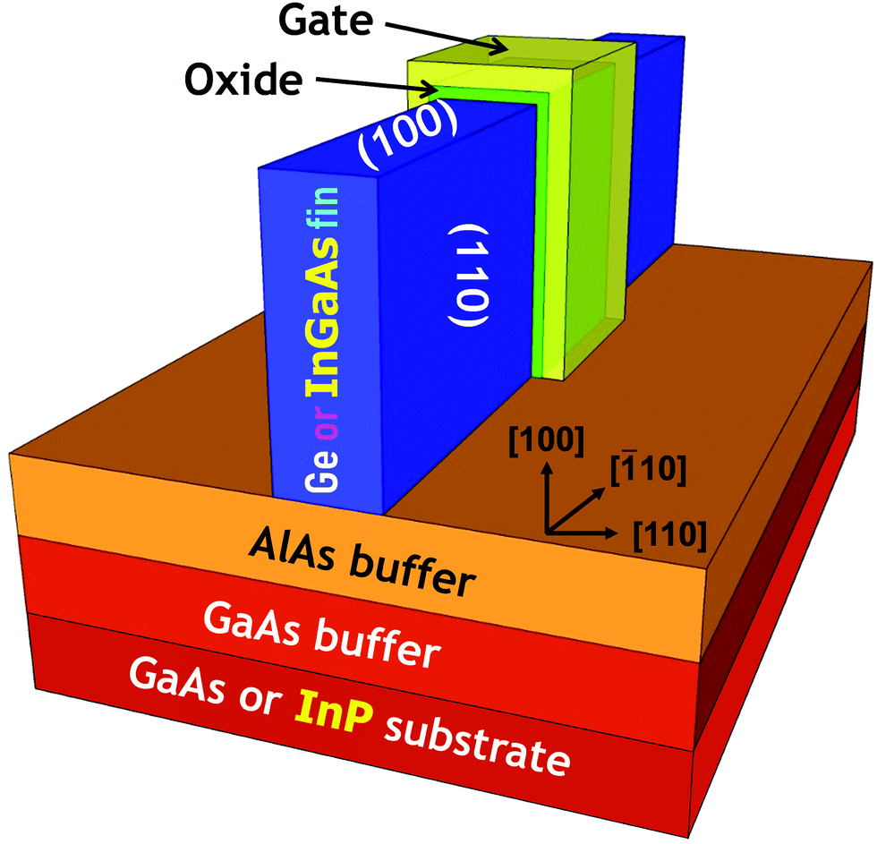 | ||
| Fig. 1 Schematic representation of the orientation-specific lattice matched Ge on AlAs/GaAs and InGaAs/InP fin transistor architecture, where (100) and (110) surfaces are of technological importance for ultra-low power electronic devices. Here, the lattice matched epitaxial Ge and InGaAs layers were realized on GaAs substrate with an intermediate AlAs buffer layer and InP substrate, respectively. The respective substrate orientations were used for synthesizing orientation-specific Ge or InGaAs layers.16,33 | ||
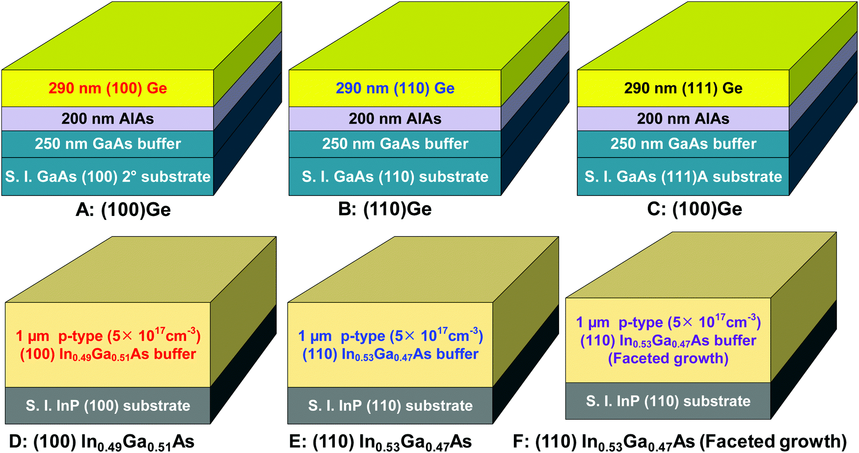 | ||
| Fig. 2 Schematic representation of the orientation-specific lattice matched (a) (100)Ge on semi-insulating (S. I.) (100)GaAs, (b) (110)Ge on (110)GaAs, and (c) (111)Ge on (111)A GaAs substrate, respectively. For epitaxial Ge heterostructure, 200 nm of the AlAs intermediate buffer layer was used, which served as a barrier layer and also provided a large band offset between Ge and AlAs than Ge on GaAs.13 Here all the Ge epitaxial layers are n-type (unintentionally doped) and the doping was ∼2 × 1018 cm−3. (d)–(f) shows the beryllium (Be)-doped p-type (5 × 1017 cm−3) 1 μm thick (100)InGaAs, (110)InGaAs and (110)InGaAs (faceted growth) on InP substrate, respectively. | ||
A Probing facets in (110) InGaAs/InP heterostructures
Atomic force microscopy analysis was performed from the surface of orientation-specific InGaAs/InP heterostructures. Fig. 3 shows the 20 μm × 20 μm AFM micrographs (3D view) from the surface of the InGaAs layers grown on (100) and (110) InP substrates, where one can observe the faceted growth of InGaAs layers on (110)InP substrates (see samples E and F). It has been reported that the epitaxial (110)InGaAs layer has a tendency to exhibit a crystallographically faceted surface during growth.7,39–41 The growth temperature, growth rate, and group V/III ratio are the key growth parameters in order to achieve smooth surface morphologies.7 The root mean square (rms) surface roughness of ∼0.28 nm, ∼7.5 nm and ∼20 nm over the 20 × 20 μm2 scan area from the surface of (100) In0.49Ga0.51As (Sample D), (110) In0.53Ga0.47As (Sample E), and (110) In0.53Ga0.47As (Sample F), respectively, were measured. The higher surface roughness and different surface facets were observed for the (110) In0.53Ga0.47As (Sample F) than (100) In0.49Ga0.51As (Sample D), which affected the carrier lifetime, as discussed below.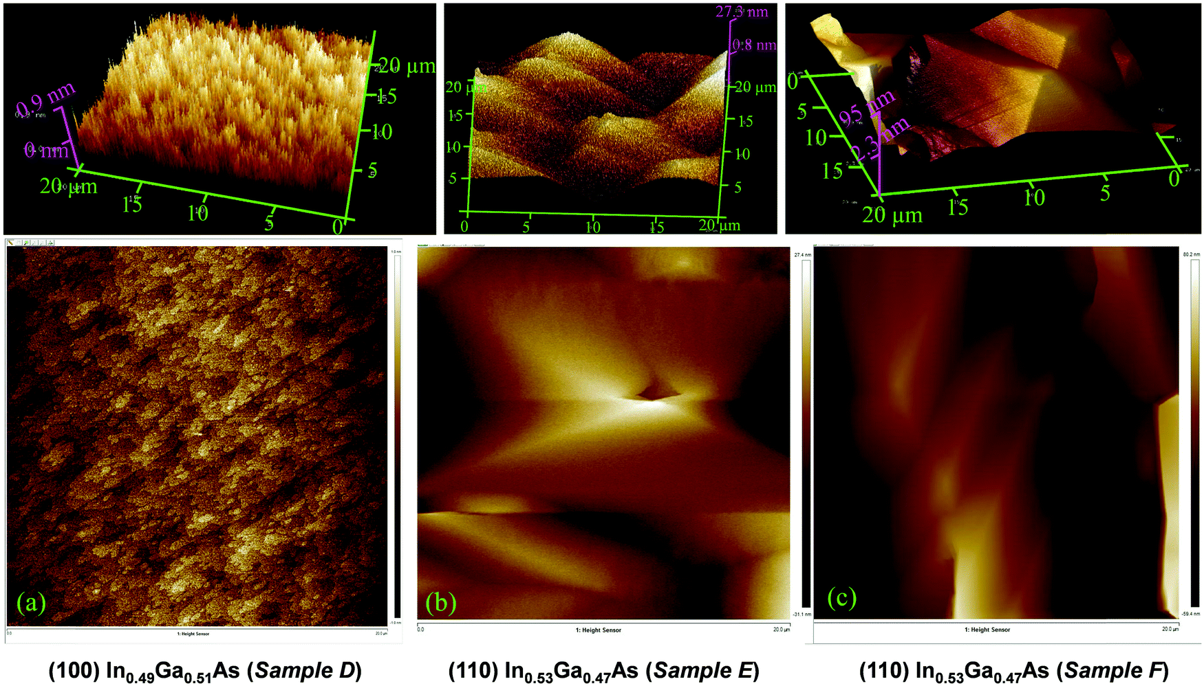 | ||
| Fig. 3 The 3D (top-view) and 2D (bottom) AFM micrographs from the surface of 1 μm thick (a) In0.49Ga0.51As (Sample D), (b) In0.53Ga0.47As (Sample E), and (c) In0.53Ga0.47As (Sample F) layers, demonstrating root mean square (rms) roughness of ∼0.28 nm (Sample D), ∼7.5 nm (Sample E), ∼20 nm (Sample F) over the 20 × 20 μm2 scan area. A uniformly smooth surface morphology was observed from (100) In0.49Ga0.51As than from In0.49Ga0.51As layers that were grown on (110)InP substrates. | ||
B Carrier lifetimes in the oriented Ge/AlAs heterostructures
Carrier lifetimes from lattice-matched Ge/AlAs heterostructures with three different surface orientations were determined by a non-contact μ-PCD method. As discussed above, the carrier lifetime has a strong orientation dependence on elementary (Si, Ge) and binary (GaAs, GaN) semiconductors,23,26,28,37 as well as a few oxide materials.31,32 Over the decades, different measurement techniques, such as temperature-dependent photoluminescence, microwave reflection and transmission probing, and non-contact PCD, have been developed42–54 for the determination of the carrier lifetime. In this work, the carrier recombination properties in the oriented Ge/AlAs heterostructures were investigated at room temperature using the μ-PCD method. The carrier recombination properties from each Ge/AlAs heterostructure were studied as a function of surface orientation (seeFig. 2). An excitation wavelength of 1500 nm (0.826 eV) was used during the measurement, and the carrier lifetimes were quantified by fitting the decay curve after a short ∼3 ns optical excitation pulse ended. To gain further insights into the carrier recombination properties, an excitation wavelength of 1800 nm (0.688 eV) was used, especially for the (111)Ge/AlAs heterostructure since it has the lowest amount of surface states, as reported by Hsieh et al.24 as well as lowest carrier lifetime as compared with the result obtained from the 1500 nm excitation. Fig. 4 shows the μ-PCD signal obtained from each (100)Ge/AlAs, (110)Ge/AlAs, and (111)Ge/AlAs heterostructures measured at an excitation wavelength of 1500 nm. The penetration depth at this excitation wavelength is much larger than the thickness of each heterostructure since the absorption coefficient of Ge at this excitation is ∼4 × 103 cm−1. Fig. 4a shows the μ-PCD signal versus the time recorded from each Ge/AlAs heterostructure. One can find from this figure that there are two-time scale windows, highlighted by the two shaded areas, I and II for carrier recombination. The excess photogenerated carriers’ recombination at the surface is responsible for the initial decay process (region I). In this time window, photogenerated carriers could start to diffuse into the bulk, but the rate of diffusion would be significantly smaller due to the surface recombination. This process could enhance samples with higher surface roughness than those with smooth surfaces. One can find that the μ-PCD signal from the region I is almost identical to these three oriented Ge/AlAs heterostructures, which is indicative of similar surface roughness and similar surface trap density. If the surface trap density is higher in (111)Ge/AlAs heterostructure than in other orientations, one could expect a lower μ-PCD signal. The small increase in μ-PCD signal from (111)Ge/AlAs heterostructure in the region I supports our conclusion of a similar or lower surface trap density.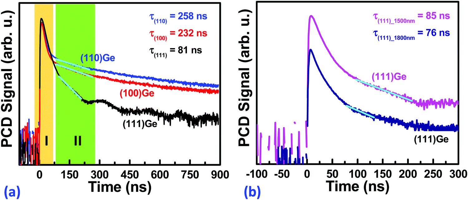 | ||
| Fig. 4 (a) μ-PCD data at 300 K obtained from the crystallographically oriented epitaxial (100)Ge, (110)Ge, (111)Ge layer grown on respective GaAs substrates with intermediate AlAs buffer layer, wherein the excitation at a 1500 nm wavelength (0.826 eV) was applied from the front side of each heterostructure and the laser power was 20 mW. The figure also shows the fits to the data (Cyan) for each PCD signal, wherein the effective carrier lifetime was determined (Region II) for each sample studied here. The initial PCD signal decreases sharply from 0 ns to 75 ns after excitation (Region I). (b) μ-PCD signal from the (111)Ge at two different excitation wavelengths: 1500 nm and 1800 nm (0.688 eV). The measured data has been offset for clarity. The measured lifetime data from the (111)Ge heterostructure is lower than from either (100)Ge or (110)Ge heterostructure. | ||
In the time-scale window II, these excess carriers would have diffused into the bulk of each Ge/AlAs heterostructure, and the carrier lifetime can be extracted. These carrier lifetimes are predominantly the bulk lifetime of carriers via Shockley–Read–Hall (SRH) recombination, which is related to carrier trapping impurities or defects. By fitting the measured μ-PCD data (VPCD) to 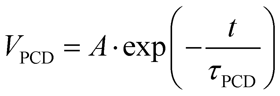 , shown in the second shaded area (II) for each heterostructure (Cyan color), the μ-PCD lifetimes (τPCD) were determined, t is the time, where A is a pre-exponential constant. Higher carrier lifetimes of 232 ns and 258 ns, respectively, were obtained from (100)Ge/AlAs and (110)Ge/As heterostructure. On the other hand, a lower carrier lifetime of 81 ns was extracted from the (111)Ge/AlAs heterostructure, which is ∼3 times lower than the carrier lifetime from either (100)Ge or (110)Ge heterostructure, which could be due to the higher bulk trap state density or high electrical conductivity. In addition, the μ-PCD decay signal is oscillating starting from region II. The oscillations are apparent since this is low signal amplitude down a couple of orders of magnitude from the initial signal and after most of the decay has already occurred. This oscillation could be an artifact of electronics and cables and could be small amounts of electrical signal that get reflected at impedance mismatches when connecting electronic devices, such as amplifiers and rectification diodes. Irrespective of the oscillation, the carrier lifetime was lower in (111)Ge/AlAs heterostructure compared to other-oriented Ge layers.
The carrier lifetime was further evaluated from the (111)Ge/AlAs heterostructure at 1800 nm (0.688 eV) and compared with 1500 nm (0.826 eV) excitation wavelength. The excitation wavelength of 1500 nm was selected for both L- and Γ-valley carrier absorption, and the 1800 nm was used only for L-valley carrier absorption. It was observed that the separation between the L- and Γ-valleys is ∼ 120 meV. Fig. 4b shows the μ-PCD signal as a function of time from the (111)Ge/AlAs heterostructure measured at two excitation wavelengths: 1500 nm and 1800 nm. The fitting was performed for these two μ-PCD signals and the carrier lifetime from each excitation wavelength is indicated in this figure. Table 1 shows the measured orientation-specific carrier lifetime of Ge/AlAs heterostructures as determined using the μ-PCD method. The linear regression analysis was performed for selecting the fitting ranges to extract the carrier lifetime, where the R2 number in Table 1 defines how close the experimental data range was fitted by a regression line (Cyan color). A higher R2 number indicates a better fit. One can find from this figure that the carrier lifetime for (111)Ge/(111)AlAs is near 80 ns at both excitation wavelengths, which is 3 times lower than the carrier lifetime from either (100)Ge/AlAs or (110)Ge/AlAs heterostructures. The higher minority carrier lifetimes obtained from (100)Ge/AlAs and (110)Ge/AlAs are beneficial for Ge-based nanoscale fin transistors, as shown in Fig. 1.
C Carrier lifetimes in oriented InGaAs/InP heterostructures
The μ-PCD signal data as a function of time from oriented InGaAs/InP heterostructures at room temperature are shown in Fig. 5a and b. The excitation wavelength of 1500 nm (0.826 eV) was used for this measurement and the excitation laser power was 1000 times lower on (100)InGaAs surface than on (110)InGaAs surfaces to ensure low-level injection on (100)InGaAs surface. The fitted data (cyan color) to the measured PCD signal yielded carrier lifetimes of 125 μs (Fig. 5b) and 10 ns (Fig. 5a) from (100)InGaAs/InP and (110)InGaAs/InP heterostructure, respectively. The μ-PCD signal from both the (110)InGaAs epitaxial layers (E and F) exhibited a carrier lifetime of 10 ns. The lower lifetime of 10 ns from (110)InGaAs epitaxial layer is due to the facet-dependent growth on the (110)InP substrate, as shown in Fig. 3. The facet-dependent growth was observed earlier from the (110)InGaAs surface,7,33,39–41 and now displayed a lower carrier lifetime. One can find from Fig. 5a that the carrier recombination is solely dominant from the surface before the signal is diffused into the bulk of each (110)InGaAs layer. One can passivate these (110)InGaAs surfaces via atomic layer deposited dielectrics, such as Al2O3, to reduce carrier recombination at the surface and allow carriers to diffuse into the bulk of the material and hence increase the carrier lifetime.46,51,55–59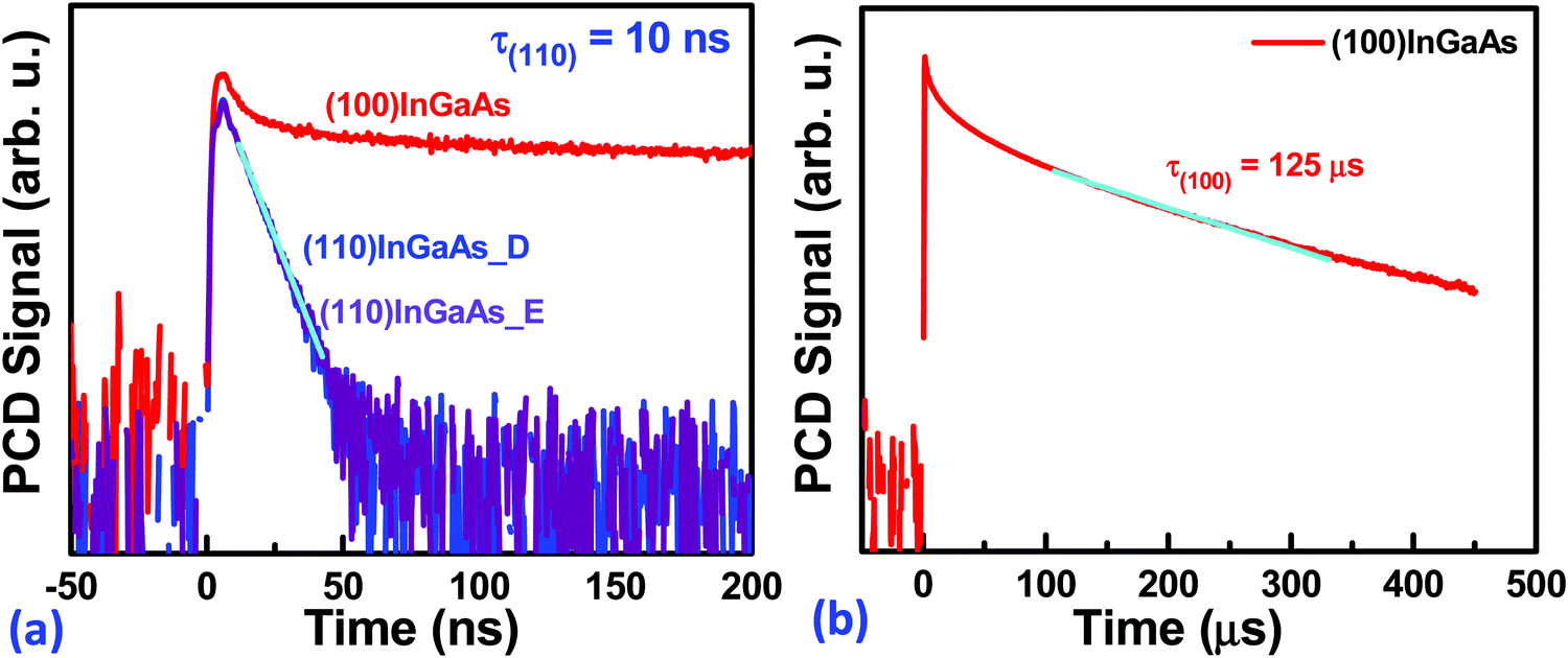 | ||
| Fig. 5 (a) μ-PCD data at 300 K obtained from the oriented (100)In0.49Ga0.51As, (110)In0.53Ga0.47As_D and (110)In0.53Ga0.47As_E (faceted)/InP heterostructures with same 1.0 μm thicknesses, wherein the excitation at a 1500 nm wavelength was applied from the front side of each heterostructure. The excitation laser power on the (100)InGaAs was 1000× lower than (110)InGaAs layers. The figure also shows the fits to the data (Cyan) for each μ-PCD signal, where the effective carrier lifetime was determined for each sample. (b) The carrier lifetime of 125 μs was determined from (100)In0.49Ga0.51As/InP heterostructure, and the carrier lifetime of 10 ns was extracted from both (110)In0.53Ga0.47As/InP heterostructures. | ||
Conclusions
The orientation-specific carrier lifetimes in epitaxial Ge/AlAs and InGaAs/InP heterostructures were evaluated using the contactless microwave photoconductivity decay technique using a 1500 nm excitation source incident on the front (top) side of each heterostructure. A vacuum-interconnected dual-chamber, solid source molecular beam epitaxy deposition system with added in situ surface analysis capability was used for oriented Ge/AlAs and InGaAs/InP materials synthesis. High carrier lifetimes of more than 200 ns were measured at room temperature for the (100)Ge/AlAs and (110)Ge/AlAs heterostructures, and 3 times lower carrier lifetime from (111)Ge/AlAs heterostructure than (100)Ge and (110)Ge. The carrier lifetimes of 125 μs and 10 ns from the (100)InGaAs/InP and the (110)InGaAs/InP heterostructure, respectively, were determined. A reduction of carrier lifetime in (111)Ge and (110)InGaAs layers could be related to higher bulk trap state density or high electrical conductivity, and facet-dependent growth of these layers, respectively. A surface passivating layer is essential for these oriented epitaxial layers to improve the carrier lifetime, which has been reported by several researchers. The higher carrier lifetimes from (100)Ge and (110)Ge demonstrated the suitability of the Ge fin transistor and optoelectronic devices based on the (100)InGaAs layer.Author contributions
Mantu Hudait: conceptualization, resources, supervision, project administration, funding acquisition, methodology, data curation, investigation, visualization, writing the original draft, reviewing and editing; Steven Johnston: resources, lifetime data collection, investigation, writing – review and editing.Conflicts of interest
There are no conflicts to declare.Acknowledgements
M. K. H. acknowledges past partial support from the NSF under grant number ECCS-1507950, a US-Ireland joint R&D program for germanium epilayer growth on III–V buffer for tunnel transistor. The authors also acknowledge Virginia Tech Nanofabrication facilities for assistance during materials analysis. The authors also like to thank M. Clavel for assisting materials growth and surface morphology, and S. Karthikeyan for technical discussions.References
- K. J. Kuhn, Considerations for Ultimate CMOS Scaling, IEEE Trans. Electron Devices, 2012, 59, 1813–1828 CAS.
- A. Toriumi and T. Nishimura, Germanium CMOS potential from material and process perspectives: Be more positive about germanium, Jpn. J. Appl. Phys., 2018, 57, 010101 CrossRef.
- K. Liu, E. Ko, S. Kim, J. Park, C. S. Hwang and J.-H. Choi, Orientation-dependent structural and electronic properties of Ge/a-GeO2 interfaces: first-principles study, J. Phys. D: Appl. Phys., 2019, 52, 155101 CrossRef.
- P. D. Nguyen, M. B. Clavel, A. Ghosh and M. K. Hudait, Metal work function engineering on epitaxial (100)Ge and (110)Ge metal-oxide-semiconductor devices, Microelectron. Eng., 2018, 199, 80–86 CrossRef CAS.
- P. D. Nguyen, M. B. Clavel, J.-S. Liu and M. K. Hudait, Investigating FinFET Sidewall Passivation Using Epitaxial (100)Ge and (110)Ge Metal–Oxide–Semiconductor Devices on AlAs/GaAs, IEEE Trans. Electron Devices, 2017, 64, 4457–4465 CAS.
- T. Kent, et al., The Influence of Surface Preparation on Low Temperature HfO2 ALD on InGaAs (001) and (110) Surfaces, J. Chem. Phys., 2015, 143, 164711-1-8 CrossRef PubMed.
- C. D. Yerino, B. Liang, D. L. Huffaker, P. J. Simmonds and M. L. Lee, Molecular Beam Epitaxy of Lattice-Matched InAlAs and InGaAs Layers on InP (111)A, (111)B and (110), J. Vac. Sci. Technol., B: Nanotechnol. Microelectron.: Mater., Process., Meas., Phenom., 2017, 35, 010801-1-31 Search PubMed.
- N. Waldron et al. , An InGaAs/InP quantum well finfet using the replacement fin process integrated in an RMG flow on 300 mm Si substrates, 2014 Symposium on VLSI Technology: Digest of Technical Papers, 2014, pp. 1–2.
- M. Yokoyama, R. Suzuki, N. Taoka, M. Takenaka and S. Takagi, Impact of Surface Orientation on (100), (111)A, and (111)B InGaAs Surfaces with In Content of 0.53 and 0.70 and on Their Al2O3/InGaAs Metal-Oxide-Semiconductor Interface Properties, Appl. Phys. Lett., 2016, 109, 182111-1-4 Search PubMed.
- M. Radosavljevic, et al., Electrostatics Improvement in 3-D Tri-gate Over Ultra-Thin Body Planar InGaAs Quantum Well Field Effect Transistors with High-K Gate Dielectric and Scaled Gate-to-Drain/Gate-to-Source Separation, IEDM Tech. Dig., 2011, 765–768 CAS.
- S. Krivec, M. Poljak and T. Suligoj, Electron Mobility in Ultra-thin InGaAs Channels: Impact of Surface Orientation and Different Gate Oxide Materials, Solid-State Electron., 2016, 115, 109–119 CrossRef CAS.
- C. Convertino, C. Zota, H. Schmid, D. Caimi, M. Sousa, K. Moselund and L. Czornomaz, InGaAs FinFETs Directly Integrated on Silicon by Selective Growth in Oxide Cavities, Materials, 2019, 12, 87 CrossRef CAS PubMed.
- M. K. Hudait, M. Clavel, P. Goley, N. Jain and Y. Zhu, Heterogeneous Integration of Epitaxial Ge on Si using AlAs/GaAs Buffer Architecture: Suitability for Low-power Fin Field-Effect Transistors, Sci. Rep., 2014, 4, 6964–6969 CrossRef CAS PubMed.
- R. Zhang, X. Yu, M. Takenaka and S. Takagi, Impact of Channel Orientation on Electrical Properties of Ge p- and n-MOSFETs With 1-nm EOT Al2O3/GeOx/Ge Gate-Stacks Fabricated by Plasma Post oxidation, IEEE Trans. Electron Devices, 2014, 61, 3668–3675 CAS.
- P. D. Nguyen, M. Clavel, P. Goley, J.-S. Liu, N. Allen, L. J. Guido and M. K. Hudait, Heteroepitaxial Ge MOS Devices on Si Using Composite AlAs/GaAs Buffer, IEEE J. Electron Devices Soc., 2015, 3, 341–348 CAS.
- M. K. Hudait, Y. Zhu, N. Jain and J. L. Hunter, Jr., Structural, Morphological, and Band Alignment Properties of GaAs/Ge/GaAs Heterostructures on (100), (110) and (111)A GaAs Substrates, J. Vac. Sci. Technol., B: Nanotechnol. Microelectron.: Mater., Process., Meas., Phenom., 2013, 31, 011206-1-14 Search PubMed.
- K. H. Lee, et al., Hetero-epitaxy of high quality germanium film on silicon substrate for optoelectronic integrated circuit applications, J. Mater. Res., 2017, 32, 4025–4040 CrossRef CAS.
- P. S. Goley and M. K. Hudait, Germanium based field-effect transistors: challenges and opportunities, Materials, 2014, 7, 2301–2339 CrossRef CAS PubMed.
- F. Sansoz, Surface Faceting Dependence of Thermal Transport in Silicon Nanowires, Nano Lett., 2011, 11, 5378–5382 CrossRef CAS PubMed.
- W. J.-H. Berghuis, J. Melskens, B. Macco, R. J. Theeuwes, M. A. Verheijen and W. M. Kessels, Surface passivation of germanium by atomic layer deposited Al2O3 nanolayers, J. Mater. Res., 2021, 36, 571–581 CrossRef CAS.
- S. Bai, L. Wang, Z. Li and Y. Xiong, Facet-Engineered Surface and Interface Design of Photocatalytic Materials, Adv. Sci., 2017, 4, 1600216 CrossRef PubMed.
- M. H. Huang, G. Naresh and H.-S. Chen, Facet-Dependent Electrical, Photocatalytic, and Optical Properties of Semiconductor Crystals and Their Implications for Applications, ACS Appl. Mater. Interfaces, 2018, 10, 4–15 CrossRef CAS PubMed.
- C.-S. Tan, Y. Zhao, R.-H. Guo, W.-T. Chuang, L.-J. Chen and M. H. Huang, Facet-Dependent Surface Trap States and Carrier Lifetimes of Silicon, Nano Lett., 2020, 20, 1952–1958 CrossRef CAS PubMed.
- C.-S. Tan, M.-Y. Lu, W.-H. Peng, L.-J. Chen and M. H. Huang, Germanium Possessing Facet-Specific Trap States and Carrier Lifetimes, J. Phys. Chem. C, 2020, 124, 13304–13309 CrossRef CAS.
- C.-S. Tan and M. H. Huang, Density Functional Theory Calculations Revealing Metal-like Band Structures for Ultrathin Germanium (111) and (211) Surface Layers, Chem. – Asian J., 2018, 13, 1972–1976 CrossRef CAS PubMed.
- C. S. Tan, Density Functional Theory Study of Metallic Silicon (111) Plane Structures, ACS Omega, 2022, 7(6), 5385–5392 CrossRef CAS PubMed.
- P.-L. Hsieh, A.-T. Lee, L.-J. Chen and M. H. Huang, Germanium Wafers Possessing Facet-Dependent Electrical Conductivity Properties, Angew. Chem., 2018, 130, 16394–16397 CrossRef.
- C.-S. Tan, L.-J. Chen and M. H. Huang, Large Facet-Specific Built-in Potential Differences Affecting Trap State Densities and Carrier Lifetimes of GaAs Wafers, J. Phys. Chem. C, 2020, 124, 21577–21582 CrossRef CAS.
- M. H. Huang, Semiconductor nanocrystals possessing broadly size- and facet-dependent optical properties, J. Chin. Chem. Soc., 2021, 68, 45–50 CrossRef CAS.
- M. H. Huang, Facet-dependent optical properties of semiconductor nanocrystals, Small, 2019, 15, 1804726 CrossRef PubMed.
- M. Kato, K. Kohama, Y. Ichikawa and M. Ichim, Carrier lifetime measurements on various crystal faces of rutile TiO2 single crystals, Mater. Lett., 2015, 190, 397–399 CrossRef.
- M. Kato, T. Ozawa and Y. Ichikawa, Carrier recombination in SrTiO3 single crystals: impacts of crystal faces and Nb doping, J. Phys. D: Appl. Phys., 2021, 54, 345106 CrossRef CAS.
- M. K. Hudait, M. B. Clavel, J.-S. Liu and S. Bhattacharya, In Situ SiO2 Passivation of Epitaxial (100) and (110)InGaAs by Exploiting TaSiOx Atomic Layer Deposition Process, ACS Omega, 2018, 3, 14567–14574 CrossRef CAS PubMed.
- D. B. Migas, V. E. Borisenko, Rusli and C. Soci, Revising morphology of 〈111〉-oriented silicon and germanium nanowires, Nano Convergence, 2015, 2, 16, DOI:10.1186/s40580-015-0044-8.
- J. G. Fiorenza, et al., A. Aspect Ratio Trapping: A Unique Technology for Integrating Ge and III-Vs with Silicon CMOS, ECS Trans., 2010, 33, 963–976 CrossRef CAS.
- M. N. Mankin, et al., Facet-Selective Epitaxy of Compound Semiconductors on Faceted Silicon Nanowires, Nano Lett., 2015, 15, 4776–4782 CrossRef CAS PubMed.
- P.-L. Hsieh, G. Kumar, Y.-Y. Wang, Y.-J. Lu, L.-J. Chen and M. H. Huang, Facet-dependent electrical conductivity properties of GaN wafers, J. Mater. Chem. C, 2021, 9, 15354–15358 RSC.
- K. L. Chopra and S. R. Das, Thin Film Solar Cells, Springer, New York, 1983, p. 146 Search PubMed.
- R. Vardya, S. Mahajan and R. Bhat, Microstructural Characteristics of (110) InGaAs Layers Grown by OMVPE, Mater. Sci. Eng., B, 1995, 33, 148–155 CrossRef.
- O. Ueda, Y. Nakata, T. Nakamura and T. Fuji, TEM Investigation of CuAu-I Type Ordered Structures in MBE-Grown InGaAs Crystals on (110) InP Substrates, J. Cryst. Growth, 1991, 115, 375–380 CrossRef CAS.
- R. Bhat, M. A. Koza, D. M. Hwang, M. J.-S. P. Brasil, R. E. Nahory and K. Oe, OMCVD Growth of InP, InGaAs, and InGaAsP on (110) InP Substrates, J. Cryst. Growth, 1992, 124, 311–317 CrossRef CAS.
- S. Johnston, K. Zaunbrecher, R. Ahrenkiel, D. Kuciauskas, D. Albin and W. Metzger, Simultaneous Measurement of Minority-Carrier Lifetime in Single-Crystal CdTe Using Three Transient Decay Techniques, IEEE J. Photovoltaics, 2014, 4, 1295 Search PubMed.
- E. Gaubas and J. Vanhellemont, Dependence of carrier lifetime in germanium on resistivity and carrier injection level, Appl. Phys. Lett., 2006, 89, 142106 CrossRef.
- P.-C. Hsu, et al., The impact of extended defects on the generation and recombination lifetime in n type In0.53Ga0.47As, J. Phys. D: Appl. Phys., 2019, 52, 485102 CrossRef CAS.
- B. Sermage, J. L. Benchimol and G. M. Cohen, Carrier lifetime in p-doped InGaAs and InGaAsP, Conference Proceedings. 1998 International Conference on Indium Phosphide and Related Materials (Cat. No. 98CH36129), 1998, pp. 758–760.
- H. J. Joyce, et al., Ultralow surface recombination velocity in InP nanowires probed by terahertz spectroscopy, Nano Lett., 2012, 12, 5325–5330 CrossRef CAS PubMed.
- C. H. Henry, R. A. Logan, F. R. Merritt and C. G. Bethea, Radiative and nonradiative lifetimes in n-type and p-type 1.6 μm InGaAs, Electron. Lett., 1984, 20, 358–359 CrossRef CAS.
- R. K. Ahrenkiel, R. Ellingson, S. Johnston and M. Wanlass, Recombination lifetime of In0.53Ga0.47As as a function of doping density, Appl. Phys. Lett., 1998, 72, 3470–3472 CrossRef CAS.
- M. Gallant and A. Zemel, Long minority hole diffusion length and evidence for bulk radiative recombination limited lifetime in InP/InGaAs/InP double heterostructures, Appl. Phys. Lett., 1988, 52, 1686–1688 CrossRef CAS.
- E. Malysheva, D. Pellegrino, A. Fiore, K. Williams and V. D. Calzadilla, Impact of High Temperature Post-Treatment on Photoluminescence Performance of Passivated InP/In0.53Ga0.47As/InP Nanopillars, 2021 Conference on Lasers and Electro-Optics Europe & European Quantum Electronics Conference (CLEO/Europe-EQEC), 2021, pp. 1–1.
- A. Higuera-Rodriguez, et al., Ultralow surface recombination velocity in passivated InGaAs/InP Nanopillars, Nano Lett., 2017, 17, 2627 CrossRef CAS PubMed.
- E. Cornagliotti, G. Agostinelli, J. Van Der Heide, N. E. Posthuma, G. Beaucarne and J. Poortmans, Extension of QSSPC lifetime measurement to germanium samples, In Conference Record of the 2006 IEEE 4th World Conference on Photovoltaic Energy Conversion (IEEE, 2006), pp. 1869–1871.
- S. Dev, et al., Measurement of carrier lifetime in micron-scaled materials using resonant microwave circuits, Nat. Commun., 2019, 10, 1625 CrossRef PubMed.
- E. Gaubas and J. Vanhellemont, Comparative Study of Carrier Lifetime Dependence on Dopant Concentration in Silicon and Germanium, J. Electrochem. Soc., 2007, 154, H231–H238 CrossRef CAS.
- H. Liu, G. Han, Y. Liu, X. Tang, J. Yang and Y. Hao, High mobility Ge pMOSFETs with amorphous Si passivation: impact of surface orientation, Nano Res. Lett., 2019, 14, 15 CrossRef PubMed.
- B. Hoex, S. B.-S. Heil, E. Langereis, M. C.-M. Van De Sanden and W. M.-M. Kessels, Ultralow surface recombination of c-Si substrates passivated by plasma-assisted atomic layer deposited Al2O3, Appl. Phys. Lett., 2006, 89, 042112 CrossRef.
- C. C. Chang, et al., Electrical and optical characterization of surface passivation in GaAs nanowires, Nano Lett., 2012, 12, 4484–4489 CrossRef CAS PubMed.
- Q. Xie, et al., Germanium surface passivation and atomic layer deposition of high-k dielectrics--a tutorial review on Ge-based MOS capacitors, Semicond. Sci. Technol., 2012, 27, 1–12 Search PubMed.
- T. Sasada, Y. Nakakita, M. Takenaka and S. Takagi, Surface orientation dependence of interface properties of GeO2/Ge metal-oxide-semiconductor structures fabricated by thermal oxidation, J. Appl. Phys., 2009, 106, 073716 CrossRef.
| This journal is © The Royal Society of Chemistry 2022 |