
 Open Access Article
 This Open Access Article is licensed under a
 Creative Commons Attribution 3.0 Unported Licence
Storing electronic information on semi-metal nanoparticles
Febin
Paul
,
Krishna
Nama Manjunatha
 and
Shashi
Paul
*
and
Shashi
Paul
*
Emerging Technologies Research Centre, De Montfort University, The Gateway, Leicester, LE18BH, UK. E-mail: spaul@dmu.ac.uk
First published on 11th May 2022
Abstract
This paper presents the use of selenium nanoparticles for applications in information storage in two-terminal electronic memory devices. Selenium is a semi-metal with interesting electronic and optical properties that have seldom been studied in terms of electronic memory. In this study, selenium nanoparticles have been demonstrated as an embedded charge storage layer between the silicon oxide tunnel layer and the silicon nitride blocking layer. The electrical characterization demonstrates clear evidence that charge storage occurs, and that the presence of nanoparticles is indispensable. AFM images show that selenium nanoparticles are almost uniformly distributed on a silicon substrate having a thin silicon dioxide tunnelling layer, and the electrical retention measurement shows potential for long-term data storage.
Introduction
The past few decades have seen a steady rise in the area of emerging non-volatile electronic memory devices. A surge in popularity in this field has led to several works being published about new materials such as metal-oxides,1,2 perovskites,3 chalcogenides,4 and polymer nanocomposites.5–8 Several studies have introduced newer device structures1,9–12 and even newer techniques of device fabrications.12–16 However, the translation of much of the innovative novel work that has been done in the past into the progress in the field has been slow due to issues related to device-to-device variation and lack of repeatability.17 Several research groups have worked on the same system and similar device structures but the results in regard to the role of nanoparticles in conduction switching from these studies have been quite unclear.18–20 Several models, such as electric field induced charge transfer, polymer doping, and Simon–Verderber mechanism, have been put forward in the past to explain the device operation; while these succeed in explaining certain facets of the device behavior, several other aspects remain unclear,21–23 for example, questions such as why device switching affects the repeatability as the ON/OFF ratio increases and the role of the nanoparticles in the process of conduction switching. Since these questions have been discussed in detail in our previous work,24 this work is limited in its full discussion.The focus of this study is to further examine and understand the charge storage mechanism by fabricating a selenium nanoparticle-based memory device. Selenium is an interesting material due to its photoelectric conductivity and has the ability to change its resistance on exposure to light.24 Selenium has been used in various applications due to its enhanced photoelectric response. Recently, 2D nanoflakes of selenium were investigated for applications in self-powered photodetectors25 and ultrafast photonic applications.26 Some materials such as tellurene have poor photoelectric response and are improved by blending with selenium for applications in photodetectors.27 Bulk selenium has been used for quite a while in photocopiers as a charge-trap layer. Due to the enhanced photoresponse of selenium, its use in charge storage devices such as memory devices will allow the development of photonic memory devices, where the data is light written and erased, which is ultrafast and also energy efficient. The photosensitive resistance of selenium is of interest to trap charges and uses an electric field for printing application. This has been widely attributed to the differences in hole and electron mobility in the material.28,29 This study focuses on a similar principle, albeit the application of long-term storage of charges. It can be safely argued that the confined nanostructures of selenium would have enhanced charge trapping ability compared to bulk selenium.
However, most importantly, the work function of selenium makes it particularly attractive for non-volatile electronic memory applications. The delicate balance of the work function plays a significant role in the effective storage of information; a higher work function leads to a reduction in the barrier potential, which favors low voltage programming and additionally offers a large barrier that prevents the loss of data.30 This factor makes the use of gold (Au) and platinum (Pt) very desirable, but a careful study of selenium unravels the benefits over the former elements in this regard and may eliminate the use of expensive metals. Selenium has a work of function of 5.1 eV,31 which is greater than or closer to metals such as gold (5.1 eV), nickel (4.96 eV), silver (4.33 eV), or aluminium (4.24 eV).30 Apart from the work function, selenium is not easily oxidized and can be deposited using simple thin film deposition technique such as thermal evaporation.32
Experimental details
Device structure
The device structure constitutes of a modified three-layer (3L) structure, wherein a semi-metal nanoparticle layer would be embedded within an insulator/semiconductor matrix. In this study, selenium nanoparticles have been laid between two dielectric layers, namely, silicon dioxide (SiO2) and silicon nitride (SiNx) (refer Fig. 1). The silicon nitride layer is intended to be thick so that charge leakage would be highly unlikely; therefore, it is labelled as the blocking layer. Silicon oxide, on the other hand, is known as the tunnelling layer and, as the name suggests, is intended for the purpose of charge injection in the form of tunnelled charges when an external voltage is applied.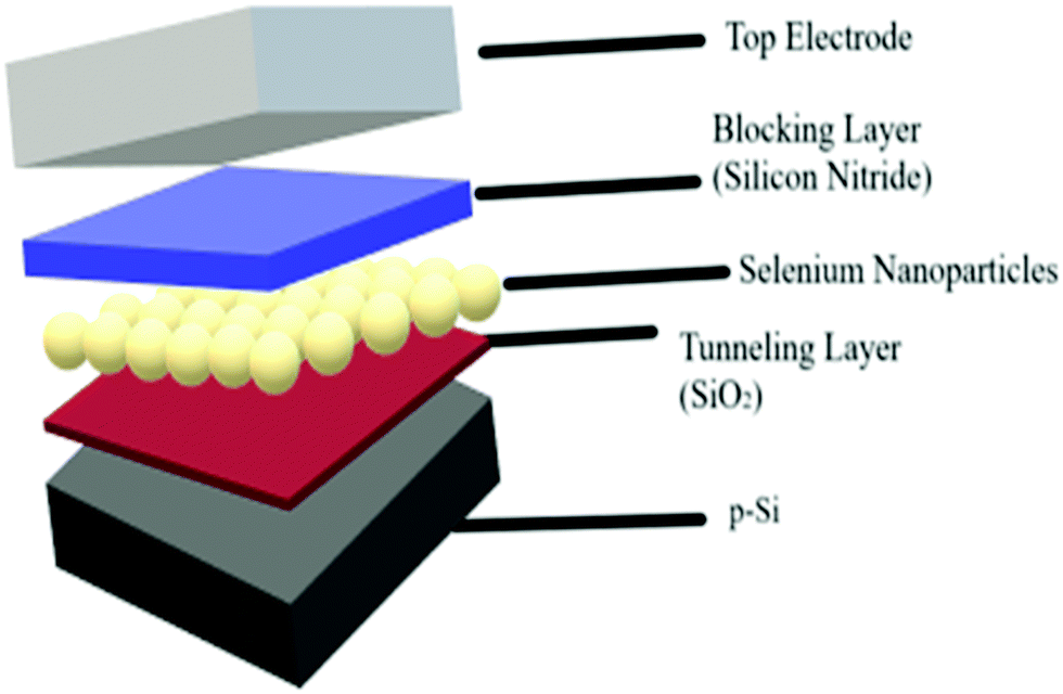 | ||
| Fig. 1 Metal-Insulator-Semiconductor (MIS) device structure with Se-NPs as a charge storage medium. Tunnelling layer is SiO2 (2 nm), blocking Layer is SiNx (100 nm), charge storage layer is composed of selenium nanoparticles sandwiched between aforementioned dielectric layers deposited on boron-doped P-Silicon wafer (1–10 Ohm per cm, 500 μm thickness). Top and bottom ohmic electrodes are made of aluminium (Al). | ||
Device fabrication
The charge storage material used in this work is selenium nanoparticles (SeNPs) deposited by thermal evaporation of selenium (purity ≥ 99.999%) using a thermal evaporator (Edwards Auto-306, Se is purchased from Sigma-Aldrich). Evaporation was performed at 0.1 nm s−1 until a thickness of 5 nm was achieved. It is worth mentioning that the thickness reported here reflects the mass thickness of Se, as determined by the quartz crystal microbalance attached to a film thickness monitor. This does not reflect the nanoparticle size of selenium. The radius of nanoparticles is about 100 nm ± 18 nm, which as is also seen in the AFM images included later in this manuscript. The metal-insulator-semiconductor (MIS) devices were fabricated on boron-doped p-Si wafers (500 μm, 1–20 Ohm per cm) with Al back ohmic contact. The sandwich structure above the silicon surface with Se–NPs (charge storage device) and without Se–NPs (reference device) was achieved with two dielectric insulator thin films, namely, silicon oxide (SiO2) and silicon nitride (SiNx). The thickness of the SiO2 layer was 2 nm, which is used in this work as the tunnelling layer to allow the tunnelling of charge carriers, and the thickness of the SiNx layer was 100 nm, which is used in this work as a charge blocking layer. The details of the deposition process conditions of each layer are summarized in Table 1. Device structures are as follows: reference device Al/p-Si/SiO2/SiNx/Al and charge storage device Al/p-Si/SiO2/Se-NPs/SiNx/Al. Top Al electrode was deposited with the use of a circular-hole (diameter 1.5 mm) shadow mask. The reference device is also commonly termed as the control device in the literature, which does not have a charge storage material.| Material | Fabrication/deposition process |
|---|---|
| Al bottom ohmic electrode | Thermal evaporation of Al (100 nm) on an unpolished surface (backside), annealed in a furnace under N2 atmosphere at 550 °C for 30 min. |
| SiNx thin film/layer | Deposited by Plasma Enhanced Chemical Vapor Deposition (PECVD) technique with a 13.56 MHz parallel plate RF-PECVD reactor (Oxford Plasmalab-100). SiNx was deposited at temperature = 300 °C, RF power density = 10 mW cm−2, pressure = 500 mTorr, duration = 15 min, with the use of following gases: SiH4 (20 sccm), NH3 (50 sccm), and N2 (100 sccm). |
| Se Nanoparticles | Thermal evaporation of Se at 0.1 nm s−1 to achieve a mass thickness of 5 nm. |
| Al electrode | Thermal evaporation of Al at 2 nm s−1 to achieve a mass thickness of 100 nm. |
Device characterization
The surface morphology of the layers and NPs were examined with the use of a PISA XE-100 (Park Systems) scanning probe microscope in the non-contact tapping mode. Due to Se being photoconductive and since few of its properties can change with incident light, the light source was switched off 30 min before starting the scanning process in the AFM; however, the laser was on but does not affect the morphological investigation conducted in this work. Current–voltage (I–V), capacitance–voltage (C–V), and capacitance–time (C–T) measurements were performed with a computer-controlled HP-4140B picoammeter and an HP-4192A Impedance analyzer. All measurements were undertaken in an EM-shielded dark box probe station at room temperature.Background
This study focuses on the charge trapping mechanism in nanoparticles sandwiched between insulating layers and exploration of charge trapping in non-volatile memory devices. Charge trapping may result in bistability. Bistability refers to the property of devices to occupy different conduction levels under the influence of an external stimulus (in our case electric field). In this case, the device is able to occupy a conduction state until another electrical stimulus (write/erase) bias is applied. This property is also referred to as conduction switching. The precise reason why such devices show conduction switching has been the subject of investigation for a long time. While several mechanisms may exist depending on factors such as the materials used or the structure of the device, only the charge trap mechanism will be discussed in this work. For more information on this topic, please refer to our comprehensive review of the field.33 Charge trap mechanism assumes that the nanoparticles play a crucial role in conduction switching by acting as a charge trap; however, several interpretations have been presented over the years to explain the phenomenon. Some of them are discussed as follows.Polymer doping model
The polymer doping (PD) model is among the several models that have been proposed to explain the conduction switching that occurs in metal nanoparticle-embedded devices. The PD model was reported initially by Ma et al.11,19,34–40 in response to the 6 orders of ON/OFF ratio that was observed in their Al- embedded interlayer.37 The embedded metal layer was found to be integral in the process of conduction switching as no switching was observed for devices without it.38,40A theoretical model of the device behavior was proposed in 2004, wherein device conduction was assumed to be a hopping model charge transfer.40 The embedded layer or the interlayer was proposed to bridge the charge transfer by assisting the resonant tunnelling of the charges.40 The embedded metal layer thickness was found to be tuned to a value below the critical value, proper conduction was found to be inadequate,35 while exceeding the thickness beyond the critical value was found to cause an exponential decay in the transmission probability.40 From these calculations and from the observations, conduction switching was coined to be a ‘metal-insulator transition’ process.38
The necessity of the metal interlayer in the process was attributed to charge trapping in the metal nanoparticles that must be present in the layer; the redistribution of charge occurring thereafter in the nanoparticles forms positive–negative electronic regions.38,40 The stored charges in the middle layer lead to the conduction switching of the device by ‘doping the organics’.38 Similar to the channel formation in a transistor, the ON-state high conduction of the device was due to the doping of the organic layer upon applying a forward bias. However, in the reverse bias, the stored charges are removed, therefore switching the device back to a low conduction OFF-state.
The model was successful in explaining the switching behavior of the device but it failed to consider the role that aluminium oxide played in the process. Also, even though the theoretical treatment was able to predict the conduction behavior of the device, how much of the switching was contributed by the oxide itself still remains largely unclear, especially considering that aluminium oxide was one of the first oxides that were studied for filamentary conduction.41–43
Simmons and verderber (SV) model
The Simmons and Verderber model (or commonly referred to as the SV model) is one of the prominent works in the area of memory devices. The SV model is a mechanism that was proposed more than 50 years ago, when device switching was observed in thin film insulators sandwiched between metal electrodes.44,45 Owing to a large number of works that identified the device behavior to the SV model since then,18,21,46–59 it was found to be essential to discuss the features of this model and how it explores the device switching behavior.(a) It was observed that when a metal–insulator–metal (MIM) structure was subjected to an electroforming process, multistable states could be observed.60 The electroforming process (commonly referred as simply ‘forming’)61 included the application of a high electric field (applying a typical voltage of 10 V across a 200 nm thick insulator layer)59 over a period of few seconds on the positive gold electrode.62
(b) The device switching behavior was observed to be an electrode-sensitive process,44,45 indicating the movement of gold atoms from the electrode into the SiO insulator layer.59
(c) The device conduction exhibited an N-curve behavior, wherein a local maximum current is obtained, followed by a negative differential resistance (NDR) region and a local minimum current.5 The SV model states that this kind of behavior is due to the band of impurity levels that are introduced by the gold atoms in the insulator layer. These trap states assist in the conduction increase, but as the traps begin to ‘fill up’, the space-charge build up and begins to oppose further charge injection into the device. The charge storage hypothesis was based on the fact that if the applied field was taken away at or before the point of maximum current, the device retained the state of high conduction.
(d) The device conduction is observed to be virtually temperature-independent.45 This, however, does not mean that it is completely immune to the change in the temperature; the temperature dependence of the device conduction is just weak. Thus, the tunnelling of charges has been considered to be the conduction mechanism in the device.
The charge storage aspect of the SV model makes it one of the models within the charge trapping mechanisms that have been prominent in the explanation of the device bistability for memory device application. Also, while the success of the SV model in explaining most of the device switching behavior is apparent, there are some open questions that remain unanswered. Under the SV model, as long as the trap levels due to the NPs in the insulator layer remain unoccupied, the trap levels are able to conduct current in the ON-state. The lowering of the current and the NDR region is owing to the filling up of the impurity levels by the charges,63 and the device switches to the OFF state due to the space-charge field inhibition to the injection of charges.18 This would, however, predict that a pristine device, which has unoccupied trap states, would initially yield the high conduction ON state. The reason why a pristine device conducts in the low conduction OFF-state despite the empty states is still an inconsistency in experimental observations.
In the context of the abovementioned points, it must be noted that the SV model in device switching due to charge trapping must be thoroughly investigated in terms of the features that the model addresses.
Electric field-induced charge transfer
Electric field-induced charge transfer relies on nanoparticle-based switching, but rather than using charge ‘storage’ to explain the switching conduction states in organic devices, it treats the phenomenon to be due to reversible charge ‘transfer’.22,53,64–67 An example is when PANi was used as the matrix and electron donors, whereas the nanoparticles dispersed in the PANi nanoribbons were used as the electron acceptors. When PANi loses electrons under the influence of a high electric field, it creates vacancies or holes in the polymer matrix. This oxidized state of the polymer due to the excess holes leads to the switching of the device to an enhanced conduction ON-state.63 On applying a reverse polarity, however, the charges that are trapped in the highest occupied molecular orbital level of the nanoparticles are released back to the polymer nanocomposite; thereby, the polymer switches back to the original low conduction OFF-state. The electric field-induced charge transfer model thus successfully predicts that a pristine device will always switch in the low-conduction OFF state, as confirmed by the experiments.22It must be noted once more that under this model, the insulator plays an active role in conduction through the device. Under the oxidation–reduction process, the organic layer is treated as if it is a modulated conductor, where conduction can be switched back and forth by the creation of vacancies and restoring them. Distinctions must be drawn, however, between the charge-transfer model and the redox-switching model. Redox switching treats the organic layer like a solid electrolyte, wherein the ions generated during the redox reactions migrate through the device cross-section, which is quite distinct from the former.
Charge trapping and internal field model
Based on the electron-in-a-box model, the internal field model treats nanoparticles as a Coulombic trap, which is embedded within an insulator matrix.68 Paul69 employed this treatment to describe the switching behavior observed in C60 and 8HQ in a polystyrene matrix. Since then, many works have attributed the bistable switching device behaviors to this model.32,69–78 It is necessary, therefore, to examine the details of this model if the features are to be identified and the differences to be recognized. Under this proposed model, the ‘write’ operation is performed when a write voltage is applied to the device, during which the charges (electrons in this case) tunnel through the insulator barrier and start populating the nanoparticles. The electrons that are injected into the nanoparticles become trapped when the external bias is removed. On the other hand, the ‘erase’ operation is performed by applying an opposite polarity bias across the device to offer a favorable condition for the trapped electrons to escape the nanoparticles and to revert the state of the device to the initial condition. Further information on this model will be presented along with the device measurements. Various devices have been studied under this model to successfully explain device bistability, including metal nanoparticles,5,32,70,79–81 macromolecules,69,76–78,82 ferroelectric nanocomposites,75,83 nanowires,71–73 and other organic molecules.74Results and discussions
Surface morphology
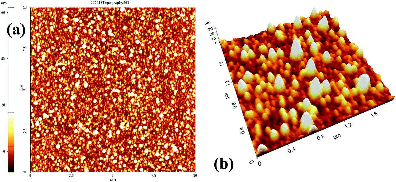 | ||
| Fig. 2 Topography of the silicon nitride thin film deposited on P–Si waver covered with tunnel silicon oxide by the PECVD process. (a) Morphology of the surface shows grain-like structures with RMS surface roughness Ra = 2.486 nm (Scanned area 10 × 10 μm2). (b) High resolution 3D-image scanned for an area of 2 × 2 μm2. | ||
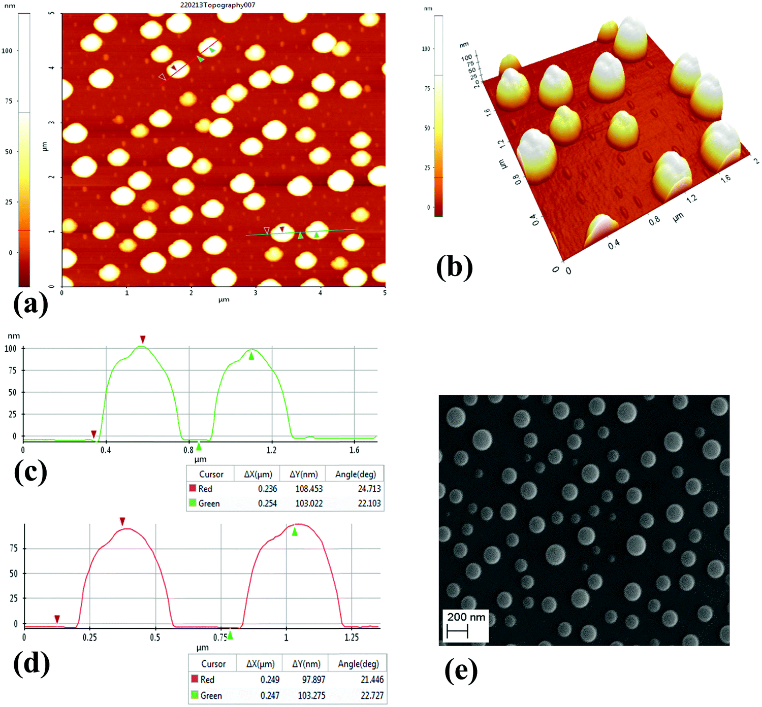 | ||
| Fig. 3 (a) Topography of selenium (Se) nanoparticles deposited on p-Si waver covered with tunnel silicon oxide scanned over for an area of 5 × 5 μm2. (b) High resolution 3D-image showing the morphology of selenium nanoparticles scanned for an area of 2 × 2 μm2. (c and d) Line profile measurements depicting the radius of nanoparticles at two different regions annotated in (a). (e) Morphology of selenium nanoparticles deposited over the tunnelling layer, revealing uniformly distributed nanoparticles. | ||
Current–voltage measurements
The current–voltage (I–V) measurements were conducted on two different devices; the reference device without selenium nanoparticles and the device with SeNPs particles were embedded between the dielectric layers. The I–V behavior of either of these devices was compared in Fig. 4. It was observed that the presence of nanoparticles leads to an enhancement of the hysteresis. This may be caused by two possible reasons. The trap charges in the nanoparticles begin to result in a building up of an internal field. Also, the rougher blocking layer plays an important role. The change in the conduction that is observed in the form of a hysteresis in Fig. 4 is due to the resultant current output either competing against or adding up with the internal field. In this case, the arrow shows the sequence of the measurement; the reverse sweep is therefore found to be more negative than the first voltage sweep. This can be attributed to the electron traps that generate an internal electric field. This internal electric field's direction is in the same direction as that of the externally applied electric field. Thus, the enhancement of the electrical field increases the current.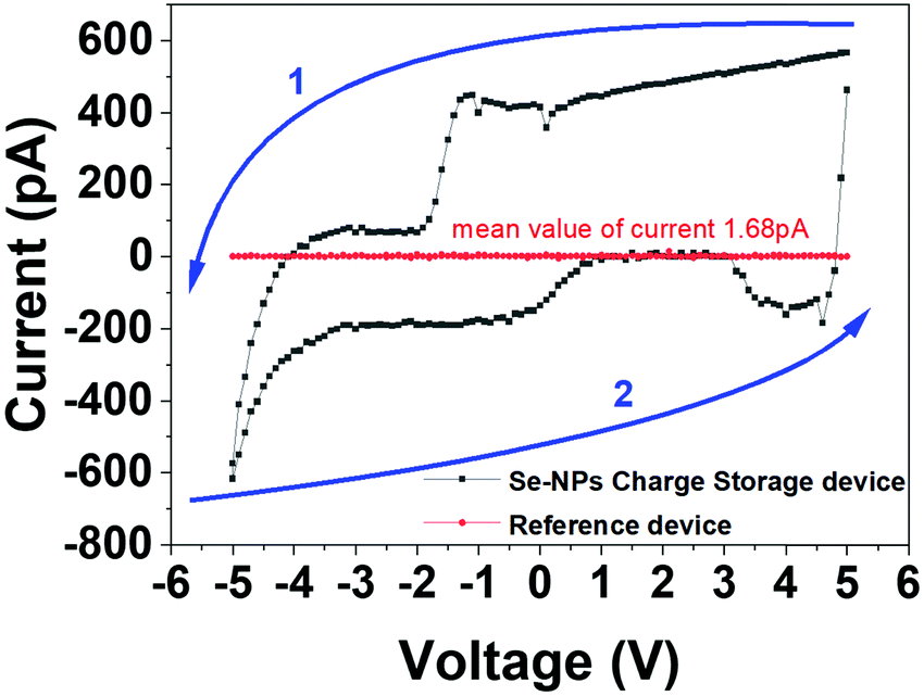 | ||
| Fig. 4 Current–voltage (I–V) characteristics of MIS devices; reference device without Se-NPs (red curve) and with Se-NPs devices (grey curve). For reference, the device mean value of the measured current is 1.68 pA. This assures the quality of the MIS structure for capacitance–voltage (C–V) measurements. | ||
The asymmetrical device structure is a deliberate attempt to enhance the tunnelling of charges mostly from one side and discourage conduction from the other side. The nanoparticles are embedded with a thicker insulator layer on one side (called the blocking layer) and a thinner insulator layer on the other side (known as the tunnelling layer) (Fig. 1).
The structure used in this study is very delicate and it is imperative to consider the maximum current that can flow through it. If the current through such structures is below few nanoamperes, the trapping and de-trapping can function well. The further increase in the current by one or two orders (to boost the ON/OFF ratio) can introduce localized heating and result in device structure modification. It can even lead to the coagulation of nanoparticles and soft dielectric breakdown.84 As the magnitude of current through the device further increases, the electronic conduction can be effected by thermal effect and the associated switching behaviors.85 The balance between lower values of ON/OFF ratio is therefore considered very carefully to ensure reliability and repeatability in CV measurements, which are divided into two distinct sections that focus on different parameters. First, the effect of the applied DC bias was analyzed (Section 4.3.1), and the effect of the variable frequency of applied AC bias is the second focus (Section 4.3.2).
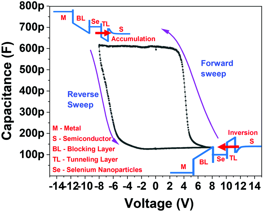 | ||
| Fig. 5 Capacitance–voltage behavior of selenium nanoparticle-based charge storage memory device. Arrows show the sequence of the measurement. Trapping and de-trapping of charges in the accumulation and inversion region, respectively, have been detailed in the illustration. | ||
This process, as can be expected, is sensitive to the magnitude of the applied bias and the width of the sweep window. This dependence was tested by progressively increasing the sweep window from ±1 V to ±10 V. The resultant CV curve have been plotted in Fig. 6a. The device achieves accumulation at about −2 V and then the accumulation capacitance extends until −10 V. The magnitude of accumulation capacitance was separately analyzed and plotted (refer Fig. 6b). A variation of 20 pF was observed in the accumulation capacitance through a range of incremental biases. This variation is acceptable; however, a greater degree of variation would point toward an onset of dielectric breakdown or trap states within the insulating layer. These measurements therefore affirm the dielectric stability under the range of applied DC-bias.
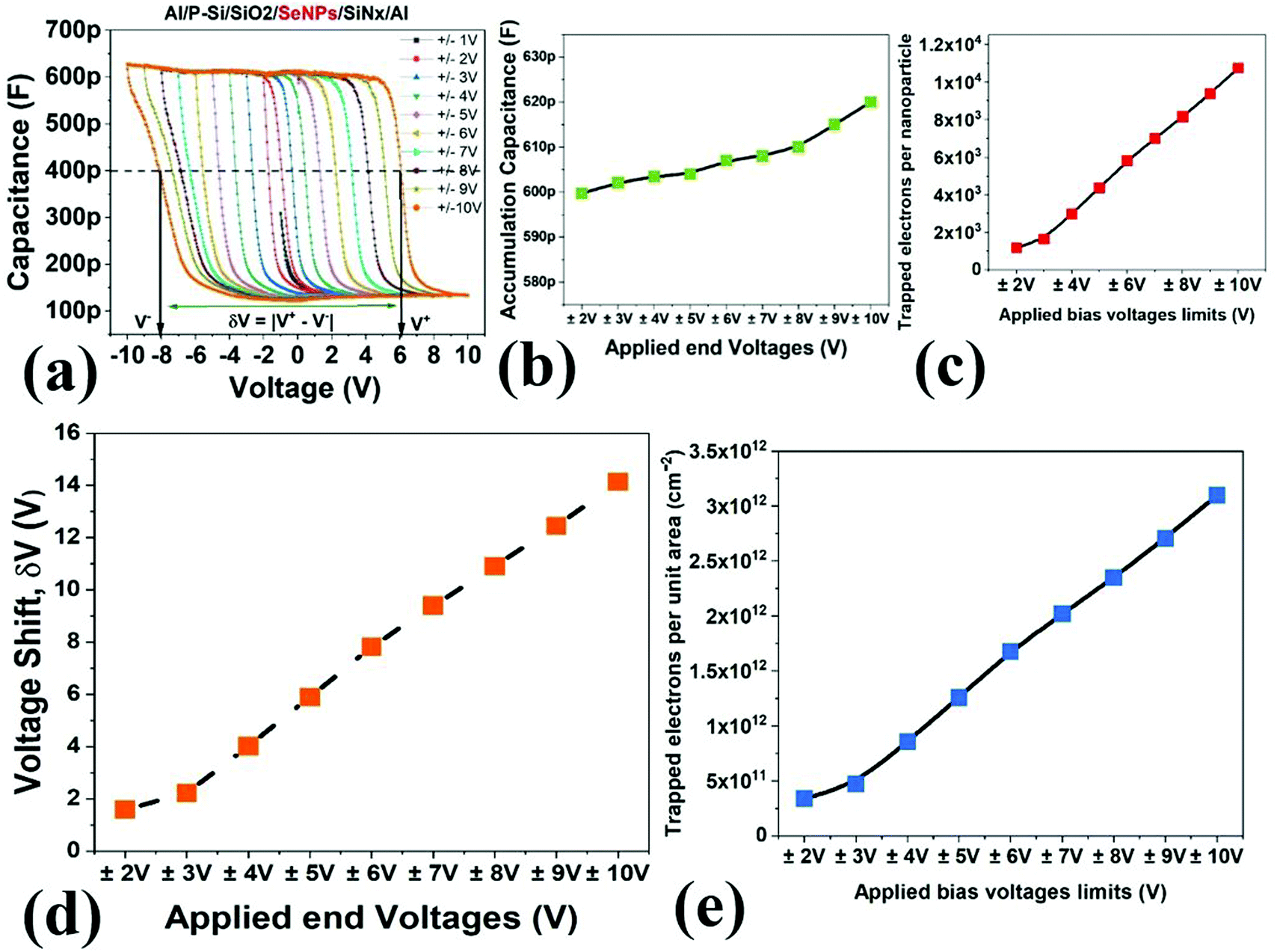 | ||
| Fig. 6 (a) Capacitance–voltage (CV) characteristics as a function of the DC bias sweep window (from ±1 V to ±10 V) for the SeNPs charge storage device. During these measurements, the AC voltage was fixed at 100 mV rms at 500 kHz. (b) Accumulation capacitance plot against the sweep window, (c) number of trapped electrons per nanoparticle plotted against applied bias. (d) Flatband voltage shift plotted as a function of sweep window, and (e) electron density/area against the sweep window. | ||
The hysteresis in the CV curve with varying bias was calculated using the flatband shift (δV); this was estimated by evaluating the difference between the forward sweep voltage (V+) and the reverse sweep voltage (V−), as can be seen in Fig. 6a.86 As expected, the flatband shift is a function of the trapped charge (refer Fig. 6c).87
Furthermore, the number of trapped charges were calculated per unit area (n) per unit area using the following relation
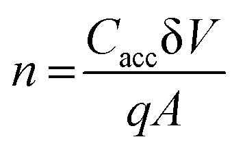 | (1) |
| δV = |Vr − Vf| | (2) |
The trap charges per unit area was obtained and is plotted in Fig. 6d, which shows a direct proportionality relationship with the magnitude of the applied bias. As the bias voltage is increased, the magnitude of the tunnelled charges increases and, consequently, the trap charges density increases. By estimating the number of electrons trapped per unit area and the number of nanoparticles per unit area, we calculated the total number of electrons trapped in a single nanoparticle. As the number of trapped electrons is a function of applied voltage, it was calculated and plotted for different bias voltages, as shown in Fig. 6c. However, it must be noted that the accuracy of the trapped electrons per nanoparticle may be affected by additional factors such as trapping of electrons in the insulator, or varying nanoparticle distribution density and spread of Gaussian distribution of the nanoparticle diameter. In our calculations, we have assumed that all the electrons, which tunnel through the oxide layer, are stored on the nanoparticles.
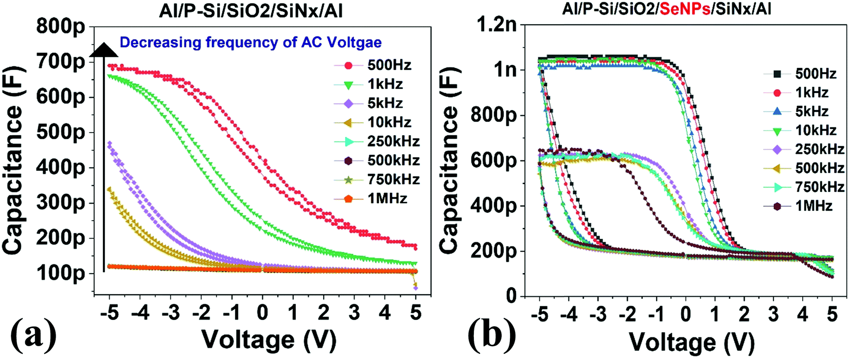 | ||
| Fig. 7 Capacitance–voltage characteristics of the (a) reference device and (b) charge storage device containing Se-NPs. The measurements were conducted at 100 mV rms. | ||
The flatband shift was calculated for the CV measurements, wherein the shift magnitude was calculated for varying frequencies (refer to Fig. 8c). The flatband shift was found to be affected by the frequency; the shift window was observed to decrease as the frequency of the applied AC signal increased. The reduction of the flatband voltage can point toward a reduction in the number of tunnelling charges. The accumulation capacitance value drops in the same manner as the reduction in the flatband voltage. However, the dip in the accumulation capacitance begins to occur much earlier. Fig. 8b shows a reduction of about 50% as the frequency is reduced from 10 kHz to 100 kHz. This could be due to the response by the dielectric layer at the frequency, which leads to an overall reduction in the capacitance of the system88 and inherent deep-energy states within the dielectric energy gap. These deep-energy states can be a function of the frequency and they may not respond to a higher frequency.
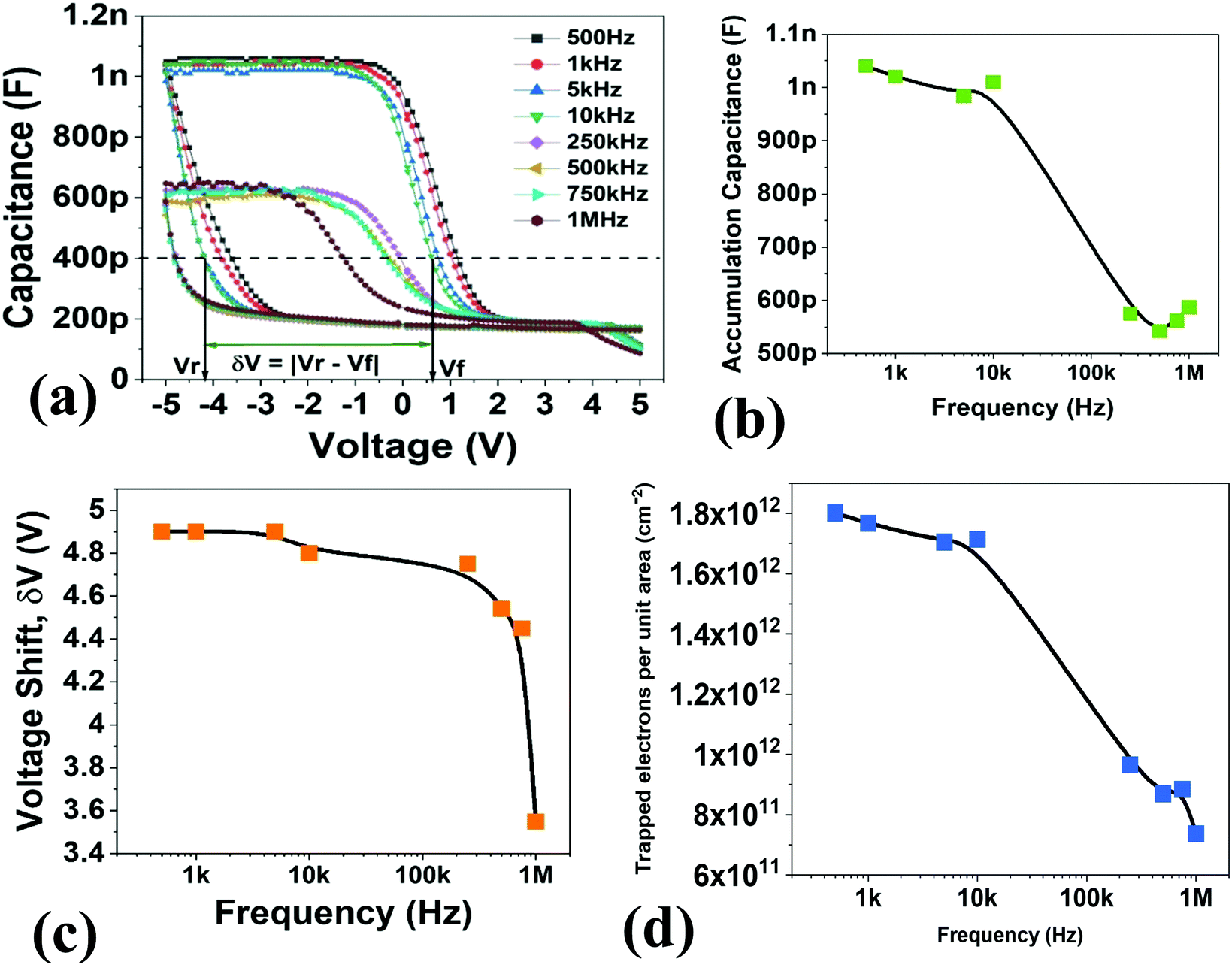 | ||
| Fig. 8 (a) Capacitance–voltage characteristics as a function of applied AC voltage frequency for the charge storage device measured at 100 mV rms. (b) Deduced accumulation capacitance, (c) voltage shift, and (d) electron density/area at different frequencies. | ||
Apart from the accumulation capacitance and the flatband voltage shift, it was observed that the trap density also reduced as the frequency increased (refer to Fig. 8d). Contributing factors from the slower charge impurities and the dielectric response of the device might lead to a reduction in the trap charge density per unit area. The frequency of the applied bias is therefore a parameter that must be considered carefully for optimum performance.
Retention (C–t) measurement
The retention measurements were also conducted, as shown in Fig. 9a. The measurements were conducted at a read voltage of 0.1 Vdc, while writing at −5 Vdc and erasing at +5 Vdc were carried out. The effective trapping of electrons results in the build-up of an internal field within the device. It is this internal field that the ‘read’ operation relies on to distinguish one state from the other. The ‘read’ operation is performed by applying the same bias that is optimized to be small enough to not influence the state of the system but still large enough to obtain a distinguishable difference between the two states. Finding an optimum value for the read bias is crucial; if it is too large, the reading of the states (“0” or “1”) will influence the escape of the trapped electrons, thereby affecting the state of the system. If it is too small, distinguishing one state from the other becomes difficult. The read bias serves primarily to be employed as a test charge to detect the presence or absence of charges in the nanoparticles. In case of presence of trapped electrons, the application of the read bias results in a small yet considerable difference in the device conduction. In this case, distinct states were observed even up to 10![[thin space (1/6-em)]](https://www.rsc.org/images/entities/char_2009.gif) 000 seconds. The loss of the charges could be due to the denser distribution of the nanoparticles, wherein a few nanoparticles are in contact with each other, which leads to charge coupling and accelerates the leaking of the charges.89 The appropriate thickness of the tunnel layer must also be further optimized. Fig. 9b shows the scatter interval plot of state “1” and state “0”. It is just to show that the two states distinguish themselves over 10000 seconds. The Euclidean distance between the state means and the Bhattacharyya ((DB(p,q)) distance is nonzero; therefore, the states are distinguishable.
000 seconds. The loss of the charges could be due to the denser distribution of the nanoparticles, wherein a few nanoparticles are in contact with each other, which leads to charge coupling and accelerates the leaking of the charges.89 The appropriate thickness of the tunnel layer must also be further optimized. Fig. 9b shows the scatter interval plot of state “1” and state “0”. It is just to show that the two states distinguish themselves over 10000 seconds. The Euclidean distance between the state means and the Bhattacharyya ((DB(p,q)) distance is nonzero; therefore, the states are distinguishable.
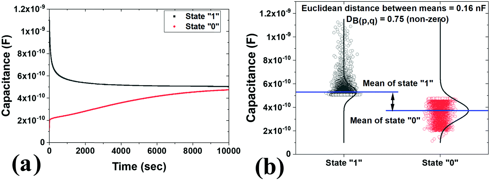 | ||
| Fig. 9 Charge retention data of charge storage undertaken over a period of time. Charge was stored (data write) by applying +5 Vdc and removed (data-erase) by applying 5 Vdc, stored charge was measured (data-read) at 0.1 Vdc and 100 mV rms set at 500 kHz. (b) An interval plot showing state “1” and state “0”; the plot provides information whether the two states have similar mean values and also provides a comparison of the amount of variation present in each state. We assumed normal distribution, for simplicity, in each state for determining the Euclidean and Bhattacharyya distance. | ||
Conclusion
In this study, selenium nanoparticles embedded in insulating matrix devices were tested and studied to identify the evidence of charge storage. The presence of nanoparticles was found to be essential for electrical switching between two conductive states. The I–V and C–V curve also evidenced an enhanced hysteresis in the SeNP devices; a minimum hysteresis was observed in the reference device. The flatband voltage shift was found to have a proportional relationship with the bias voltage. The accumulation capacitance maintained a fairly steady value through the range of bias sweep window, indicating no dielectric breakdown. The trap charge density and the flatband voltage, however, reduced as the frequency of the applied AC signal increased. This is attributed to the presence of deep energy states within the insulating nanoparticles, being unable to follow a higher applied frequency. Retention measurement was conducted for the MIS device, demonstrating distinct capacitance states. Both the Euclidean and Bhattacharyya distance are nonzero; thus, the states (“0” and “1”) are distinguishable.Conflicts of interest
There are no conflicts to declare.References
- M. Di Ventra and Y. V. Pershin, “Memory materials: a unifying description”, Mater. Today, 2011, 14(12), 584–591 CrossRef.
- M. Di Ventra and Y. V. Pershin, “Memory materials: A unifying description”, Mater. Today, 2011, 14(12), 584–591, DOI:10.1016/S1369-7021(11)70299-1.
- B. Hwang and J. S. Lee, “Recent Advances in Memory Devices with Hybrid Materials”, Adv. Electron. Mater., 2019, 5(1), 1–22, DOI:10.1002/aelm.201800519.
- J. S. Meena, S. M. Sze, U. Chand and T. Y. Tseng, “Overview of emerging nonvolatile memory technologies”, Nanoscale Res. Lett., 2014, 9(1), 1–33, DOI:10.1186/1556-276X-9-526.
- D. Prime and S. Paul, “Overview of organic memory devices”, Philos. Trans. R. Soc., A, 2009, 367(1905), 4141–4157, DOI:10.1098/rsta.2009.0165.
- D. Prime and S. Paul, “Gold nanoparticle based electrically rewritable polymer memory devices” CIMTEC 2008 - Proc. 3rd Int. Conf. Smart Mater. Struct. Syst. - Smart Mater. Micro/Nanosystems, 54, 480–485, 2008 DOI:10.4028/www.scientific.net/AST.54.480.
- Q. D. Ling, D. J. Liaw, C. Zhu, D. S.-H. Chan, E. T. Kang and K. G. Neoh, “Polymer electronic memories: Materials, devices and mechanisms”, Prog. Polym. Sci., 2008, 33(10), 917–978, DOI:10.1016/j.progpolymsci.2008.08.001.
- V. Suresh, D. Y. Kusuma, P. S. Lee, F. L. Yap, M. P. Srinivasan and S. Krishnamoorthy, “Hierarchically built gold nanoparticle supercluster arrays as charge storage centers for enhancing the performance of flash memory devices”, ACS Appl. Mater. Interfaces, 2015, 7(1), 279–286, DOI:10.1021/am506174s.
- N. Derhacobian, S. C. Hollmer, N. Gilbert and M. N. Kozicki, “Power and Energy Perspectives of Nonvolatile Memory Technologies Memory cells that store information by modulating the resistance of a dielectric may provide nonvolatile memory for next-generation ultralow-energy applications” 2010.
- A. Chen, “A review of emerging non-volatile memory (NVM) technologies and applications”, Solid. State. Electron., 2016, 125, 25–38, DOI:10.1016/j.sse.2016.07.006.
- Y. Yang, J. Ouyang, L. Ma, R. Tseng and C. Chu, “Electrical switching and bistability in organic/polymeric thin films and memory devices”, Adv. Funct. Mater., 2006, 16(8), 1001–1014 CrossRef CAS.
- T. C. Chang, K. C. Chang, T. M. Tsai, T. J. Chu and S. M. Sze, “Resistance random access memory”, Mater. Today, 2016, 19(5), 254–264, DOI:10.1016/j.mattod.2015.11.009.
- S. Lombardo, B. De Salvo, C. Gerardi and T. Baron, “Silicon nanocrystal memories”, Microelectron. Eng., 2004, 72(1–4), 388–394, DOI:10.1016/j.mee.2004.01.020.
- Z. Liu, C. Lee, V. Narayanan, G. Pei and E. C. Kan, “Metal nanocrystal memories - Part II: Electrical characteristics”, IEEE Trans. Electron Devices, 2002, 49(9), 1614–1622, DOI:10.1109/TED.2002.802618.
- Z. Liu, C. Lee, V. Narayanan, G. Pei and E. C. Kan, “Metal nanocrystal memories - Part I: Device design and fabrication”, IEEE Trans. Electron Devices, 2002, 49(9), 1606–1613, DOI:10.1109/TED.2002.802617.
- K. Qian, V. C. Nguyen, T. Chen and P. S. Lee, “Novel concepts in functional resistive switching memories”, J. Mater. Chem. C, 2016, 4(41), 9637–9645, 10.1039/c6tc03447k.
- Y. Li, et al., “Recent advances in organic-based materials for resistive memory applications”, InfoMat, 2020, 2(6), 995–1033, DOI:10.1002/inf2.12120.
- L. D. Bozano, B. W. Kean, M. Beinhoff, K. R. Carter, P. M. Rice and J. C. Scott, “Organic materials and thin-film structures for cross-point memory cells based on trapping in metallic nanoparticles”, Adv. Funct. Mater., 2005, 15(12), 1933–1939, DOI:10.1002/adfm.200500130.
- L. Ma, J. Liu, S. Pyo, Q. Xu and Y. Yang, “Organic bistable devices”, Mol. Cryst. Liq. Cryst. Sci. Technol., Sect. A, 2002, 378, 185–192, DOI:10.1080/713738589.
- S. Nau, S. Sax and E. J.-W. List-Kratochvil, “Unravelling the nature of unipolar resistance switching in organic devices by utilizing the photovoltaic effect”, Adv. Mater., 2014, 26(16), 2508–2513 CrossRef CAS PubMed.
- J. C. Scott and L. D. Bozano, “Nonvolatile memory elements based on organic materials”, Adv. Mater., 2007, 19(11), 1452–1463, DOI:10.1002/adma.200602564.
- J. Ouyang, Emerging Resistive Switching Memories. Springer, 2016.
- D. Tondelier, K. Lmimouni, D. Vuillaume, C. Fery and G. Haas, “Metal/organic/metal bistable memory devices”, Appl. Phys. Lett., 2004, 85(23), 5763–5765, DOI:10.1063/1.1829166.
- S. Chaudhary and S. K. Mehta, “Selenium nanomaterials: Applications in electronics, catalysis and sensors”, J. Nanosci. Nanotechnol., 2014, 14(2), 1658–1674, DOI:10.1166/jnn.2014.9128.
- T. Fan, Z. Xie, W. Huang, Z. Li and H. Zhang, “Two-dimensional non-layered selenium nanoflakes: facile fabrications and applications for self-powered photo-detector”, Nanotechnology, 2019, 30(11), 114002, DOI:10.1088/1361-6528/aafc0f.
- C. Xing, et al., 2D Nonlayered Selenium Nanosheets: Facile Synthesis, Photoluminescence, and Ultrafast Photonics”, Adv. Opt. Mater., 2017, 5(24), 1700884, DOI:10.1002/adom.201700884.
- W. Huang, et al., “Enhanced Photodetection Properties of Tellurium@Selenium Roll-to-Roll Nanotube Heterojunctions”, Small, 2019, 15(23), 1900902, DOI:10.1002/smll.201900902.
- J. L. Hartke and P. J. Regensburger, “Electronic States in Vitreous Selenium”, Phys. Rev., 1965, 139(3A), A970–A980, DOI:10.1103/PhysRev.139.A970.
- J. L. Hartke, “Drift Mobilities of Electrons and Holes and Space-Charge-Limited Currents in Amorphous Selenium Films”, Phys. Rev., 1962, 125(4), 1177–1192, DOI:10.1103/PhysRev.125.1177.
- P. H. Yeh, L. J. Chen, P. T. Liu, D. Y. Wang and T. C. Chang, “Metal nanocrystals as charge storage nodes for nonvolatile memory devices”, Electrochim. Acta, 2007, 52(8), 2920–2926, DOI:10.1016/j.electacta.2006.09.006.
- D. Qin, H. Tao, Y. Zhao, L. Lan, K. Chan and Y. Cao, “Field effect transistor from individual trigonal Se nanowire”, Nanotechnology, 2008, 19(35), 355201, DOI:10.1088/0957-4484/19/35/355201.
- S. Alotaibi, K. Nama Manjunatha and S. Paul, “A study of selenium nanoparticles as charge storage element for flexible semi-transparent memory devices”, Appl. Surf. Sci., 2017, 424, 330–336, DOI:10.1016/j.apsusc.2017.03.091.
- F. Paul and S. Paul, “To Be or Not to Be – Review of Electrical Bistability Mechanisms in Polymer Memory Devices”, Small, 2022, 2106442, DOI:10.1002/smll.202106442.
- S. Pyo, L. Ma, J. He, Q. Xu, Y. Yang and Y. Gao, “Experimental study on thickness-related electrical characteristics in organic/metal-nanocluster/organic systems”, J. Appl. Phys., 2005, 98, 5, DOI:10.1063/1.2033142.
- J. He, L. Ma, J. Wu and Y. Yang, “Three-terminal organic memory devices”, J. Appl. Phys., 2005, 97, 6, DOI:10.1063/1.1866496.
- Y. Yang, L. Ma and J. Wu, “Organic thin-film memory”, MRS Bull., 2004, 29(11), 833–837 CrossRef CAS.
- L. Ma, J. Liu, S. Pyo and Y. Yang, “Organic bistable light-emitting devices”, Appl. Phys. Lett., 2002, 80(3), 362–364, DOI:10.1063/1.1436274.
- L. Ma, S. Pyo, J. Ouyang, Q. Xu and Y. Yang, “Nonvolatile electrical bistability of organic/metal-nanocluster/organic system”, Appl. Phys. Lett., 2003, 82(9), 1419–1421, DOI:10.1063/1.1556555.
- L. P. Ma, J. Liu and Y. Yang, “Organic electrical bistable devices and rewritable memory cells”, Appl. Phys. Lett., 2002, 80(16), 2997–2999, DOI:10.1063/1.1473234.
- J. Wu, L. Ma and Y. Yang, “Single-band Hubbard model for the transport properties in bistable organic/metal nanoparticle/organic devices”, Phys. Rev. B: Condens. Matter Mater. Phys., 2004, 69(11), 115321 CrossRef.
- C. Barriac, P. Pinard and F. Davoine, “Electrical Properties OF Al-Al203-Metal Structures”, Phys. Status Solidi, 1969, 34(2), 621 CrossRef.
- T. W. Hickmott, “Low-frequency negative resistance in thin anodic oxide films”, J. Appl. Phys., 1962, 33(9), 2669–2682 CrossRef CAS.
- D. S. Jeong, et al., “Emerging memories: Resistive switching mechanisms and current status”, Rep. Prog. Phys., 2012, 75(7), 076502, DOI:10.1088/0034-4885/75/7/076502.
- J. G. Simmons and R. R. Verderber, “New Thin-film Resistive Memory”, Radio Electron. Eng., 1967, 34(2), 81–89, DOI:10.1049/ree.1967.0069.
- J. G. Simmons and R. R. Verderber, “New conduction and reversible memory phenomena in thin insulating films”, Proc. R. Soc. London, Ser. A, 1967, 301(1464), 77–102 CAS.
- Y. T. You, M. L. Wang, H. N. Xuxie, B. Wu, Z. Y. Sun and X. Y. Hou, “Conductance-dependent negative differential resistance in organic memory devices”, Appl. Phys. Lett., 2010, 97(23), 261 CrossRef.
- M. Lauters, B. McCarthy, D. Sarid and G. E. Jabbour, “Multilevel conductance switching in polymer films”, Appl. Phys. Lett., 2006, 89(1), 10–13, DOI:10.1063/1.2219338.
- H. Houili, E. Tutiš and R. Izquierdo, “Modeling nanoparticle embedded organic memory devices”, Org. Electron., 2010, 11(4), 514–520, DOI:10.1016/j.orgel.2009.12.006.
- S. Song, et al., “Twistable nonvolatile organic resistive memory devices”, Org. Electron., 2013, 14(8), 2087–2092, DOI:10.1016/j.orgel.2013.05.003.
- D. Lee, et al., “Resistance switching of the nonstoichiometric zirconium oxide for nonvolatile memory applications”, IEEE Electron Device Lett., 2005, 26(10), 719–721 CAS.
- J. D. Lee, H. M. Seung, K. C. Kwon and J. G. Park, “Dependence of nonvolatile memory characteristics on curing temperature for polymer memory-cell embedded with Au nanocrystals in poly(N-vinylcarbazole)”, Curr. Appl. Phys., 2011, 11(2 SUPPL.), e25–e29, DOI:10.1016/j.cap.2010.12.037.
- J. Chen, L. Xu, J. Lin, Y. Geng, L. Wang and D. Ma, “Negative differential resistance effect in organic devices based on an anthracene derivative”, Appl. Phys. Lett., 2006, 89(8), 83514 CrossRef.
- R. J. Tseng, J. Ouyang, C.-W. Chu, J. Huang and Y. Yang, “Nanoparticle-induced negative differential resistance and memory effect in polymer bistable light-emitting device”, Appl. Phys. Lett., 2006, 88(12), 123506 CrossRef.
- W. Tang, et al., “Memory Effect and Negative Differential Resistance by Electrode-Induced Two-Dimensional Single-Electron Tunneling in Molecular and Organic Electronic Devices”, Adv. Mater., 2005, 17(19), 2307–2311 CrossRef CAS.
- J. Lin and D. Ma, “Origin of negative differential resistance and memory characteristics in organic devices based on tris (8-hydroxyquinoline) aluminum”, J. Appl. Phys., 2008, 103(12), 124505 CrossRef.
- S. M. Islam, P. Banerji and S. Banerjee, “Electrical bistability, negative differential resistance and carrier transport in flexible organic memory device based on polymer bilayer structure”, Org. Electron., 2014, 15(1), 144–149 CrossRef CAS.
- C.-H. Tu, D.-L. Kwong and Y.-S. Lai, “Negative differential resistance and electrical bistability in nanocrystal organic memory devices”, Appl. Phys. Lett., 2006, 89(25), 252107 CrossRef.
- M. Xie, K. C. Aw, M. Langlois and W. Gao, “Negative differential resistance of a metal-insulator-metal device with gold nanoparticles embedded in polydimethylsiloxane”, Solid State Commun., 2012, 152(10), 835–838, DOI:10.1016/j.ssc.2012.02.023.
- L. D. Bozano, B. W. Kean, V. R. Deline, J. R. Salem and J. C. Scott, “Mechanism for bistability in organic memory elements”, Appl. Phys. Lett., 2004, 84(4), 607–609, DOI:10.1063/1.1643547.
- R. R. Vekderber, B. Eales and J. G. Simmons, “Forming process in evaporated SiO thin films”, Philos. Mag., 1967, 16(143), 1049–1061, DOI:10.1080/14786436708229693.
- D. P. Oxley, “Electroforming, Switching and Memory Effects in Oxide Thin Films” Electrocompon, Sci. Technol., 1977, 3(4), 217–224, DOI:10.1155/APEC.3.217.
- R. R. Sutherland, “A theory for negative resistance and memory effects in thin insulating films and its application to Au-ZnS-Au devices”, J. Phys. D. Appl. Phys., 1971, 4(3), 468–479, DOI:10.1088/0022-3727/4/3/318.
- T. W. Kim, Y. Yang, F. Li and W. L. Kwan, “Electrical memory devices based on inorganic/organic nanocomposites”, NPG Asia Mater., 2012, 4(6), e18–e18 CrossRef.
- J. Ouyang, C. W. Chu, C. R. Szmanda, L. Ma and Y. Yang, “Programmable polymer thin film and non-volatile memory device”, Nat. Mater., 2004, 3(12), 918–922, DOI:10.1038/nmat1269.
- J. Ouyang, C. W. Chu, D. Sieves and Y. Yang, “Electric-field-induced charge transfer between gold nanoparticle and capping 2-naphthalenethiol and organic memory cells”, Appl. Phys. Lett., 2005, 86(12), 1–3, DOI:10.1063/1.1887819.
- C. W. Chu, J. Ouyang, J. Tseng and Y. Yang, “Organic donor–acceptor system exhibiting electrical bistability for use in memory devices”, Adv. Mater., 2005, 17(11), 1440–1443 CrossRef CAS PubMed.
- R. Tseng, J. Huang, J. Ouyang, R. B. Kaner and Y. Yang, “Gold nanoparticle/polyaniline nanofiber memory”, Nano Lett., 2005, 5, 1077–1080 CrossRef CAS PubMed.
- S. Tiwari, F. Rana, H. Hanafi, A. Hartstein, E. F. Crabbé and K. Chan, “A silicon nanocrystals based memory”, Appl. Phys. Lett., 1995, 1377, 1377, DOI:10.1063/1.116085.
- S. Paul, “Realization of nonvolatile memory devices using small organic molecules and polymer”, IEEE Trans. Nanotechnol., 2007, 6(2), 191–195, DOI:10.1109/TNANO.2007.891824.
- D. Prime and S. Paul, “Making plastic remember: Electrically rewritable polymer memory devices”, Mater. Res. Soc. Symp. Proc., 2007, 997, 21–25, DOI:10.1557/proc-0997-i03-01.
- K. Saranti and S. Paul, “e-Information on Wires: A First Step toward Two-Terminal Silicon Nanowires for Electronic Memory Devices”, ACS Appl. Electron. Mater., 2019, 1(10), 2018–2024, DOI:10.1021/acsaelm.9b00331.
- K. Saranti, S. Alotaibi and S. Paul, “A new approach for two-terminal electronic memory devices - Storing information on silicon nanowires”, Sci. Rep., 2016, 6, 1–8, DOI:10.1038/srep27506.
- K. Saranti and S. Paul, “Charge-Trap-Non-volatile Memory and Focus on Flexible Flash Memory Devices” in Charge-Trapping Non-Volatile Memories, Springer, 2017, pp. 55–89 Search PubMed.
- I. Salaoru and S. Paul, “Electrically re-writable non-volatile memory device - Using a blend of sea salt and polymer” CIMTEC 2008 - Proc. 3rd Int. Conf. Smart Mater. Struct. Syst. - Smart Mater. Micro/Nanosystems, 54, 486–490, 2008 DOI:10.4028/www.scientific.net/AST.54.486.
- I. Salaoru, S. P. Iulia Salaoru, Z. Al Halafi and S. Paul, “Creating Electrical Bistability Using Nano-bits – Application in 2-Terminal Memory Devices”, MRS Adv., 2017, 357, 195–208, DOI:10.1557/adv.2016.677.
- I. Salaoru and S. Paul, “Small Organic Molecules for Electrically Re-writable Non-volatile Polymer Memory Devices”, Mater. Res. Soc. Symp. Proc., 2010, 1250, 159–164, DOI:10.1557/PROC-1250-G04-11.
- A. Kanwal, S. Paul and M. Chhowalla, “Organic memory devices using C 60 and insulating polymer”, Mater. Res. Soc. Symp. Proc., 2005, 830, 349–353 CAS.
- S. Paul and I. Salaoru, “Electronic polymer memory devices-Easy to fabricate, difficult to understand”, Thin Solid Films, 2010, 519(2), 587–590, DOI:10.1016/j.tsf.2010.07.004.
- D. Prime and S. Paul, “First contact-charging of gold nanoparticles by electrostatic force microscopy”, Appl. Phys. Lett., 2010, 96, 4, DOI:10.1063/1.3300731.
- D. Prime, S. Paul and P. W. Josephs-Franks, “Electrical properties of nanometre thin film polystyrene for organic electronic applications”, IEEE Trans. Dielectr. Electr. Insul., 2008, 15(4), 905–909, DOI:10.1109/TDEI.2008.4591208.
- D. C. Prime, Z. Al Halafi, M. A. Green, I. Salaoru and S. Paul, “Electrical Conductivity Bistability in Nano-Composite”, ECS Trans., 2013, 53(4), 141–148, DOI:10.1149/05304.0141ecst.
- I. Salaoru and S. Paul, “Bistability in electrically writable non-volatile polymer memory devices”, Mater. Res. Soc. Symp. Proc., 2008, 1114, 100–105, DOI:10.1557/proc-1114-g12-09.
- D. Black, S. Paul and I. Salaoru, “Ferroelectric nanoparticles in polyvinyl acetate (PVAc) matrix-A method to enhance the dielectric constant of polymers”, Nanosci. Nanotechnol. Lett., 2010, 2(1), 41–45, DOI:10.1166/nnl.2010.1045.
- T. Zhang, et al., “Physical mechanisms involved in the formation and operation of memory devices based on a monolayer of gold nanoparticle-polythiophene hybrid materials”, Nanoscale Adv., 2019, 1(7), 2718–2726, 10.1039/c9na00285e.
- D. S. Jeong, et al., “Emerging memories: Resistive switching mechanisms and current status”, Rep. Prog. Phys., 2012, 75, 7, DOI:10.1088/0034-4885/75/7/076502.
- S. Paul, et al., “Langmuir-Blodgett film deposition of metallic nanoparticles and their application to electronic memory structures”, Nano Lett., 2003, 3(4), 533–536, DOI:10.1021/nl034008t.
- D. Prime and S. Paul, “Electrical and morphological properties of polystyrene thin films for organic electronic applications”, Vacuum, 2010, 84(10), 1240–1243, DOI:10.1016/j.vacuum.2009.10.033.
- S. M. Sze, Y. Li and K. K. Ng, Physics of semiconductor devices. John wiley & sons, 2021 Search PubMed.
- G. Schön and U. Simon, “A fascinating new field in colloid science: small ligand-stabilized metal clusters and possible application in microelectronics - Part I: State of the art”, Colloid Polym. Sci., 1995, 273(2), 101–117, DOI:10.1007/BF00654007.
| This journal is © The Royal Society of Chemistry 2022 |