
 Open Access Article
 This Open Access Article is licensed under a
 Creative Commons Attribution 3.0 Unported Licence
Enabling fine-grain free 2-micron thick CISe/CIGSe film fabrication via a non-hydrazine based solution processing route†
Swapnil D.
Deshmukh
 a,
Kyle G.
Weideman
a,
Ryan G.
Ellis
a,
Kim
Kisslinger
b and
Rakesh
Agrawal
*a
a,
Kyle G.
Weideman
a,
Ryan G.
Ellis
a,
Kim
Kisslinger
b and
Rakesh
Agrawal
*a
aDavidson School of Chemical Engineering, Purdue University, West Lafayette, IN 47907, USA
bCenter for Functional Nanomaterials, Brookhaven National Laboratory, Upton, NY 11973, USA
First published on 24th February 2022
Abstract
Solution processing of CuInSe2/CuInGaSe2 (CISe/CIGSe) photovoltaic devices via non-hydrazine based routes has been studied for the past few years and a significant improvement in the device performance has been achieved for multiple solvent routes. However, none of these routes have ever reported the fabrication of absorbers with a thickness of above 1.2–1.3 microns which is almost half of what has been traditionally used in vacuum based high efficiency CIGSe devices. The main reason for this limitation is associated with the formation of a fine-grain layer in solution based systems. Here we manipulate the formation of such a fine-grain layer in an amine–thiol based solution route through surface modifications at the bottom Mo interface and achieve an active area efficiency of up to 14.1% for CIGSe devices. Furthermore, with a detailed analysis of the fine-grain layer, not just in the amine–thiol based film, but also in the film fabricated via the dimethylformamide-thiourea route, we identify the reason for the formation of such a fine-grain layer as the presence of the sulfide material and carbon impurity (if any) in the precursor film. We utilize the amine–thiol solvent system's ability for selenium and metal selenide dissolution to manipulate the ink formulations and demonstrate the reduction in the formation of sulfide materials as well as the extent of trapped carbon in the precursor film. With modified precursor films, we then successfully grow CISe/CIGSe thin films of 2-micron thickness with the complete absence of a fine-grain layer through a high temperature, thickness independent bulk growth mechanism making the film morphology similar to the one fabricated using a high efficiency hydrazine based route.
Introduction
The chalcopyrite CuInGaSe2 (CIGSe) thin film photovoltaic material has reached a lab scale device efficiency of around 23.4%.1 Such high efficiency device fabrication was enabled by implementing various advances that have been studied in CIGSe systems over the past few years. Some of these advances include optimization of the absorber deposition process, developing bandgap grading in the absorber via the composition variation of gallium, changing the surface properties with surface sulfurization optimization, use of heavy alkali post-deposition treatments, optimizing the buffer layer deposition, etc.2,3 While the use of these various approaches indeed realized high performance CIGSe devices, these absorbers are typically fabricated through vacuum based deposition routes, causing potential limitations for achieving low cost, high throughput uniform module fabrication on a large scale. To overcome these challenges, researchers are working on developing a solution processing route with high device performance. Currently, the hydrazine based CIGSe thin film deposition route holds the record for the highest efficiency of a solution based CIGSe PV device with a reported value of 18.1%.4 However, due to the toxicity and explosive nature of the hydrazine solvent system, other non-hydrazine solution processing routes are being studied for the deposition of CIGSe thin films. For this, the two main methods involve the use of nanoparticles5 and molecular precursor solutions.6 Amongst the different successful molecular precursor approaches, some use protic solvents like water, alcohols, amines, thiols while others use aprotic solvents like dimethyl sulfoxide (DMSO) and dimethyl formamide (DMF).7 Recently, the amine–thiol solvent system has produced the highest efficiency non-hydrazine based solution processed device with an active area efficiency of 16.4% for CIGSe thin films.8 This solution system has also successfully demonstrated gallium grading,9 silver addition,10 and surface treatments like sulfurization11 and creating ordered vacancy compounds8 for the improvement of uniform CIGSe thin films through solution processing routes. Other than amine–thiol, routes which have produced CIGSe devices with efficiencies of around 14–15% involve the CuInGaS2 (CIGS) nanoparticles,12 alcohol based route,13 and DMF-thiourea based route.14,15While different solution processing routes are constantly improving the PV performance of CIGSe devices, one major difference in these devices compared to high efficiency vacuum based CIGSe films is the absorber thickness. All non-hydrazine solution processed films reported to date have fabricated dense absorber layers up to only 1.2–1.3 μm thickness, which is almost half of what has been used in vacuum based films. The current highest efficiency amine–thiol based device has an absorber thickness of only 900 nm with an almost 400 nm thick uncoarsened fine-grain layer sitting under the absorber grains.8 In most routes the formation of this layer is associated with the presence of impurities in the film prior to high temperature annealing which tend to get accumulated as a separate layer. The presence of such a layer and also particularly its position in the film morphology could drastically affect the film performance. As mentioned earlier, while this layer limits the thickness of the absorber material which affects both the light absorption and carrier collection, it also reduces the control over absorber composition due to non-uniform elemental distribution between these layers.
In this work, we control the morphology of CuInSe2 (CISe)/CIGSe thin films fabricated from the amine–thiol solvent system by manipulating the solution composition and substrate selection. Fabrication of the absorber material on the thin MoO3 layer instead of directly on the Mo layer leads to improvements in the device performance by altering the position of the fine-grain layer in the film architecture. This allows us to fabricate a CIGSe thin film of uniform composition with an active area efficiency of 14.1%, almost 1–2% higher than those of previously reported amine–thiol based uniform CIGSe films. Analysis of the fine-grain layer further provides insights into the traditional growth mechanism and possible cause for its formation, not just in the case of the amine–thiol based film, but for routes that rely on the selenization of sulfide precursor films. By utilizing amine–thiol solution's ability to dissolve selenium and metal selenide precursors, film compositions are altered and their effect on the contaminant concentration in the precursor film as well as the grain growth is studied. With this analysis and optimization, we demonstrate the fabrication of impurity free precursor films which are compositionally identical to hydrazine based films. This allows us to fabricate the first ever hydrazine-free 2-micron thick CISe/CIGSe absorber layer free of any fine-grain material. The modified growth mechanism leading to such morphology, however, changes the electronic properties of the film and more work is underway to understand the changes in the optoelectronic properties to utilize this solution route for high efficiency, large scale film fabrication.
Experimental section
Materials
In powder (99.999%) was purchased from STREM. Ga pellets (99.99999%) and In2Se3 (99.99%) were purchased from Alfa Aesar. Cu2S (99.99%), Se (99.99%), Cu2Se (99.95%), CuCl (99.995%), InCl3 (99.999%), thiourea (TU, >99%), butylamine (BA, 99%), 1,2-ethanedithiol (EDT, >98%), N,N-dimethylformamide (DMF, 99.8%), and acetonitrile (99.8%) were purchased from Sigma-Aldrich. All chemicals were used as received except for Ga pellets, which are scraped with a razor blade to remove a possible oxide layer on the surface prior to dissolution.Ink formulations
Amine–thiol based inks for CuInS2 (CIS) and CIGS precursor film fabrication were prepared in BA using stoichiometric additions of thiol. First In or In + Ga were dissolved in BA-EDT solution with EDT![[thin space (1/6-em)]](https://www.rsc.org/images/entities/char_2009.gif) :In or EDT:(In + Ga) ratio of 2. After complete dissolution, Cu2S powder was added to this solution along with some more EDT such as an EDT:Cu of 1. This BA based ink was used for coating films for device fabrication. For FTIR studies, some inks were prepared in acetonitrile solvent where the EDT:metal ratio was kept constant but the quantity of BA was reduced to BA:EDT of 2 instead of using BA as a bulk solvent in excess.
:In or EDT:(In + Ga) ratio of 2. After complete dissolution, Cu2S powder was added to this solution along with some more EDT such as an EDT:Cu of 1. This BA based ink was used for coating films for device fabrication. For FTIR studies, some inks were prepared in acetonitrile solvent where the EDT:metal ratio was kept constant but the quantity of BA was reduced to BA:EDT of 2 instead of using BA as a bulk solvent in excess.
Selenium containing inks were prepared by adding required quantities of elemental Se in CIS/CIGS BA-EDT ink. For metal selenide inks, Cu2Se, In2Se3, and elemental Se were added together to BA-EDT solutions to get an indium concentration of 0.2 M, Cu:In of 0.9, and EDT:(Cu + In) of 3. DMF based inks were prepared by dissolving 2.28 M thiourea in DMF solvent. After complete dissolution, InCl3 was added to this solution and stirred overnight to get a 0.4 M indium concentration. CuCl was then added to this solution to get a Cu:In ratio of 0.9. Hydrazine based ink was prepared by codissolving Cu2S, In2Se3, S and Se at room temperature with a Cu/In ratio of 0.9.
Film and device fabrication
The CIS/CIGS precursor film was fabricated by blade coating onto a 2′′ × 1′′ molybdenum coated (∼800 nm) soda lime glass (SLG) substrate using the BA-EDT ink mentioned above. Multiple layers of this ink were coated to get the desired thickness of the film. This coating was performed via a bar coating technique using an auto blade coater with a glass rod. The coating speed was around 20 mm s−1 with 2 back and forth passes per layer. After each coating, the film was immediately annealed on a pre-heated hot plate between 300 and 350 °C for 2–5 min. 10–15 nm of sodium fluoride was then deposited on top of the as-prepared precursor film by electron-beam deposition. The film was then selenized by exposing it to Se vapor in a non-pyrolytic graphite box (containing the sample and elemental Se pellets) at 500 °C for 25 min in a preheated tube furnace. Photovoltaic devices were completed by chemical bath deposition of ∼50 nm cadmium sulfide (CdS), sputtering of ∼80 nm intrinsic zinc oxide (ZnO) followed by ∼220 nm indium tin oxide (ITO), and electron-beam deposition of 100 nm Ni/1000 nm Al grids. Each device on the film was separated by mechanical scribing, defining a total area of ∼0.47 cm2. For MoO3 deposition, a thermal evaporation apparatus was used and 5–10 nm of MoO3 was deposited on a 2′′ × 1′′ molybdenum coated glass substrate.Exfoliated films were prepared by separating the films from the molybdenum substrate. This was done by gluing a sheet of 1.8 mm SLG to the CISe film surface with a quick setting two-part epoxy (Loctite, EA 9017) and mechanically separating the SLG support and the SLG/Mo substrate, exposing a clean, flat interface.
Characterization
X-Ray diffractograms (XRD) were obtained using a Rigaku Smart Lab diffractometer in Parallel-Beam mode, using a Cu Kα (λ = 1.5406 Å) source operating at 40 kV/44 mA. STEM-EDS data were collected on Talos 200X TEM containing four silicon drift detectors using a SiN grid. Raman and photoluminescence spectra were collected on a Horiba/Jobin-Yvon HR800 microscope with an excitation laser wavelength of 632.8 nm. FTIR spectra were collected on a Thermo-Nicolet Nexus 670 FTIR unit in transmission mode using NaCl crystal substrates. The bulk composition was analyzed using a Fisher XAN 250 X-ray fluorescence (XRF) instrument at 50 kV voltage with a primary Ni filter containing a silicon drift detector. A FEI Quanta 3D FEG Dual-beam SEM was used to obtain the micrographs of the films. The J–V characteristics were measured on a four-point probe station using a Keithley 2400 series source meter while the sample rested on a temperature-controlled stage at 25 °C. Illumination was provided by a Newport Oriel solar simulator with an AM1.5 filter set and calibrated to 1 sun intensity using a Si reference cell certified by NIST.Results and discussion
Location of the fine-grain layer
Stoichiometric quantities of amine and thiol were used for dissolution of metal precursors (Cu2S, In and Ga) to avoid the presence of any unreacted excess amine and thiol in the solution. Inks obtained with these dissolutions were then used to fabricate precursor thin films of a sulfide material by blade coating the solution on a glass substrate. Coated liquid films were then annealed in an inert nitrogen atmosphere at different temperatures to study the removal of organic solvents. FTIR data collected on these films showed complete removal of organic residues (i.e. C–H stretching between 2800–3000 cm−1) for a temperature of 350 °C (Fig. 1). To verify whether the solvent used for film fabrication plays any role in determining the minimum temperature for the removal of organic residues from the film, two different solvents, butylamine and acetonitrile were used for film fabrication. However, both the solvents showed identical results at different temperatures suggesting that the metal thiolates formed in the solution are the primary source of organic residues in the films annealed at lower temperatures.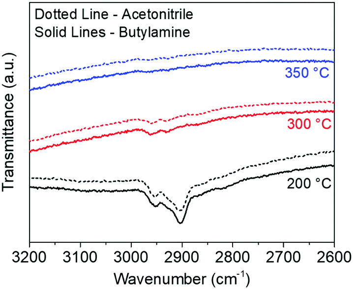 | ||
| Fig. 1 FTIR data collected on CIS films coated with two different solvents, acetonitrile and butylamine, annealed at different temperatures. | ||
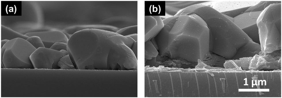
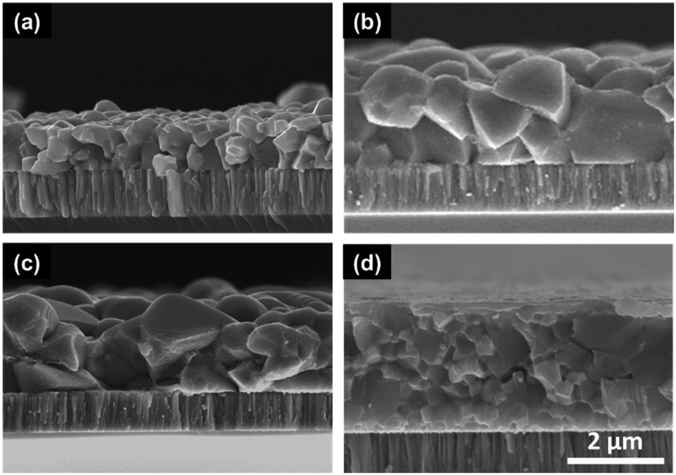
After identifying the minimum temperature required for removal of organic residues, CIS films of around 1-micron thickness were fabricated on Mo coated SLG substrate and selenized in a tube furnace at 500 °C for 25 min under selenium atmosphere. XRD and Raman spectra on this film confirm the formation of chalcopyrite CISe phase in the absence of any secondary material (Fig. S1, ESI†). However, the SEM cross-section shows the formation of a trilayer morphology with a fine-grain layer sandwiched between two CISe grain layers (Fig. 2a). This observation is consistent for gallium containing films, i.e. selenized CIGS precursor films (Fig. S2, ESI†). Traditionally, CIGS nanoparticle films have been shown to grow from the top surface giving a bilayer morphology with larger grains at the top and a fine-grain layer at the Mo interface12,16,17 while the films from DMF/DMSO–TU based routes and previous amine–thiol based routes have shown to grow from both top and bottom giving 2 grain morphology.14,18,19 The reason for the difference in grain growth between two different routes could be related to the solvents used for film fabrication or the extent of organic residue remaining in the film prior to selenization which could affect the nucleation from the Mo interface. For the case where grains are growing from the bottom, the Mo surface must be acting as a nucleation center for CISe grains. To understand the role of the substrate, a CIS film was deposited directly on glass and selenized under similar conditions. As can be seen from Fig. 2b, the selenized film shows grain formation only from the top surface with a fine-grain layer near the glass interface. This confirms that the Mo interface indeed serves as a nucleation site for CISe grains.
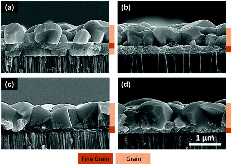 | ||
| Fig. 2 Cross-sectional SEM images of selenized CIS film coated (a) on molybdenum, (b) directly on glass, (c) on 10 nm MoO3 coated molybdenum, and (d) on 5 nm MoO3 coated molybdenum. | ||
A similar phenomenon was observed in the literature for Cu2ZnSnSe4 (CZTSe) thin films fabricated via selenization of sulfide Cu2ZnSnS4 (CZTS) films. A film deposited on the Mo substrate grew as 2 layers of grains while the one deposited on glass grew into a single grain morphology.20 Other similar studies suggest the use of a thin layer of SiO2, TiN, MoO3 on the Mo surface to change the interface between the precursor material and the back contact.20–23 While no such surface modifications for changing the grain morphology were studied in the case of CISe/CIGSe thin films, one study showed that a thin MoO3 layer between the CIGSe absorber and the Mo back contact improves the band alignment of CIGSe devices.24
To study the effect of surface modification on the grain morphology and device performance, 10 nm of MoO3 was deposited on the Mo surface via thermal evaporation at the rate of 0.02–0.03 nm s−1. A CIS film was then coated on this modified substrate and selenized under similar conditions. As can be seen from Fig. 2c, the addition of the MoO3 layer indeed avoided the growth of CISe grains from the Mo interface and resulted in a bilayer instead of a trilayer morphology. A similar result was obtained when the MoO3 film thickness was reduced to as low as 5 nm (Fig. 2d). When devices were fabricated from films of around 1-micron thickness with and without the MoO3 layer, an absolute improvement of 2.3% was observed in power conversion efficiency for devices containing MoO3 layer (Table 1). J–V data collected on these devices shown in Fig. 3 suggest that the improvement was not necessarily observed in the current generation or the open-circuit voltage, rather it was observed in the fill factor (FF) of the device (from 50.3% to 65.4%). This improvement in FF was reflected in reduced series resistance and increased shunt resistance further confirming the effect of interface modifications on the performance of the device and the need for avoiding a trilayer growth.
| η (ηActive) (%) | J sc (mA cm−2) | V oc (mV) | FF (%) | R s (Ω cm2) | R sh (Ω cm2) | |
|---|---|---|---|---|---|---|
| A, trilayer CISe with 8 layers and no MoO3; B, bilayer CISe with 8 layers and 10 nm MoO3; C, bilayer CISe with 12 layers and 10 nm MoO3; D, Bilayer CIGSe with 12 layers and 10 nm MoO3. | ||||||
| A | 8.5 (8.9) | 35.9 | 470 | 50.3 | 2.72 | 244 |
| B | 10.8 (11.3) | 34.6 | 480 | 65.4 | 1.26 | 786 |
| C | 12.2 (12.8) | 38.5 | 480 | 66.2 | 1.15 | 1379 |
| D | 13.4 (14.1) | 30.0 | 650 | 68.6 | 1.24 | 1176 |
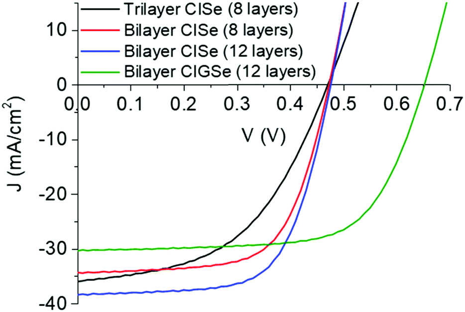 | ||
| Fig. 3 J–V characteristics of selenized CIS and CIGS film with different film morphologies. | ||
With the modification near the back contact of the film, device optimization was performed by increasing the thickness of the CIS precursor film and by introducing gallium. Performance of the devices fabricated is shown in Table 1 which highlights the improvement in efficiency through increased Jsc for a film with higher thickness and a further increase in efficiency through increased Voc for a film with the addition of gallium. The active area efficiency of 14.1% observed here for CIGSe device is the highest for amine–thiol based uniform composition CIGSe films. The application of a gallium gradient, surface treatments, OVC near interface, Ag addition, and heavy alkali treatments are known to improve the performance of CIGSe films. As most of the aforementioned strategies have already been demonstrated for amine–thiol based CIGSe films,8–11 our amine–thiol based uniform CIGSe film has more potential to improve its performance through these modifications.
Analysis of fine-grain layer
Although a promising efficiency has been achieved with amine–thiol CISe/CIGSe films by manipulating the location of the fine-grain layer, the presence of the fine-grain layer isn’t ideal and has limited the absorber thickness to a maximum of around 1.2–1.3 μm for the current highest efficiency solution processed routes. This thickness is almost half of what has been traditionally used in high efficiency vacuum based routes. To understand the cause of fine-grain layer formation in amine–thiol based films, the layer was analyzed using Raman spectroscopy. However, as this technique uses a 632.8 nm laser, it doesn’t penetrate to the back of a 1-micron thick film and hence gives a signal primarily corresponding to the top of the film which generally doesn’t have a fine-grain layer. To access the fine-grain layer for Raman spectroscopy analysis, the film was exfoliated using epoxy and then the analysis was performed from the back surface. The Raman spectrum obtained from the back of the film shows a small peak corresponding to CISe at ∼178 cm−1 which is believed to be representing the bottom of the CISe grain (Fig. 4a). However, it shows a very strong peak corresponding to amorphous selenium near 250 cm−1 and a characteristic peak corresponding to graphitic carbon in the range of 1300–1600 cm−1 suggesting a presence of C and Se in this layer (Fig. 4b).25–27 As no carbon containing species is introduced in the film during selenization, the source of graphitic carbon in the selenized film must be originating from the precursor film itself. While FTIR study of the precursor film did not show any organic carbon residue for a film annealed at a temperature of 350 °C, Raman spectra of the same precursor film confirmed the presence of graphitic carbon prior to selenization (Fig. S4, ESI†). In previous work, it was shown that copper and indium form metal thiolate species when dissolved in amine–thiol solution.28 The thiol in these thiolates serves as a sulfur source for the metal sulfide material. In this reaction when a metal sulfur bond is formed from a thiolate species, a C–S bond is broken and if both the C–S bonds break from a dithiol molecule the carbon could get converted to graphitic carbon during annealing and may not leave easily from the film. This carbon can remain in the film during selenization giving rise to a fine-grain layer and hence needs to be removed completely prior to selenization.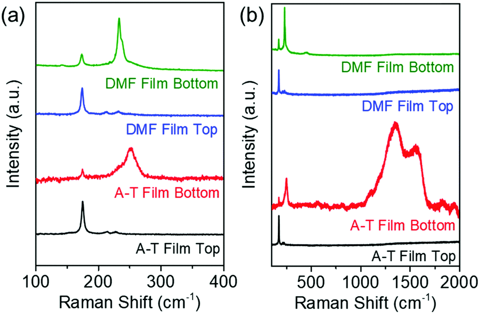 | ||
| Fig. 4 Raman spectra on selenized CIS film fabricated from amine–thiol (A–T) based route and DMF based route from both top and bottom surface of the film. (a) Raman spectra focused near CISe peaks and (b) full Raman spectra. | ||
Unlike the amine–thiol system, another route in the literature using the DMF as a solvent and thiourea as a complexing agent has demonstrated fine-grain free CISe films with an absorber thickness of up to 1.2–1.3 microns. This route has claimed to create a carbon-free film which could be a reason for its success in creating fine-grain free films.29 However, despite the ability to create carbon-free films, the DMF–TU route hasn’t reported any absorber above 1.3 μm thickness suggesting the possibility of some additional challenges besides carbon in creating a thicker absorber. To investigate this, two CIS films, one with 1-micron thickness and the other with 2-micron thickness were fabricated using a DMF–TU based route and selenized in a tube furnace. Consistent with reports in the literature, the 1-micron thick DMF–TU film indeed formed a fine-grain free morphology (Fig. 5a). However, the 2-micron thick DMF–TU film showed the formation of a secondary fine structured layer at the bottom of the selenized film (Fig. 5b). When analyzed under Raman spectroscopy after exfoliation, this layer showed a strong Se peak corresponding to trigonal selenium at around 234 cm−1 instead of amorphous selenium25 as was observed in the case of the amine–thiol film (Fig. 4a). As both DMF and TU chemicals do not have any C–C bond, a clean spectrum near the graphitic carbon region was expected to be seen. However, the fact that Se was retained in the film despite the high processing temperature during selenization, suggests the possible coordination of Se with some undesired species in the solution and the formation of a secondary layer in thicker films.
 | ||
| Fig. 5 Cross-section SEM images of (a) 1 μm and (b) 2 μm thick CISe film fabricated by selenization of a DMF based CIS film showing the presence of a fine-grain layer in the case of a 2 μm thick film. | ||
Additionally, when a 2 μm thick DMF–TU film was analyzed under SEM-EDS at different spots, it was observed that the bottom of the film (fine-grain region) and the top of the film had different Cu/In and Se/cation ratios suggesting nonuniformity of the elemental distribution in the final film (Fig. S5, ESI†). This was also evident from the STEM-EDS elemental mapping performed on thin lamella obtained from a selenized amine–thiol CIS film using a focused ion beam (FIB) technique. This mapping shows the presence of Se, C, and Cu with the absence of indium in the fine-grain layer (Fig. 6) which is consistent with previous reports on elemental mapping of CIGSe films, confirming the non-uniformity in elemental distribution across the film thickness.30,31
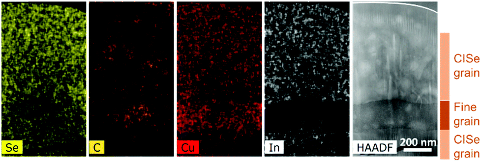 | ||
| Fig. 6 STEM-EDS elemental mapping of thin lamella obtained from the selenized CIS film showing elemental non-uniformities between grain and fine-grain layer in the film. | ||
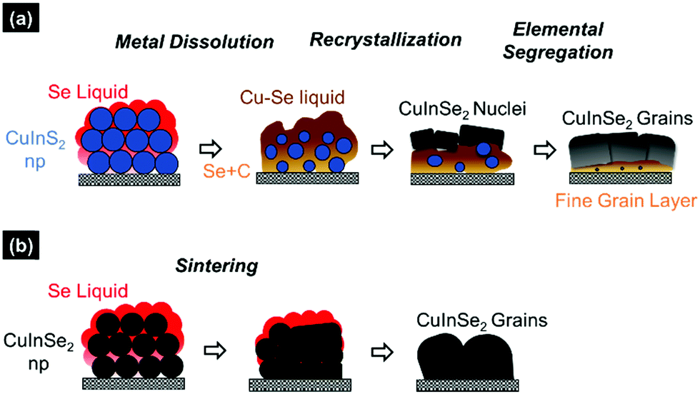
The mechanism that is responsible for creating metal non-uniformity and segregating Se-rich material at the bottom of the film could be associated with the process of selenization. Reports in the literature have shown that the process of sulfide to selenide conversion in the case of a CZTS film, or even pure metal to metal selenide in the case of the CIGS film proceeds through the formation of a Cu–Se rich liquid phase which starts nucleating copper selenide material.32–35 The remaining cations then start diffusing towards these nuclei making the desired ternary or quaternary selenide materials in the form of grains on the surface of the film that continues to grow towards the bottom (Fig. 7a). In this process, especially when the film exceeds a certain thickness, the rate of mass transfer and the reaction rates between copper and indium chalcogenides could affect the elemental distributions and hence the grain growth in the film.30,31,36 Based on these results, it is hypothesized that to enable thick film fabrication of the CISe/CIGSe absorber, free of any phase/elemental non-uniformities, the precursor film should meet the following two criteria before selenization; (1) the precursor film should be a selenide film instead of a sulfide film which will avoid dissolution of Cu in Se liquid allowing for a bulk sintering growth mechanism which should result in uniform elemental distribution throughout the film and (2) the precursor film should be free of any contamination like carbon to avoid segregation of those contaminants in the form of a fine-grain layer. To meet these criteria, Se addition to the precursor film is required and unlike other solution routes it can be achieved using amine–thiol solvents.
 | ||
| Fig. 7 Schematic representation of the CISe grain growth mechanism during selenization for the (a) CIS precursor film and (b) CISe precursor film. | ||
Se addition in the precursor film
The amine–thiol solvent system can dissolve Se along with metal precursors and such solutions have been used in past for the synthesis of CISSe nanoparticles with different compositions of S and Se.37 Similar solutions were prepared by dissolving Cu2S and In in BA-EDT solution and adding different quantities of elemental Se. Increasing amount of Se in the ink resulted in more CISe formation in the precursor film (Fig. S6, ESI†). However, despite using an Se/In ratio of 4 in the ink (100% excess Se), the precursor film yielded Se/In ratio of only 1.8 along with extremely porous film which can be associated with the evaporation of excess Se during annealing (Fig. S7, ESI†).It has been shown in previous studies that Se in amine–thiol solution forms polyselenide species which consist of multiple Se atoms sharing a common negative charge.38 This implies that very few Se atoms are completely reduced while most are still present in the elemental form lowering the overall reactivity of Se with metal cations. So, to increase the Se incorporation in the film, one needs to increase the quantity of completely reduced Se species (Se anions) in the solution. This was achieved by creating metal selenide ink with Cu2Se and In2Se3 that was prepared in BA-EDT solution without any addition of elemental Se (overall Se/In ratio in ink = 2) and a precursor film was then fabricated by annealing at 300 °C. This film yielded a Se/In ratio of 1.8 which is higher than the Se/In ratio of 1.4 that was obtained for the film fabricated from an ink containing Cu2S, In and elemental Se having an identical Se/In ratio of 2 in the ink. This result emphasizes the importance of the nature of Se species in the solution and supports the hypothesis that having more Se anions yields higher Se incorporation in the precursor film. To further increase the Se incorporation, 100% excess Se was added to metal selenide ink and a precursor film without any distinct porosity was fabricated. This film showed an Se/In ratio of 2.6 with a residual presence of CIS from XRF and Raman spectroscopy (Fig. 8). Once the desired elemental composition of the precursor film was achieved from the metal selenide precursors, the presence of carbon was also analyzed using Raman spectroscopy. As discussed earlier, the breaking of C–S bond in thiol leads to the formation of graphitic carbon in the film. So, the presence of Se anions can replace the thiolate and form metal selenide bonds which would result in cleaving the metal–S bonds in the thiolate and allow for easy removal of thiol by simple evaporation (Scheme S1, ESI†). This mechanism is supported by Raman data which shows a decrease in graphitic carbon peak in the precursor film having a higher selenium concentration (Fig. 8). The correlation between Se and C, i.e. more selenide material leads to lower carbon is further validated by Raman spectra collected on precursor films fabricated at different temperatures (Fig. S8, ESI†) and from various ink combinations of Cu, Cu2S, In, Cu2Se, In2Se3, and Se (Fig. S9, ESI†). Along with graphitic carbon, the CISe ink prepared from selenide precursors and elemental selenium also showed removal of organic carbon at temperatures as low as 250 °C which is around 100 °C lower than what was needed for the sulfide precursor film, further confirming the importance of Se anion on the removal of organic residue from the film (Fig. S10, ESI†). This film when annealed at 300 °C showed XRF and Raman spectra identical to those of the hydrazine based CISSe precursor film implying the formation of superior quality precursor film from a non-hydrazine solution route (Fig. S11, ESI†).
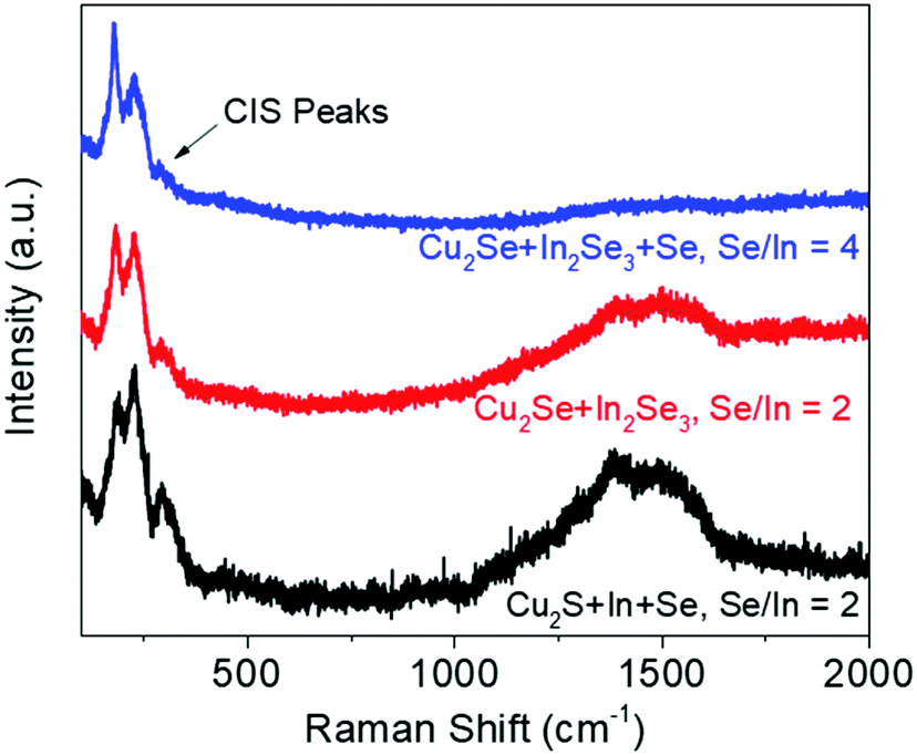 | ||
| Fig. 8 Raman spectra of precursor films fabricated with different inks showing reduction in the CIS peak and the carbon peak with increasing selenium anion quantity in the solution. | ||
Annealing optimization
With the successful fabrication of the selenide precursor film largely free of detectable impurities, the difference in the growth mechanism for CIS and CISe precursor films fabricated directly on a Mo coated glass substrate was studied by performing a time study during the process of selenization. Both CIS and CISe films were treated with selenium pellets at a temperature of 500 °C for 2 min, 4 min, and 6 min, in a graphite box which was immediately pulled out of the heating zone and allowed to cool down to room temperature. These samples were then analyzed by SEM, XRD, and Raman. The XRD and Raman spectra show a transition of the CIS material to CISe material and show the formation of larger crystalline domains for both CIS and CISe samples for even the processing time of as low as 2 min (Fig. S12, ESI†). SEM on the other hand reveals more differences in the growth mechanism (Fig. 9). As expected, the CIS film shows the formation of grains on the surface of the film at 2 min which is followed by the formation of grains at the back Mo surface (no MoO3 was used in this sample) forming an unsintered fine-grain-like layer in the middle. After 6 min both grain layers continue to grow while maintaining the trilayer morphology. This growth is also observed from top-view SEM images of these films where the average grain size shows an increase with time (Fig. S13, ESI†). On the other hand, the CISe precursor film does not show any preferential grain growth on any surface. As previously hypothesized, the film undergoes bulk sintering where the grains keep growing throughout the thickness of the film irrespective of the location. Because of such bulk sintering, the top-view SEM images don’t show a drastic change in the grain sizes as a function of time.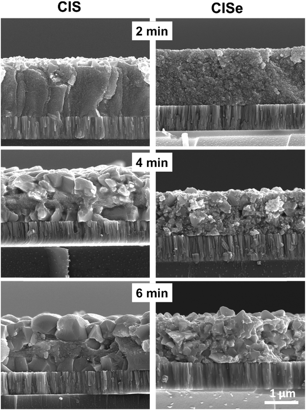 | ||
| Fig. 9 Cross-section SEM images of selenized CIS and CISe precursor films for different time intervals. | ||
The modified growth mechanism of surface-independent bulk growth provides a route for growing uniform absorbers irrespective of their thickness. To investigate the thickness independence on film growth, two precursor films were fabricated using CISe precursor inks with a total of 6 layers and 12 layers. These films were then selenized in a tube furnace and analyzed under a SEM. As can be seen from the images in Fig. 10a and b, both films showed a fine-grain free morphology making the 12 layer film the first-ever reported 2-micron thick fine-grain free film from any hydrazine-free solution processing routes with a uniform grain morphology throughout the film thickness. Similar to the CISe film, selenization of gallium containing CIGSe precursor films also create fine-grain free morphologies for certain elemental compositions (Fig. 10c). While selenization of CISe precursor films yield significant grain growth, due to the presence of excess Se in the precursor film, even an inert atmospheric annealing (nitrogen/argon without Se vapors) of these films produces large grains with extremely flat surface morphology (Fig. 10d). This morphology is very similar to the ones reported in the literature for hydrazine-based films as well as vacuum-based films and have great potential for large-scale manufacturing due to a simple high-temperature inert atmosphere annealing procedure.
 | ||
| Fig. 10 Cross-sectional SEM images of (a) ∼1 μm thick and (b) ∼2 μm thick selenized CISe precursor films, (c) ∼2 μm thick selenized CIGSe precursor film (Ga/Ga + In = 0.1), and (d) ∼2 μm thick 540 °C annealed CISe precursor film. | ||
Despite the promising film morphology, the optoelectronic properties of the new CISe film are poor compared to a device fabricated from CIS precursor film. The power conversion efficiency observed for this film was only around 3.04%, with Jsc, Voc, and FF of around 20.2 mA cm−2, 310 mV, and 48.5% respectively. Comparing the J–V data for this device with a device fabricated from the CIS precursor film suggests similar dark shunting behavior in both cases (Fig. 11a). However, the new CISe device shows a unique light shunting characteristic in reverse bias. It also shows crossover at a much lower voltage which has been previously correlated with defect formation near the CdS interface.39 Along with J–V data, the photoluminescence of the new CISe material shows almost an order of magnitude lower signal compared to that of the traditionally grown CISe film from the sulfide precursor (Fig. 11b). These results suggest the possible formation of defects in the bulk and/or near the interface of the newly grown material (also see Fig. S14, ESI†). Few plausible causes for the formation of defects in these new films could be as follows: (1) Due to the bulk sintering of the film, any residual carbon impurity which is not getting detected by Raman spectroscopy might be getting trapped between grains instead of getting pushed at the back of the film. This could affect the electron–hole recombination and lower the performance. (2) Due to the absence of any copper–selenium liquid which is generally responsible for grain growth at higher temperatures, the bulk sintering might be causing the formation of multiple crystal domains leading to multiple grain boundaries in the bulk of a microstructure grain observed in SEM. (3) Due to the selenide precursor film, the selenium wetting on the surface at the start of selenization and also during the cooling of the film could be different which could cause different defect concentration profiles in the film. Along with these, one could also correlate the poor device performance to the newly developed selenide precursor inks and the quality of precursor films themselves. However, devices fabricated from hydrazine based precursor films under similar selenization conditions also produced poor performance when replicated for this work, which suggests a possible issue with the high temperature annealing step (Fig. S15, ESI†). As the previous literature on hydrazine based films has highlighted the importance of annealing steps on the device performance and has demonstrated a much higher performance with detailed optimization; similar work is required with these new hydrazine-free CISe precursor films, to realize high efficiency devices.39 Techniques like KPFM, CV, Admittance, PL, TRPL, JVT are crucial in further investigation of defect behavior in these films.
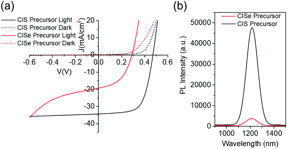 | ||
| Fig. 11 (a) J–V data and (b) PL data on selenized CIS and CISe precursor films. | ||
Conclusions
In conclusion, we showed an impact of the fine-grain layer on the performance of CISe/CIGSe devices. By manipulating the location of the fine-grain layer in the film structure through deposition of a thin MoO3 layer, CISe and CIGSe device efficiencies of 12.9% and 14.1% were achieved for uniform composition films respectively. Analysis performed on the fine-grain layer suggested Se and carbon as the primary content along with some other cations with non-uniform distributions. Similar to the amine–thiol solution route, even the DMF–TU based route showed the formation of a Se rich fine-grain layer for thicker films which suggested selenization of the CIS precursor film as a possible cause for fine-grain layer formation. By adding Se in amine–thiol based inks, the reduction of sulfide content, as well as carbon content, was observed which was then optimized by replacing metal and metal sulfides with metal selenides to achieve the complete absence of detectable carbon from the film and achieve precursor films identical to high efficiency hydrazine based films reported in the literature. With a modified precursor film from the sulfide to the selenide material, the growth mechanism was changed to bulk growth resulting in a fine-grain free film with thickness as high as 2-microns. Due to the presence of excess selenium in the precursor film, grain growth in the absence of vapor phase selenium was also demonstrated by simply annealing the film in an inert atmosphere at higher temperatures which resulted in grain growth with the added benefit of a particularly flat surface. While the grain growth modification indeed resulted in film morphologies similar to hydrazine based films, further high temperature annealing optimization along with defect characterization is required to obtain low defect and high performing CISe/CIGSe films.Conflicts of interest
There are no conflicts to declare.Acknowledgements
The authors would like to acknowledge the funding support provided by the National Science Foundation under Grants 1534691-DMR (DMREF), 1735282-NRT (SFEWS), and 1855882 (INFEWS). The research was carried out in part at the Center for Functional Nanomaterials, Brookhaven National Laboratory, which is supported by the US Department of Energy, Office of Basic Energy Sciences, under Contract No. DE-SC0012704.References
- M. Nakamura, K. Yamaguchi, Y. Kimoto, Y. Yasaki, T. Kato and H. Sugimoto Cd-free Cu(In,Ga)(Se,S)2 thin-film solar cell with a new world record efficacy of 23.35%. in 46th IEEE PVSC (2019).
- T. M. Friedlmeier, P. Jackson, A. Bauer, D. Hariskos, O. Kiowski, R. Menner, R. Wuerz and M. Powalla, High-efficiency Cu(In,Ga)Se2 solar cells, Thin Solid Films, 2017, 633, 13–17 CrossRef CAS
.
- T. D. Lee and A. U. Ebong, A review of thin film solar cell technologies and challenges, Renewable Sustainable Energy Rev., 2017, 70, 1286–1297 CrossRef CAS
- T. Zhang, Y. Yang, D. Liu, S. C. Tse, W. Cao, Z. Feng, S. Chen and L. Qian, High efficiency solution-processed thin-film Cu(In,Ga)(Se,S)2 solar cells, Energy Environ. Sci., 2016, 9, 3674–3681 RSC
- Q. Guo, G. M. Ford, H. W. Hillhouse and R. Agrawal, Sulfide Nanocrystal Inks for Dense Cu(In1−xGax)(S1−ySey)2 Absorber Films and Their Photovoltaic Performance, Nano Lett., 2009, 9, 3060–3065 CrossRef CAS PubMed
- D. B. Mitzi, M. Yuan, W. Liu, A. J. Kellock, S. Jay Chey, V. Deline and A. G. Schrott, A high-efficiency solution-deposited thin-film photovoltaic device, Adv. Mater., 2008, 20, 3657–3662 CrossRef CAS
- S. Suresh and A. R. Uhl, Present Status of Solution-Processing Routes for Cu(In,Ga)(S,Se)2 Solar Cell Absorbers, Adv. Energy Mater., 2021, 11, 2003743 CrossRef CAS
- Y. Zhao, S. Yuan, Q. Chang, Z. Zhou, D. Kou, W. Zhou, Y. Qi and S. Wu, Controllable Formation of Ordered Vacancy Compound for High Efficiency Solution Processed Cu(In,Ga)Se2 Solar Cells, Adv. Funct. Mater., 2020, 31, 2007928 CrossRef
- Q. Fan, Q. Tian, H. Wang, F. Zhao, J. Kong and S. Wu, Regulating the starting location of front-gradient enabled highly efficient Cu(In,Ga)Se2 solar cells via a facile thiol–amine solution approach, J. Mater. Chem. A, 2018, 6, 4095–4101 RSC
- Y. Zhao, S. Yuan, D. Kou, Z. Zhou, X. Wang, H. Xiao, Y. Deng, C. Cui, Q. Chang and S. Wu, High Efficiency CIGS Solar Cells by Bulk Defect Passivation through Ag Substituting Strategy, ACS Appl. Mater. Interfaces, 2020, 12, 12717–12726 CrossRef CAS PubMed
- S. Yuan, X. Wang, Y. Zhao, Q. Chang, Z. Xu, J. Kong and S. Wu, Solution Processed Cu(In,Ga)(S,Se)2 Solar Cells with 15.25% Efficiency by Surface Sulfurization, ACS Appl. Energy Mater., 2020, 3, 6785–6792 CrossRef CAS
- S. M. McLeod, C. J. Hages, N. J. Carter and R. Agrawal, Synthesis and characterization of 15% efficient CIGSSe solar cells from nanoparticle inks, Prog. Photovolt: Res. Appl., 2015, 23, 1550–1556 CrossRef CAS
- G. S. Park, V. B. Chu, B. W. Kim, D. W. Kim, H. S. Oh, Y. J. Hwang and B. K. Min, Achieving 14.4% Alcohol-Based Solution-Processed Cu(In,Ga)(S,Se)2 Thin Film Solar Cell through Interface Engineering, ACS Appl. Mater. Interfaces, 2018, 10, 9894–9899 CrossRef CAS PubMed
- A. R. Uhl, J. K. Katahara and H. W. Hillhouse, Molecular-ink route to 13.0% efficient low-bandgap CuIn(S,Se)2 and 14.7% efficient Cu(In,Ga)(S,Se)2 solar cells, Energy Environ. Sci., 2016, 9, 130–134 RSC
- J. Jiang, R. Giridharagopal, E. Jedlicka, K. Sun, S. Yu, S. Wu, Y. Gong, W. Yan, D. S. Ginger, M. A. Green, X. Hao, W. Huang and H. Xin, Highly efficient copper-rich chalcopyrite solar cells from DMF molecular solution, Nano Energy, 2020, 69, 104438 CrossRef CAS
- Q. Guo, G. M. Ford, R. Agrawal and H. W. Hillhouse, Ink formulation and low-temperature incorporation of sodium to yield 12% efficient Cu(In,Ga)(S,Se)2 solar cells from sulfide nanocrystal inks, Prog. Photovolt: Res. Appl., 2013, 21, 64–71 CrossRef CAS
- R. G. Ellis, J. W. Turnley, D. J. Rokke, J. P. Fields, E. H. Alruqobah, S. D. Deshmukh, K. Kisslinger and R. Agrawal, Hybrid Ligand Exchange of Cu(In,Ga)S2 Nanoparticles for Carbon Impurity Removal in Solution-Processed Photovoltaics, Chem. Mater., 2020, 32, 5091–5103 CrossRef CAS
- D. Zhao, Q. Fan, Q. Tian, Z. Zhou, Y.-N. Meng, D.-X. Kou, W.-H. Zhou and S. Wu, Eliminating fine-grained layers in Cu(In,Ga)(S,Se)2 thin films for solution-processed high efficiency solar cells, J. Mater. Chem. A, 2016, 4, 13476–13481 RSC
- X. Zhao, M. Lu, M. J. Koeper and R. Agrawal, Solution-processed sulfur depleted Cu(In,Ga)Se2 solar cells synthesized from a monoamine–dithiol solvent mixture, J. Mater. Chem. A, 2016, 4, 7390–7397 RSC
- Q. Yu, J. Shi, L. Guo, B. Duan, Y. Luo, H. Wu, D. Li and Q. Meng, Eliminating multi-layer crystallization of Cu2ZnSn(S,Se)4 absorber by controlling back interface reaction, Nano Energy, 2020, 76, 105042 CrossRef CAS
- S. Ranjbar, G. Brammertz, B. Vermang, A. Hadipour, S. Cong, K. Suganuma, T. Schnabel, M. Meuris, A. F. da Cunha and J. Poortmans, Improvement of kesterite solar cell performance by solution synthesized MoO3 interfacial layer, Phys. Status Solidi A, 2017, 214, 1–6 CrossRef
- L. Liu, T. K. Lau, Z. Zhi, L. Huang, S. Wang and X. Xiao, Modification of Mo Back Contact with MoO3−x Layer and its Effect to Enhance the Performance of Cu2ZnSnS4 Solar Cells, Sol. RRL, 2018, 2, 1–10 Search PubMed
- T. Schnabel and E. Ahlswede, On the interface between kesterite absorber and Mo back contact and its impact on solution-processed thin-film solar cells, Sol. Energy Mater. Sol. Cells, 2017, 159, 290–295 CrossRef CAS
- Z. He, Y. Liu, S. Lin, S. Shi, S. Sun, J. Pang, Z. Zhou, Y. Sun and W. Liu, Energy Band Alignment in Molybdenum Oxide/Cu(In,Ga)Se2 Interface for High-Efficiency Ultrathin Cu(In,Ga)Se2 Solar Cells from Low-Temperature Growth, ACS Appl. Energy Mater., 2020, 3, 3408–3414 CrossRef CAS
- G. Lucovsky, A. Mooradian, W. Taylor, G. B. Wright and R. C. Keezer, Identification of the Fundamental Vibrational Modes Of Trigonal, Monoclinic and Amorphous Selenium, Solid State Commun., 1967, 5, 113–117 CrossRef CAS
- F. Tuinstra and J. L. Koenig, Raman Spectrum of Graphite, J. Chem. Phys., 1970, 53, 1126–1130 CrossRef CAS
- L. G. Caņado, K. Takai, T. Enoki, M. Endo, Y. A. Kim, H. Mizusaki, A. Jorio, L. N. Coelho, R. Magalhães-Paniago and M. A. Pimenta, General equation for the determination of the crystallite size la of nanographite by Raman spectroscopy, Appl. Phys. Lett., 2006, 88, 1–4 Search PubMed
- X. Zhao, S. D. Deshmukh, D. J. Rokke, G. Zhang, Z. Wu, J. T. Miller and R. Agrawal, Investigating Chemistry of Metal Dissolution in Amine–Thiol Mixtures and Exploiting It toward Benign Ink Formulation for Metal Chalcogenide Thin Films, Chem. Mater., 2019, 31, 5674–5682 CrossRef CAS
- A. R. Uhl, A. Rajagopal, J. A. Clark, A. Murray, T. Feurer, S. Buecheler, A. K. Y. Jen and H. W. Hillhouse, Solution-Processed Low-Bandgap CuIn(S,Se)2 Absorbers for High-Efficiency Single-Junction and Monolithic Chalcopyrite-Perovskite Tandem Solar Cells, Adv. Energy Mater., 2018, 8, 1–8 Search PubMed
- S. Rehan, K. Y. Kim, J. Han, Y. J. Eo, J. Gwak, S. K. Ahn, J. H. Yun, K. H. Yoon, A. Cho and S. J. Ahn, Carbon-Impurity Affected Depth Elemental Distribution in Solution-Processed Inorganic Thin Films for Solar Cell Application, ACS Appl. Mater. Interfaces, 2016, 8, 5261–5272 CrossRef CAS PubMed
- A. R. Uhl, P. Fuchs, A. Rieger, F. Pianezzi, C. M. Sutter-Fella, L. Kranz, D. Keller, H. Hagendorfer, Y. E. Romanyuk, F. LaMattina, S. Yoon, L. Karvonen, T. Magorian-Friedlmeier, E. Ahlswede, D. VanGenechten, F. Stassin and A. N. Tiwari, Liquid-selenium-enhanced grain growth of nanoparticle precursor layers for CuInSe 2 solar cell absorbers, Prog. Photovolt: Res. Appl., 2015, 23, 1110–1119 CrossRef CAS
- C. J. Hages, M. J. Koeper, C. K. Miskin, K. W. Brew and R. Agrawal, Controlled grain growth for high performance nanoparticle-based kesterite solar cells, Chem. Mater., 2016, 28, 7703–7714 CrossRef CAS
- W. K. Kim, E. A. Payzant, S. Yoon and T. J. Anderson, In situ investigation on selenization kinetics of Cu-In precursor using time-resolved, high temperature X-ray diffraction, J. Cryst. Growth, 2006, 294, 231–235 CrossRef CAS
- R. Mainz, B. C. Walker, S. S. Schmidt, O. Zander, A. Weber, H. Rodriguez-Alvarez, J. Just, M. Klaus, R. Agrawal and T. Unold, Real-time observation of Cu2ZnSn(S,Se)4 solar cell absorber layer formation from nanoparticle precursors, Phys. Chem. Chem. Phys., 2013, 15, 18281–18289 RSC
- N. J. Carter, R. Mainz, B. C. Walker, C. J. Hages, J. Just, M. Klaus, S. S. Schmidt, A. Weber, W. C. D. Yang, O. Zander, E. A. Stach, T. Unold and R. Agrawal, The role of interparticle heterogeneities in the selenization pathway of Cu–Zn–Sn–S nanoparticle thin films: a real-time study, J. Mater. Chem. C, 2015, 3, 7128–7134 RSC
- S. Ahn, Y. J. Choi, K. Kim, Y. J. Eo, A. Cho, J. Gwak, J. H. Yun, K. Shin, S. K. Ahn and K. Yoon, Amorphous Cu-In-S nanoparticles as precursors for CuInSe2 thin-film solar cells with a high efficiency, ChemSusChem, 2013, 6, 1282–1287 CrossRef CAS PubMed
- S. D. Deshmukh, R. G. Ellis, D. S. Sutandar, D. J. Rokke and R. Agrawal, Versatile Colloidal Syntheses of Metal Chalcogenide Nanoparticles from Elemental Precursors Using Amine-Thiol Chemistry, Chem. Mater., 2019, 31, 9087–9097 CrossRef CAS
- S. D. Deshmukh, L. F. Easterling, J. M. Manheim, N. J. LiBretto, K. G. Weideman, J. T. Miller, H. I. Kenttämaa and R. Agrawal, Analyzing and Tuning the Chalcogen–Amine–Thiol Complexes for Tailoring of Chalcogenide Syntheses, Inorg. Chem., 2020, 59, 8240–8250 CrossRef CAS PubMed
- Q. Cao, O. Gunawan, M. Copel, K. B. Reuter, S. J. Chey, V. R. Deline and D. B. Mitzi, Defects in Cu(In,Ga)Se2 chalcopyrite semiconductors: A comparative study of material properties, defect states, and photovoltaic performance, Adv. Energy Mater., 2011, 1, 845–853 CrossRef CAS
Footnote |
| † Electronic supplementary information (ESI) available. See DOI: 10.1039/d2ma00095d |
| This journal is © The Royal Society of Chemistry 2022 |