
 Open Access Article
 This Open Access Article is licensed under a Creative Commons Attribution-Non Commercial 3.0 Unported Licence
Template-free chemical deposition of highly crystalline ZnO nanorod thin films
Rajagopalan
Thiruvengadathan
 *ab,
Swati
Dhua
c,
Sanju
Rani
d,
Cherian Joseph
Mathai
b,
Mengjun
Bai†
b,
Keshab
Gangopadhyay
b and
Shubhra
Gangopadhyay
b
*ab,
Swati
Dhua
c,
Sanju
Rani
d,
Cherian Joseph
Mathai
b,
Mengjun
Bai†
b,
Keshab
Gangopadhyay
b and
Shubhra
Gangopadhyay
b
aDepartment of Electronics and Communication Engineering, Amrita School of Engineering, Coimbatore, Amrita Vishwa Vidyapeetham, India. E-mail: t_rajagopalan@cb.amrita.edu
bDepartment of Electrical Engineering and Computer Science, University of Missouri, Columbia, MO 65211, USA
cSemiconducting Oxide Materials, Nanostructures and Tailored Heterojunction (SOMNaTH) Lab, Department of Physics, Indian Institute of Technology Madras, Chennai, India 600036
dDepartment of Physics, SRM Institute of Science and Technology, Ramapuram Campus, Chennai, India 600089
First published on 9th May 2022
Abstract
A template-free solvothermal method in a mixed solvent system was employed to produce ZnO nanorods in powder and thin-film forms at temperatures as low as 90 °C. A thin seed layer of ZnO nanoparticles drop-cast on Si substrates was used in some experiments to investigate the role of the seed layer in controlling the structural properties of ZnO nanorods. The structural and the morphological properties of the as-synthesized ZnO nanorods were characterized using a multitude of tools such as an X-ray diffractometer (XRD), a transmission electron microscope (TEM), a scanning electron microscope (SEM), an energy dispersive X-ray spectrometer (EDS) and a Raman spectrometer. Optical absorption and fluorescence measurements were performed to understand the absorption and emission characteristics. The results confirm that the synthesized ZnO nanorods are highly uniform in terms of crystal structure, purity, uniformity in morphology, and stoichiometry in composition.
1. Introduction
Among various one-dimensional semiconducting nanostructures, zinc oxide (ZnO) and metal-doped ZnO continue to attract attention owing to their enormous utility in a multitude of applications such as light emission, light detection, photovoltaics, sensing, energy harvesting and photocatalysis.1–8 Both top-down and bottom-up approaches have been used in the past to synthesize ZnO nanostructures with a multitude of morphologies such as spherical nanoparticles, nanorods, nanowires and nanotubes in powder and film forms. In general, the top-down approach is employed whenever device quality nanostructured films are required, and the bottom-up approach is exploited when large-scale production of nanopowders is desirable.9 Also, the common denominator in most of the bottom-up approaches is that they all belong to the family of wet chemical synthesis. All these efforts have been focused towards obtaining ZnO nanostructures with a high degree of crystallinity, stoichiometric composition, uniform shape (morphology) and size.The wet-chemical approaches often use Zn(OH)42− or Zn(NH3)42+, implying basic conditions.10–12 Also, the synthesis of crystalline ZnO nanorod arrays deposited in thin/thick films formed with zinc salts and hexamethylenetetramine (HMT) as starting precursors has been reported. Recently, Zhou et al. reported the growth of ZnO nanorods with previously deposited ZnO nanoparticles (seeds), in solutions containing zinc salts and HMT with polyethylene glycol as the medium.10
In this work, we report a template-free solvothermal synthesis of highly crystalline ZnO nanorods with varying average diameter in the range of 20–100 nm in a neutral solution depending on the synthesis conditions. It is observed that the two-step synthesis of crystalline ZnO nanorods by homogeneous precipitation involves the use of zinc salts and urea as precursors. Zn(OH)2 or zinc carbonate hydroxide was formed during the heating of zinc salt and urea solution in the first step. In the second step, the precipitates were sintered at high temperature to produce crystalline ZnO.12 Here, the authors of this work report the synthesis of ZnO nanorods employing a solvothermal approach based on refluxing in a uniform, yet controlled environment of temperature and pH in mixed solvent medium. Most importantly, surfactants were not used to control the growth of one-dimensional structures.
While previously published literature has reported the use of zinc nitrate and urea to produce ZnO nanorods in the powder form, the authors have followed the same methodology to produce ZnO films using a seed layer of previously deposited ZnO nanoparticles. Deposition of ZnO thin films has been accomplished by a variety of physical and chemical methods including thermal evaporation,13 sputtering,14 chemical vapor deposition (CVD),15 pulsed laser deposition,16 spray pyrolysis17 electrochemical methods,18 the sol–gel method19,20 and chemical bath deposition.21 Sputtering, pulsed laser deposition, and chemical vapor deposition techniques are expensive in view of the basic requirement of specialized, vacuum-based deposition equipment. In contrast, chemical bath deposition is a simple and cost-effective process for the production of large area uniform nanostructured thin films. In this work, the authors demonstrate yet another simple technique, namely, a solvothermal refluxing method for the production of ZnO thin films.
Interestingly, the parameters affecting the nucleation and growth of films by chemical bath deposition and the solvothermal refluxing methods are very nearly alike and these include the nature and concentration of precursors, temperature, pH, substrate nature, duration and thickness and morphology of the seed layer. At the same time, the solvothermal refluxing method reported here also yields high quality and relatively large-scale nanostructured powders besides producing films. For example, the authors were able to obtain approximately 200 mg nanopowder with uniform nanorod morphology in a typical synthesis that uses about 1.78 g of Zn(NO3)2·6H2O and 1.08 g of CH4N2O. Deposition of nanostructured ZnO films using the solvothermal approach and their complete characterization has not been reported earlier to the best of the authors’ knowledge. Besides, the role of a seed layer grown using simple drop-casting of ZnO nanoparticle dispersions in controlling the growth of ZnO nanostructured films with nanorod morphology has also been investigated here. A similar study conducted to investigate the effects of seed-controlled nucleation and growth using chemical bath deposition has been reported by Suhaimi et al.21 The ZnO seed layer was grown on Si and quartz substrates by drop-casting a highly dilute and stable suspension of ZnO nanoparticles. The synthesized ZnO nanorods in both powder and film forms were characterized to study their structure, morphology, composition, optical absorption and fluorescence emission properties.
More significantly, the potential for application of ZnO nanorods, particularly in the realm of optoelectronics is enormous, as has been conspicuously noticed from the large volume of original research data published over the past two decades on this material from synthesis to application development. However, the fundamental challenge in utilizing ZnO nanorods in optoelectronic devices is that these nanorods emit light over a large range of wavelengths in the UV and visible part of the electromagnetic spectrum. This broad emission is related to defects. It is therefore desirable to develop suitable synthesis routes and optimize the process parameters so that the defect related emissions are narrow in pristine ZnO nanorods. On another note, published studies report alternate means to control the emission characteristics via coating with other materials like graphene oxide sheets22 or chromium23 (Cr), growing ZnO nanorods in a Zn-rich environment24 and so on. Interestingly, thermal annealing treatment post coating of ZnO nanorods with Cr has been reported to enable diffusion of Cr and subsequent occupation of oxygen vacancies in the ZnO lattice, leading to enhanced visible emission while simultaneously suppressing the UV emission. In this work, pristine ZnO nanorods produced through the solvothermal refluxing method at low temperatures over a long time of several hours are found to emit narrow (lower FWHM) defect-related emission in the visible part of the EM spectrum.
2. Experimental
A single-step refluxing approach was employed for the preparation of small diameter ZnO nanorods using zinc nitrate (Zn(NO3)·6H2O) (reagent grade >99.0%) and urea (CH4N2O) as reactants in a mixed solvent medium of absolute ethyl alcohol and water. In a standard procedure, 1.78 g Zn(NO3)·6H2O (analytical reagent; 99.0%) and 1.08 g CH4N2O (reagent grade: 99.0%) were mixed in a solution of absolute ethanol and deionized (DI) water with a volume ratio of 3![[thin space (1/6-em)]](https://www.rsc.org/images/entities/char_2009.gif) :7. Thus, the molar ratio of Zn(NO3)·6H2O to CH4N2O is 1:3. The viscosity of solution was found to be nearly 2 mPa s.
:7. Thus, the molar ratio of Zn(NO3)·6H2O to CH4N2O is 1:3. The viscosity of solution was found to be nearly 2 mPa s.
In a typical experiment, the pH value was set nearly to 2.0 by adding HNO3 prior to refluxing. After refluxing for varying durations from 8 to 16 h at 90 °C (using an oil bath for ensuring a uniform temperature), a white-colored precipitate was observed and collected. The white precipitates were washed with DI water and ethanol alternatively thrice using an ultrasonic bath (Cole Parmer – 40 kHz) and dried in air at ambient temperature. In order to investigate the effects of pH on the morphology of synthesized ZnO, the authors synthesized ZnO at two other pH values, 4.0 and 7.0, keeping all other above-mentioned parameters identical.
In some experiments, a thin layer of commercially purchased ZnO nanoparticles (with an average particle size of 30 nm) was deposited on well cleaned Si and quartz substrates using a solution casting method. For this purpose, dispersions of ZnO nanopowder in isopropyl alcohol (IPA) were prepared by subjecting the solution to ultrasonic treatment overnight and then centrifugation at 4000 rpm for 20 minutes was performed to separate the supernatant from settled precipitates (aggregated state). The starting concentration of ZnO was about 1 wt%. The process was repeated thrice, each time using the supernatant alone, to get well dispersed nanoparticles in IPA. Thus, the concentration of the solution was reduced due to successive centrifugations to remove the precipitates. By selectively evaporating the solvent, the concentration of the dispersions is increased such that the stability of the dispersions is not affected. The final concentration of ZnO solid content in stable dispersions was nearly 0.05 wt%. The concentrated solution was drop-cast on low doped p-type silicon and quartz substrates, and then the sample was kept in the oven with a temperature of 65 °C for 4 hours to grow the seed layer. These coated Si substrates with the seed layer of ZnO nanoparticles were then carefully placed in a round flask containing the reactant mixture of (Zn(NO3)·6H2O) and urea in a mixed solvent medium. ZnO nanorods were then grown on Si substrates with ZnO nanoparticles using the refluxing method described above and the refluxing was performed for about 16 hours.
Both, the white-colored powder and the films synthesized using the procedures described above were characterized using several analytical tools. A Rigaku X-ray diffractometer (model: Ultima IV) with Cu Kα radiation (λ = 0.15418 nm) was used to determine the sample purity and crystal structure. A Philips (FEI) EM420T transmission electron microscope (TEM) operated at 120 kV and a Hitachi S4700 cold-cathode field emission scanning electron microscope (SEM) equipped with an energy dispersive X-ray spectroscopic analyzer (EDS) were used to determine the shape, size, and distribution. Raman measurements were accomplished at room temperature using a Renishaw inVia spectrometer furnished with an argon ion laser (20 mW) excitation, at 514.5 nm. A UV-VIS spectrometer (Shimadzu make; model 2400 PC) was used to acquire absorption data in the 200–900 nm wavelength range. The thickness of the films was measured using Talystep (Taylor Hobson). Fluorescence measurements were made using a Horiba Jobin Yvon Fluoromax-2 spectrofluorometer. For the purpose of checking the usefulness of the synthesized ZnO nanorods towards UV detection application, a thin film was deposited in the following manner. About 10 mg of ZnO nanorods were dispersed in 500 microliters of ethanol, at a concentration of 2 wt%. About 20 microliters of this dispersion was drop-cast carefully on the interdigitated electrode (IDE) and left overnight for drying at room temperature. The electrode used here is identical to the one shown in a previous publication that reports a gas sensing application study.25 The photocurrent vs. time measurements were carried out by using a two probe system and Omnicure S 1000 UV-light source (320–500 nm) at different intensities. The source was previously calibrated, and the intensities were determined using a power meter.
3. Results and discussion
The X-ray diffraction patterns of ZnO nanorods formed with and without a seed layer of ZnO nanoparticles are shown in Fig. 1. All of the peaks associated with the diffraction patterns in the ZnO nanorods formed with and without any seed layer can be indexed to the hexagonal wurtzite structure of ZnO, and no impurity peaks could be observed in the ZnO film sample. Lattice constants (a, c) for ZnO nanorods with the hexagonal wurtzite structure have been calculated using the locations (2-theta) of (100) and (002) peaks in the X-ray diffraction pattern for the two samples i.e. with and without the seed layer. Our results shown in Table 1 show that the values of “a and c” are very close to the standard values reported in the literature (JCPDS 01-79-0206). The indexing of the observed peaks correlated with the reported values in the literature (JCPDS 01-79-0206). However, the shape and the intensities of the peaks with (hkl) indices (200), (112) and (201) are distinctively different for the two samples formed with and without seed layer. Since all of the synthesis parameters are the same for samples prepared with and without the seed layer, this is attributed to the influence of commercial grade ZnO nanoparticles that act as a seed layer for growth of nanorods. The diffraction pattern (not given in this paper) of the commercial grade ZnO nanopowder reveals the overlapping or convoluted nature of (200), (112) and (201) peaks.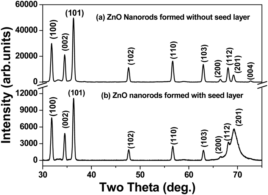 | ||
| Fig. 1 X-ray diffractogram of ZnO nanorods formed (a) without a seed layer of ZnO nanoparticles in the solution phase and (b) with a seed layer of ZnO nanoparticles pre-coated on Si substrates. Glancing angle incidence at 1° was used in the case of ZnO films on Si substrates. | ||
| Sample | Lattice parameters (Å) | Mean crystallite size (nm) | Microstrain (× 10−4) | Dislocation density (× 1015 m−2) | ||
|---|---|---|---|---|---|---|
| a | c | Debye–Scherrer | W–H plot | |||
| ZnO film without seed | 3.247 | 5.199 | 23.70 | 29.22 | 5.20 | 1.19 |
| ZnO film with seed | 3.245 | 5.196 | 27.48 | 29.76 | 2.165 | 1.12 |
The average crystallite grain size was calculated using the Debye–Scherrer's equation,
In employing this equation, the authors have considered a “uniform deformation model”, wherein the homogeneous isotropic nature of the crystal is quintessential. The authors justify the use of this model as a case of first approximation despite the hexagonal wurtzite structure of ZnO, based on the finding of the earlier work reported in the literature for ZnO nanoparticles.29 Bindu and Sabu Thomas demonstrated that the ZnO crystallite size estimated from the W–H plots using the uniform stress deformation model (USDM) and uniform deformation energy density model (UDEDM) (which considers anisotropy in the crystal structure) is nearly the same as the crystallite size obtained from the W–H plot that assumes isotropy of the crystal structure. Besides, the authors have also demonstrated that the values of crystallite size estimated for the two types of samples given in Table 1 using Debye–Scherrer and W–H plots are close to each other and within acceptable deviation between the two methods.
A scatter plot of 4sinθ along the x-axis versus βhklcosθ along the y-axis for the ZnO nanorods is first drawn using the X-ray diffraction data. From the linear fit to the scatter plot, the crystalline size can also be estimated from the y-intercept, and the strain ε, from the slope of the fit. The values of microstrain for ZnO nanorod films grown with and without a seed layer are 2.165 × 10⁻⁴ and 5.2 × 10⁻⁴ respectively. These low values of microstrain reflect the good quality of ZnO nanorod films prepared in this work. In comparison, besides the dislocation density (δ – defined as length of dislocation lines per unit volume) is determined using the following equation,
The bright field TEM micrograph (Fig. 2(a) and (b)) reveals that the synthesized ZnO material has a rod-like morphology. The sample for the TEM investigation was prepared using the dispersions of the precipitated material synthesized in the solution phase (i.e., without seed layer). While the diameter of these nanorods ranges from 20 to 100 nm, the length of these nanorods ranges from 500 nm to 1500 nm. It must be noted that the number of nanorods with larger diameter are very few in comparison to the ones formed with smaller diameter. Thus, the average diameter of these ZnO nanorods estimated using ImageJ is about 40 nm. Thus, the average aspect ratio of these nanorods is typically estimated to be 40. The growth of the nanorods was monitored in the solution phase by observing if there was any color change. The pH of the starting solution was measured to be nearly 2.0. As the reaction between urea and zinc nitrate proceeded, the pH was found to be nearly 6.5 when the transparent solution acquired a faint bluish color. At this time, the reaction was stopped, and the TEM imaging of the sample revealed the formation of floccules, along with emergence of a few ZnO nanorods (Fig. 2(a)). The solution was further refluxed under heat treatment until the pH of the solution became completely neutral. Precipitation of white colored powder occurred at this point of time and the reaction was stopped and the collected precipitates were thoroughly washed repeatedly first with deionized water and then with ethanol. The TEM micrograph of this white colored precipitate suspended in IPA taken on a carbon coated Cu grid reveals well grown crystalline ZnO nanorods (Fig. 2(b)).
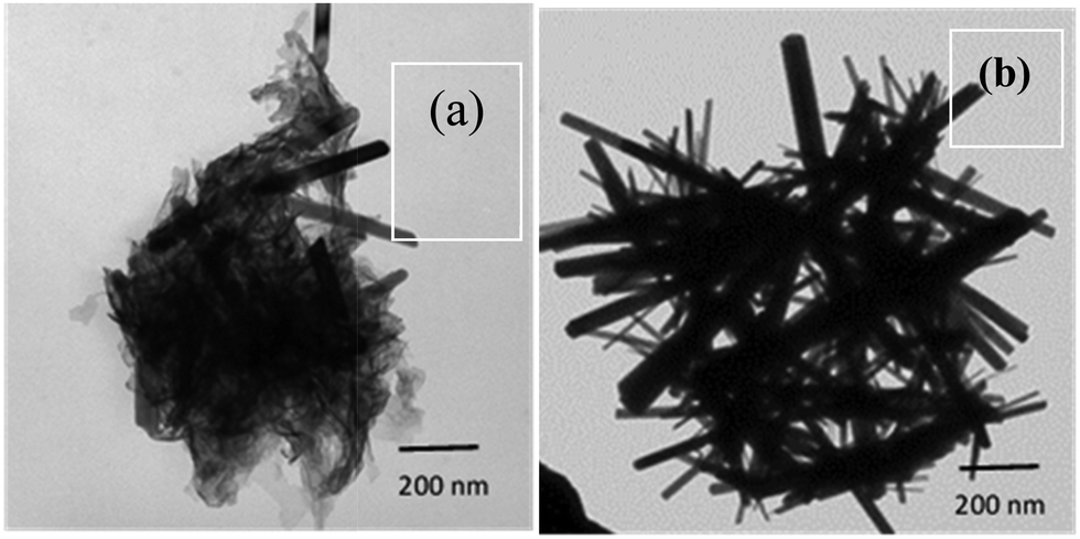 | ||
| Fig. 2 Bright field images of ZnO nanorods recorded using a 120 kV transmission electron microscope. (a) Observation of floccules, along with the emergence of a few ZnO nanorods. (b) Fully grown ZnO nanorods after the completion of solvothermal treatment under refluxing for 16 hours at 90 °C. | ||
The bright field image recorded using TEM shown in Fig. 3(a) shows the size distribution of commercial grade ZnO nanoparticles in the range of 10 to 50 nm.
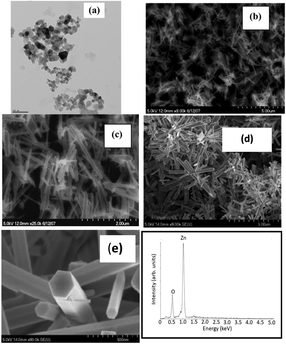 | ||
| Fig. 3 (a) TEM image of ZnO nanoparticles used as a seed layer for ZnO nanorods growth on a Si substrate with scale bar of 200 nm. (b) and (c) SEM images of ZnO nanorods grown in the solution phase without a seed layer, (d) and (e) ZnO nanorods grown on the pre-coated Si substrate with ZnO nanoparticles. (f) EDS spectrum of a ZnO nanorod sample grown on a Si substrate with the ZnO seed layer. | ||
The typical SEM images recorded at lower and higher magnification shown in Fig. 3(b) and (c) reveal the rod-like morphology of the synthesized ZnO in the solution phase. The lower magnification image shows the homogeneity of the sample. The loose powder obtained from the precipitates was dispersed and cast on a Si substrate for imaging. The diameters of these nanorods are not uniform. While the diameters of these nanorods were in the range of 20 to 100 nm, their lengths ranged from 700 nm to 1500 nm. The charging effect of these nanorods due to the incident electron beam is clearly evident from these images. The authors attribute the charging effect to the semiconducting nature of these nanorods. In contrast, the SEM images (Fig. 3(d) at lower magnification and Fig. 3(e) at higher magnification) of a ZnO film grown on a heavily doped Si substrate pre-coated with a thin layer of ZnO nanoparticles (APS of 30 nm) reveal the remarkable growth of densely packed ZnO nanorods along the c-axis with a well faceted morphology, reflecting the hexagonal crystal structure. Again, we observe a high degree of homogeneity of the sample. Both the lengths and the diameters of the nanorods grown on a Si substrate with a seed layer of ZnO nanoparticles were not only larger but their distributions were narrower in comparison to those grown in the solution phase. This implies that the seed layer of ZnO nanoparticles acted as a catalyst for the growth of ZnO nanorods, very similar to the data reported in the literature. The well faceted morphology of nanorods also suggests that each of these nanorods must be single crystalline and of high structural quality. At the same time, the fact that the authors were able to get X-ray diffraction patterns using a polycrystalline goniometer indicates that different nanorods grow with different orientations. Moreover, the X-ray diffraction patterns show several peaks (different two theta values) with significant intensity at different two-theta values. This clearly implies the polycrystalline nature of ZnO nanorods in powder and thin film form. Also, it must be noted that the commercial grade ZnO nanoparticles used as seeds are also polycrystalline in nature, implying the different orientations of crystallite grains. On the other hand, films synthesized using chemical bath deposition21 and sol–gel methods19 reported in the literature show that the intensity is particularly high for the peak (002) while the intensities of all other peaks in the diffraction pattern are relatively low. In these published reports, the nanorods exhibit a preferred direction of growth. The diameters of these nanorods were large and were in the range of 50–100 nm and the lengths were about 2000 to 2500 nm. Analysis of the EDS spectrum shown in Fig. 3(f) reveals the composition, Zn at 51.54 atom% and oxygen at 48.46 atom%. The EDS spectrum was collected at different spots along the ZnO nanorods that were grown as a thin nanostructured film on the Si substrate with the ZnO seed layer. From the analysis data, it is evident that the ZnO nanorods have a nearly stoichiometric composition.
To understand the growth of ZnO nanorods, one needs to understand the nucleation and growth stages. For the formation of 1D growth nanostructures with high areal density, the nucleation rate needs to be faster than the growth rate at the beginning, and thereafter they need to grow along the long axis (one direction only immediately. Since we observe ZnO nanorods both being produced in the solution phase as well as grown on a Si substrate pre-coated with ZnO nanoparticles, it is evident that nucleation takes place both in the solution phase and on substrates also. However, it must be noted that the ZnO nanorods grown on pre-coated Si substrates exhibit a well faceted hexagonal morphology. Our microscopic imaging studies at different magnifications confirm such a growth. At the same time, both nucleation and growth rates are expected to depend on the solubility and availability of the reacting particles. Urea is highly soluble in water, and when urea is dissolved in a mixed solvent system of ethanol to water ratio of 3:7, ammonia and carbonate anions (CO32−) are generated with the step-wise chemical reaction proceeding as follows:
| CON2H4 + 3H2O → CO2(Gas) + 2NH3·H2O |
| CO2 + 2NH3·H2O → 2NH4+ + CO32− +·OH− |
| Zn(NO3)2·6H2O + H2O → Zn2+ + 2NO3− + 7H2O |
| 4Zn2+ + CO32− + 6OH− + H2O → Zn4CO3(OH)6·H2O(s) |
Zn4CO3(OH)6·H2O(s) → 4ZnO + 4H2O + CO2 upon thermal decomposition.
The presence of ethanol in our synthesis is an important parameter to control the size of nanorods obtained as has been reported in the literature.31 Also, it is essential to keep the reactant mixture in the boiling state to enable the formation of ZnO. Otherwise, decomposition will not take place and the product will be impure with the formation of Zn5(OH)6(CO3)2 as has been reported in the literature.
Interestingly, changing the pH of the solution (from 2 to 7) did not change the morphology of ZnO formed, which is still found to be nanorod using SEM imaging though the size distributions are slightly different from each other. This observation could be possibly attributed to the formation of a zinc carbonate hydrate complex formed as an intermediate product as a result of using urea as the reactant. Moreover, the nature of the solvent (in this case a mixture of ethanol and water) is a more significant parameter in dictating the morphology. As far as precipitate formation is concerned, temperature is an important parameter as mentioned in the text for decomposition to take place, leading to ZnO formation.
Fig. 4(a) shows the Raman spectra of the ZnO nanoparticles excited by the 514.5 nm line of the Ar+ laser. The Raman spectra of both the samples, i.e., ZnO nanorods synthesized with a seed layer and ZnO nanorods synthesized without a seed layer (Fig. 4(a)) show several vibrational bands at 332, 378, 409, and 438 cm−1. Well pronounced peaks were observed in the Raman spectrum of ZnO nanorods grown on a Si substrate with the seed layer of ZnO nanoparticles. In contrast, the ZnO nanorod sample without a seed layer shows additional peaks of insignificant (weak) intensity apart from these four pronounced bands, possibly due to the presence of a very small amount of physisorbed impurities due to incomplete washing of ZnO nanorods after synthesis. The observed intense peak at 438 cm−1 is attributed to the E2 (high) Raman-active phonon mode. The peak at 332 cm−1 is attributed to the second-order phonon 2E2(M) mode. The other two peaks observed at 378 cm−1 and 409 cm−1 are attributed to A1(TO) and E1(TO) respectively. The peak assignments were based on the Raman measurements made on a single crystal of wurtzite.32 Furthermore, the published papers report the observation of the asymmetric line shape of the E2 (high) phonon at 437 cm−1 accompanied by tailing at the lower frequencies. On the other hand, the authors of this work observe that the E2 peak is nearly symmetric as seen from perfect Gaussian fits, implying the high crystalline quality of the synthesized nanorods (Fig. 4(b)). Besides, the authors do not observe shifting of this E2 peak to lower frequencies in the case of ZnO nanorods, i.e. below 437 cm−1, as has been observed for decreasing crystallite size for isotropic ZnO nanoparticles.33 ZnO nanorods synthesized in this work are of larger length and diameter as has been confirmed from electron microscopy study.
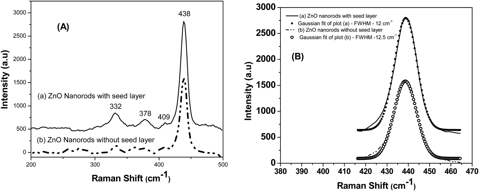 | ||
| Fig. 4 Fig. 4 (A) Raman spectra of (a) ZnO nanorods grown on the Si substrate with a seed layer and (b) ZnO nanorods grown on a Si substrate without a seed layer. (B) The Gaussian fits shown for both the samples at 416 to 464 cm−1 reveal the nearly symmetric nature of the E2 (high) phonon peak at 438 cm−1 and the slight asymmetry is seen only at low frequencies. | ||
To monitor the growth of ZnO nanorods synthesized in this work, UV-Vis absorbance measurements were performed on colloidal dispersions as a function of refluxing duration at 8 hours, 12 hours and 16 hours at an identical temperature of 90 °C (Fig. 5). The absorbance increases with increasing refluxing duration (in the measured wavelength range of 200–900 nm) under identical concentration of 0.001 wt% ZnO nanorods suspended in IPA. The appearance of a small relatively broad absorbance peak at 376 nm corresponding to a photon energy of 3.3 eV for the sample synthesized with 8 hours refluxing duration at 90 °C is indicative of the onset of the formation of ZnO nanorods. The intensity of this excitonic peak not only increases but also becomes sharper with increasing refluxing duration. There is a clear blue shift in the excitonic peak energies with increasing refluxing duration. These observations agree with the well-formed high quality ZnO nanorods for samples synthesized with 16 hours of refluxing condition, as also seen from the structural analysis performed using a host of experimental tools described earlier. The absorption coefficient in the range of 104–105 cm−1 in the visible region of the spectrum was determined, illustrating the semiconducting nature as expected.
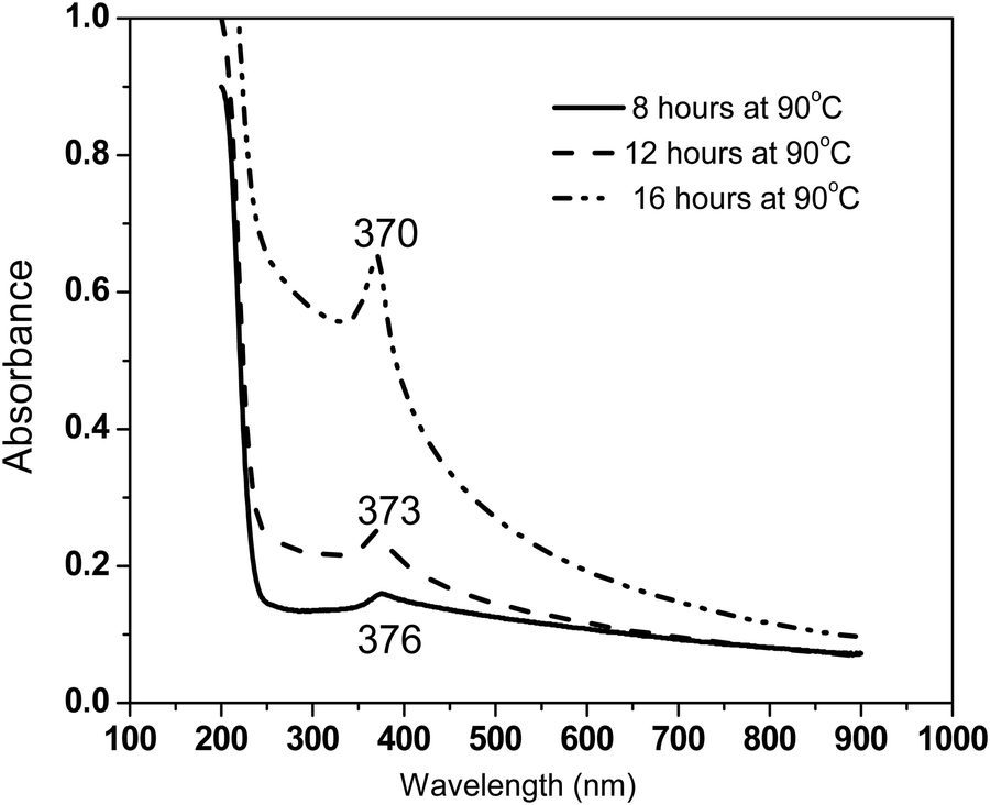 | ||
| Fig. 5 Optical absorbance of colloidal dispersions of ZnO nanorods dispersed in DI water showing the appearance of a distinct excitonic peak as a function of refluxing duration during the solvothermal synthesis process. | ||
From the Tauc plots shown for ZnO nanorod aqueous dispersions, the band gap (Eg) values were estimated using the linear fits shown in Fig. 6(a). For the optical absorbance measurements as well as fluorescence measurements in aqueous medium, the following procedure was adopted to prepare dispersions. Firstly, ZnO nanorods were carefully removed from ZnO nanorod films deposited with and without seed nanoparticles on substrates. Secondly, the ZnO nanorods in powder form were dispersed in DI water using an ultrasonic bath for 20 minutes prior to absorbance measurements. The Eg values for these dispersions shown in Fig. 6(a) are 3.35 eV and 3.4 eV with and without seed nanoparticles. The Eg values estimated using the direct band gap relation and the corresponding Tauc's plots for ZnO nanorod films with and without seed particles are 3.30 eV and 3.37 eV (Fig. 6(b)) respectively, following the same trend of Eg values determined for ZnO nanorod aqueous dispersions (Fig. 6(a)). The slight increase in the Eg value for ZnO films prepared without the seed layer in comparison to that of films with the seed layer agrees with the reduced crystallite size of 23.7 nm in comparison to that of 27.48 nm (for ZnO films prepared with ZnO seed nanoparticles) calculated using the Debye–Scherrer formula. Thus, the band gap values for ZnO nanorods both in film and powder form are nearly the same as expected. While the Eg value for ZnO nanorods without seed aqueous dispersions was found to be 3.4 eV, the Eg value for the ZnO nanorod film without the seed layer was 3.37 eV. The observed values match with reported values in correlation with calculated values of crystallite size from X-ray diffractograms.
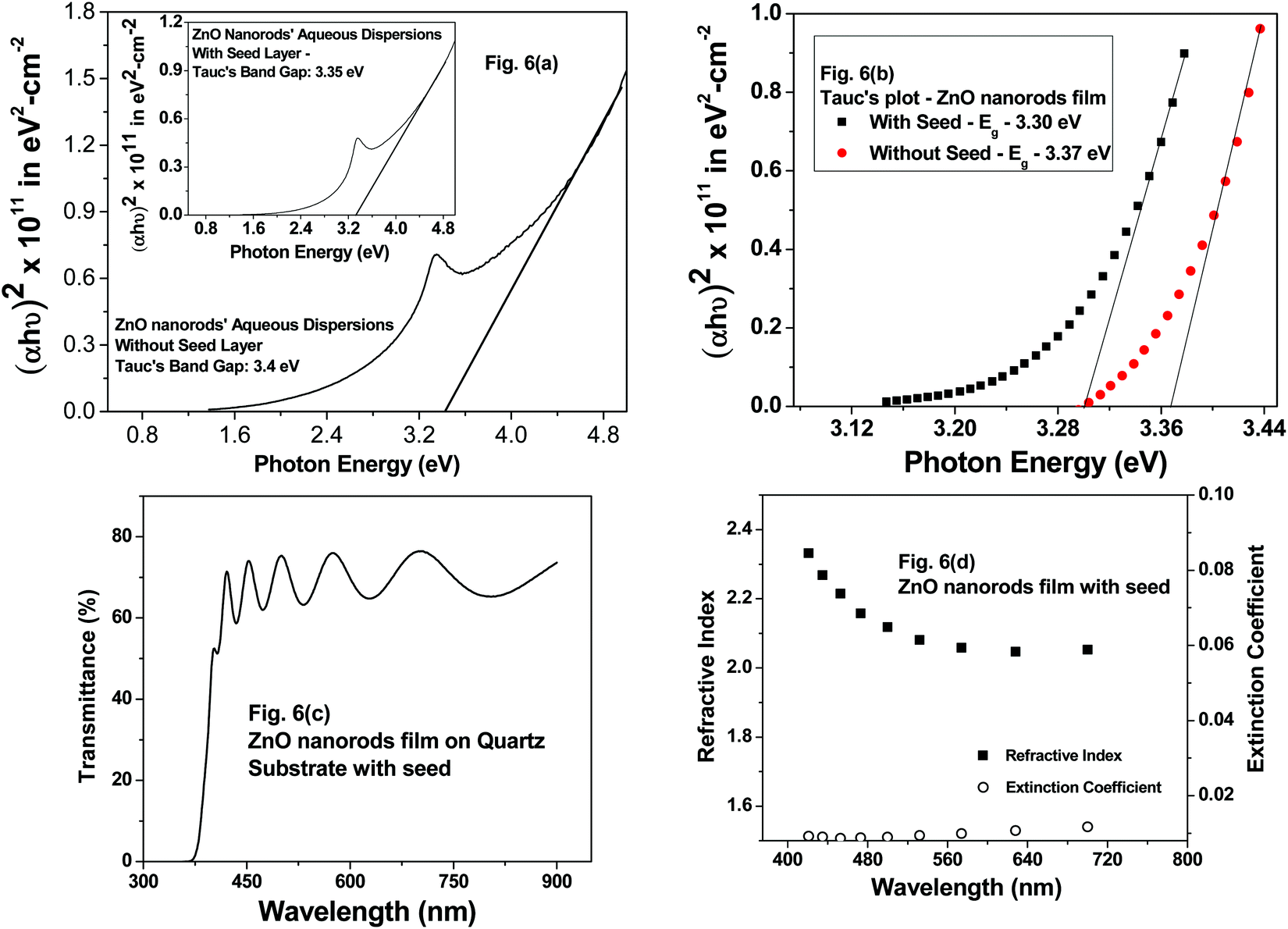 | ||
| Fig. 6 Tauc's plots to estimate the band gap of ZnO nanorods with and without seed nanoparticles in (a) aqueous dispersions and (b) ZnO nanorod films. (c) Transmittance spectrum and (d) optical constants of ZnO nanorod films with seed ZnO nanoparticles. | ||
On another related note, transmittance measurements were made on ZnO nanorod films deposited on a quartz substrate prepared with seed nanoparticles only. The transmittance spectra of ZnO nanorod films prepared with seed nanoparticles and without seed nanoparticles were nearly identical. This is not surprising, given the fact that the structural properties and the optical band gap values estimated from Tauc's plots discussed above via absorbance measurements made on samples prepared with and without a seed layer were almost the same. The authors therefore analyzed the refractive index and the extinction coefficient of ZnO nanorod films prepared with a seed layer. From the transmittance spectrum shown in Fig. 6(c), it is evident that the ZnO nanorod film interference fringes are observed. Refractive index and extinction coefficients were determined by employing the “envelope method”.34,35 Refractive index (n) values show a decreasing trend with increasing wavelength (Fig. 6(d)) and are in the range of 2.1 to 2.4, which is reflective of the semiconducting nature of ZnO nanorod films. The extinction coefficient (k) is in the range of 0.007 to 0.01 in the optical range, revealing the highly transparent nature of these films. The range of values obtained in this work match well with the reported values in the literature for ZnO nanorods, and the published work also reveals the decreasing trend in n-values.36
The fluorescence spectra of aqueous dispersions of ZnO nanorods with and without a seed layer were measured using a fluorescence spectrophotometer. Spectra were collected utilizing a 1 cm path quartz cell in the range of 390–550 nm. The excitation wavelength was 380 nm, given the band gap of 3.30–3.40 eV for different samples synthesized here. Fig. 7 shows the fluorescence spectrum of ZnO nanorods (with and without seed nanoparticles) dispersed in DI water. The fluorescence spectra of ZnO films prepared with and without nanoparticle seed layers are nearly identical to each other, in correlation with structural properties such as crystallite size, microstrain and dislocation density and optical absorption and band gap values. We have also noted that the fluorescence spectra of ZnO films prepared with and without a nanoparticle seed layer are nearly identical to each other. In the case of a sample without a seed, the spectrum exhibits a characteristic emission peak at 457 nm for pure ZnO nanorods. It is evident that this peak has an asymmetric shape. Deconvolution shows two peaks at 452 nm and 472 nm respectively. These two peaks at 452 nm and 472 nm corresponding to blue emission and the bluish green emission are assigned to zinc-related defect levels as reported in the literature. Interested readers are referred to excellent articles to understand the origin of blue emission in ZnO nanostructures due to these defects.37,38
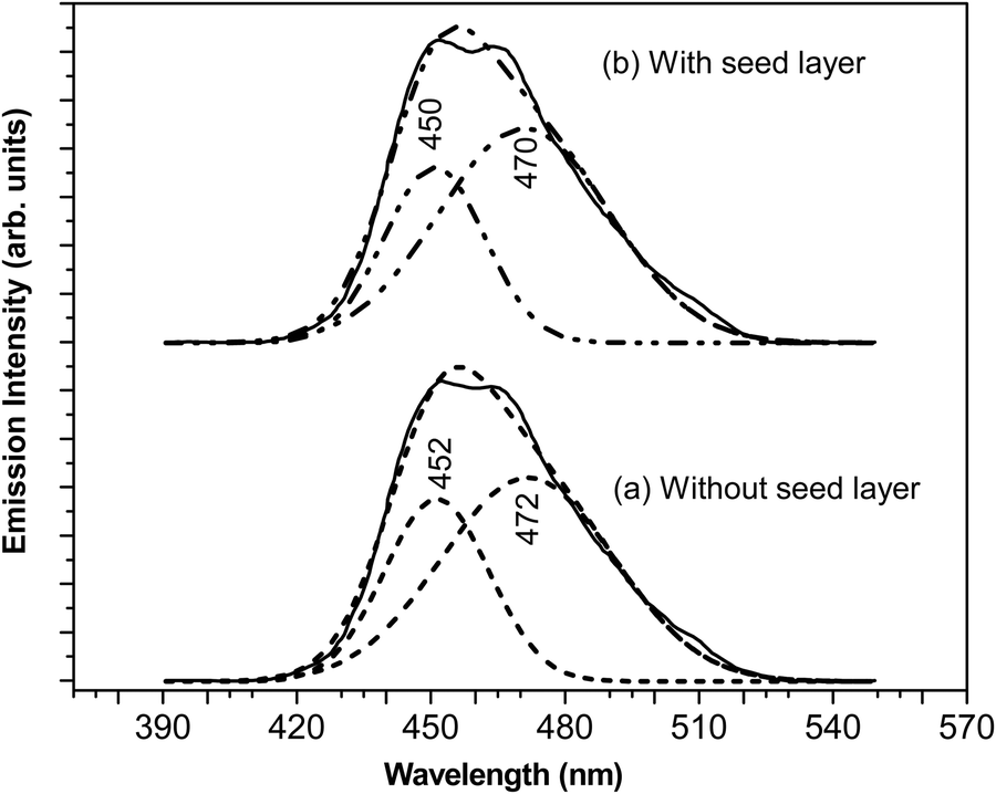 | ||
| Fig. 7 Fluorescence emission spectrum of ZnO colloidal dispersions in aqueous medium (a) without a seed layer and (b) with a seed layer. | ||
Moreover, the literature on size dependent fluorescence spectroscopy of ZnO nanoparticles shows that the fluorescence emission peak shifts from 360 nm to longer wavelengths.39,40 Multiple peaks in the range of 360 nm to 600 nm were observed for larger size nanoparticles as the size of the ZnO nanoparticles increases from 4.5 nm to 18 nm. Besides, the convoluted peak extends to 650 nm and thus, is very broad. The broadness of this peak besides the presence of peaks at higher wavelengths from 530 nm has been attributed to the presence of impurities besides oxygen related vacancies. Also, the additional peaks at 530 nm and higher wavelengths attributed to impurities were not observed, again as expected from our EDS and X-ray diffraction measurements. It may be kept in mind that the diameter of our nanorods has a distribution from 20 nm to 100 nm. Thus, the quality of synthesized ZnO nanorods is reasonably good, thus supporting the experimental observations from X-ray diffraction, Raman and EDS measurements.
As mentioned in the Experimental section, the as-synthesized ZnO nanorods were investigated for their utility as an active UV detection material. Fig. 8 shows the plot of measured photocurrent as a function of time upon exposure of the ZnO nanorod film to an Omnicure S 1000 UV-light source (320–500 nm). It is observed from the measured plots (inset of Fig. 8) that there is a rapid increase in photocurrent with an increase in the intensities of the incident light (ON state). Though five cycles (ON and OFF states) are shown for each of the source's intensity values in the graph, we did not notice any degradation in the sample.
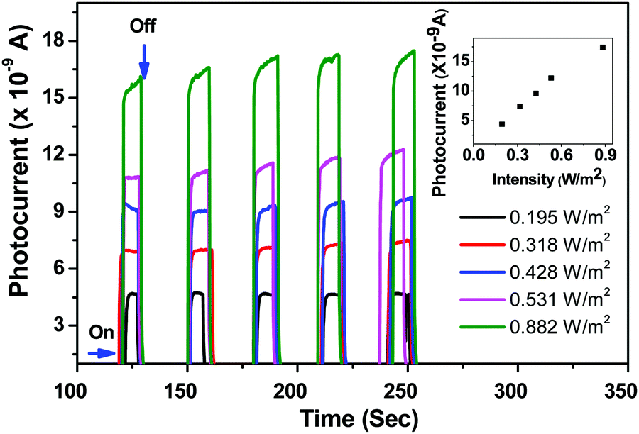 | ||
| Fig. 8 A plot of photocurrent generated as a function of time upon exposure of the ZnO nanorod film to an Omnicure S 1000 UV-light source (320–500 nm). The ON and the OFF states in the plot show the potential application in UV detection. The inset in the figure shows the peak photocurrent as a function of incident intensity. | ||
The UV detection mechanism of ZnO nanorods is defined on the basis of chemisorption and desorption of O2 and H2O molecules on the surface of the ZnO sample under UV irradiation. At room temperature O2 and H2O molecules from the atmosphere are chemisorbed and this process captures the electrons from the conduction band of ZnO samples. The loss of electrons from the conduction band due to the above process will enhance the depletion width in ZnO.
When the ZnO sample is exposed to UV light with different intensities photoelectrons are generated and neutralize the holes which result from chemisorption and this process decreases the depletion barrier height. As an alternative explanation we say that exposure to UV radiation results in photogenerated electrons some of which compensate the holes and others reach the conduction band to increase the photocurrent.
4. Conclusions
This work demonstrates the applicability of a template-free solvothermal method (a mixed solvent system of ethanol and water mixtures) to produce ZnO nanorods in powder and thin film forms at temperatures as low as 90 °C. The as-synthesized ZnO nanorods exhibit uniform structural and morphological properties. The X-ray diffractograms confirm that the ZnO nanorods exhibit a high degree of crystallinity and crystallize in a hexagonal lattice. The TEM and the SEM imaging reveals the size and the shape of the nanostructures grown in the solution phase and on the substrate as well. The nanorod morphology was pretty uniform throughout the sample as seen from SEM imaging recorded at low and high magnifications. While the average diameter of these nanorods was in the range of 20 to 100 nm, their lengths ranged from 700 nm to 1500 nm. The chemical composition was not only nearly stoichiometric (Zn at 51.54 atom% and oxygen at 48.46 atom%) but also, spatially homogeneous as confirmed from EDS measurements. Observation of an intense peak at 438 cm−1 in the Raman spectrum of the sample is attributed to the E2 (high) Raman-active phonon mode. More importantly, the E2 peak is nearly symmetric as seen from perfect Gaussian fits, implying the good crystalline quality of the synthesized nanorods. UV-Vis and fluorescence measurements were also carried out on colloidal aqueous dispersions of ZnO nanorods to determine their optical absorption and emission characteristics. An excitonic peak was observed at 370 nm for the colloidal dispersions of ZnO nanorods synthesized with 16 hours under refluxing conditions at 90 °C. The absorption coefficient in the range of 104–105 cm−1 in the visible region of the spectrum was determined, illustrating the semiconducting nature as expected. Values in the range of 3.3–3.4 eV for the band gap (Eg) of different types of ZnO nanorods prepared in this work were determined from Tauc plots, and these values lie very close to that measured for the single crystal ZnO bulk value. The measured fluorescence spectra of ZnO nanorods prepared in this work with and without a seed layer are nearly the same, in agreement with the crystallite size and similar amount of microstrain and dislocation density. Resolution of the characteristic (asymmetric) emission peak at 457 nm for neat ZnO nanorods observed in the fluorescence spectrum yields two peaks at 452 nm and 472 nm, which are attributed to zinc-related defect levels. However, we did not observe additional peaks at longer wavelengths, implying the absence of impurities, consistent with the analysis of data from other measurements discussed in this paper. Furthermore, the as-deposited ZnO nanorod film demonstrated its utility and potential as an active material to detect UV light. In short, the results confirm that the synthesized ZnO nanorods are of very good quality in terms of crystal structure, purity, uniformity in morphology, and stoichiometry in composition and that these nanorods can be produced in the large scale with good fluorescence emission in the visible range, auguring well for applications.Conflicts of interest
The authors affirm that they have no known competing financial interests or personal relationships that could appear to influence the work reported in this paper.References
- M. A. Chandran, N. Amal, K. M. Sreedhar, G. Sivasubramanian and K. M. Sreekanth, Rasayan J. Chem., 2020, 13, 2616–2625 CrossRef CAS.
- P. Gautham, U. Sachin Varma, K. M. Sreekanth, D. V. Ravi Kumar, K. M. Sreedhar and G. Sivasubramanian, Asian J. Chem., 2018, 30, 2631–2637 CrossRef CAS.
- Y. W. Heo, D. P. Norton, L. C. Tien, Y. Kwon, B. S. Kang, F. Ren, S. J. Pearton and J. R. Laroche, Mater. Sci. Eng., R, 2004, 47, 1–47 CrossRef.
- K. Y. Lee, M. K. Gupta and S. W. Kim, Nano Energy, 2015, 14, 139–160 CrossRef CAS.
- A. Mohandas, S. Deepthi, R. Biswas and R. Jayakumar, Bioact. Mater., 2018, 3, 267–277 CrossRef PubMed.
- N. M. Rohith, P. Kathirvel, S. Saravanakumar and L. Mohan, Optik, 2018, 172, 940–952 CrossRef.
- B. Weintraub, Z. Zhou, Y. Li and Y. Deng, Nanoscale, 2010, 2, 1573–1587 RSC.
- G. C. Yi, C. Wang and W. I. Park, Semicond. Sci. Technol., 2005, 20, S22–S34 CrossRef CAS.
- R. Thiruvengadathan, V. Korampally, A. Ghosh, N. Chanda, K. Gangopadhyay and S. Gangopadhyay, Rep. Prog. Phys., 2013, 76, 066501 CrossRef PubMed.
- X. M. Liu and Y. C. Zhou, J. Cryst. Growth, 2004, 270, 527–534 CrossRef CAS.
- S. Yamabi and H. Imai, J. Mater. Chem., 2002, 12, 3773–3778 RSC.
- J. Zhang, W. Wang, P. Zhu, J. Chen, Z. Zhang and Z. Wu, Mater. Lett., 2007, 61, 592–594 CrossRef CAS.
- C. H. Ahn, Y. Y. Kim, D. C. Kim, S. K. Mohanta and H. K. Cho, J. Appl. Phys., 2009, 105, 013502 CrossRef.
- W. Kim, M. Choi and K. Yong, Sens. Actuators, B, 2015, 209, 989–996 CrossRef CAS.
- K.-S. Kim and H. W. Kim, Phys. Rev. B: Condens. Matter Mater. Phys., 2003, 328, 368–371 CrossRef CAS.
- T. Okada, B. H. Agung and Y. Nakata, Appl. Phys. A: Mater. Sci. Process., 2004, 79, 1417–1419 CrossRef CAS.
- S. D. Shinde, G. E. Patil, D. D. Kajale, V. B. Gaikwad and G. H. Jain, J. Alloys Compd., 2012, 528, 109–114 CrossRef CAS.
- N. A. Abd Samad, C. W. Lai and S. B. Abd Hamid, Int. J. Photoenergy, 2016, 2016, 1413072 CrossRef.
- F. Aslan, A. Tumbul, A. Göktaş, R. Budakoğlu and İ. H. Mutlu, J. Sol-Gel Sci. Technol., 2016, 80, 389–395 CrossRef CAS.
- F. Mikailzade, H. Türkan, F. Önal, Ö. Karataş, S. Kazan, M. Zarbali, A. Göktaş and A. Tumbul, Appl. Phys. A: Mater. Sci. Process., 2020, 126, 768 CrossRef CAS.
- L. Suhaimi and A. H. Yuwono, IOP Conf. Ser.: Mater. Sci. Eng., 2019, 541, 012034 CAS.
- M. Khenfouch, M. Baïtoul and M. Maaza, Opt. Mater., 2012, 34, 1320–1326 CrossRef CAS.
- T. Dixit, I. A. Palani and V. Singh, RSC Adv., 2018, 8, 6820–6833 RSC.
- A. Janotti and C. G. Van De Walle, Phys. Rev. B: Condens. Matter Mater. Phys., 2007, 76, 165202 CrossRef.
- N. Khatun, S. Rani, G. Behera and S. Roy, J. Mater. NanoSci., 2022, 9, 74–78 CAS.
- B. D. Cullity, Elements of X-ray Diffraction, 1978 Search PubMed.
- R. Thiruvengadathan and O. Regev, Chem. Mater., 2005, 17, 3281–3287 CrossRef CAS.
- V. Mote, Y. Purushotham and B. Dole, J. Theor. Appl. Phys., 2012, 6, 6 CrossRef.
- P. Bindu and S. Thomas, J. Theor. Appl. Phys., 2014, 8, 123–134 CrossRef.
- A. Goktas, S. Modanlı, A. Tumbul and A. Kilic, J. Alloys Compd., 2022, 893, 162334 CrossRef CAS.
- M. S. Marques, V. F. Hernandes and J. R. Bordin, Phys. Chem. Chem. Phys., 2021, 23, 16213–16223 RSC.
- T. C. Damen, S. P.-S. Porto and B. Tell, Phys. Rev., 1966, 142, 570–574 CrossRef CAS.
- M. Yoshikawa, K. Inoue, T. Nakagawa, H. Ishida, N. Hasuike and H. Harima, Appl. Phys. Lett., 2008, 92, 113115 CrossRef.
- J. C. Manifacier, J. Gasiot and J. P. Fillard, J. Phys. E: Sci. Instrum., 1976, 9, 1002–1004 CrossRef CAS.
- V. Rakhesh, B. Shankar and V. K. Vaidyan, IOP Conf. Ser.: Mater. Sci. Eng., 2018, 012062 Search PubMed.
- R. N. Gayen, R. Bhar and A. K. Pal, Indian J. Pure Appl. Phys., 2010, 48, 385–393 CAS.
- J. Z. Marinho, F. C. Romeiro, S. C.-S. Lemos, F. V. Motta, C. S. Riccardi, M. S. Li, E. Longo and R. C. Lima, J. Nanomater., 2012, 2012, 427172 CrossRef.
- H. Zeng, G. Duan, Y. Li, S. Yang, X. Xu and W. Cai, Adv. Funct. Mater., 2010, 20, 561–572 CrossRef CAS.
- J. Estrada Urbina, A. Cruz-Alonso, M. Santander-González, A. Albores and A. Duran, Nanomaterials, 2018, 8, 247 CrossRef CAS PubMed.
- L. Irimpan, V. P.-N. Nampoori, P. Radhakrishnan, A. Deepthy and B. Krishnan, J. Appl. Phys., 2007, 102, 063524 CrossRef.
Footnote |
| † Dr Mengjun Bai could not be contacted to confirm the final author list prior to publication. All other authors agree with the addition of Ms Swati Dhua and Dr Sanju Rani as co-authors as they contributed to the work. |
| This journal is © The Royal Society of Chemistry 2022 |