
 Open Access Article
 This Open Access Article is licensed under a Creative Commons Attribution-Non Commercial 3.0 Unported Licence
Effect of joining temperature on the interconnection zone and electrical resistance of Ag/n-Mg2Si and Ag/n-Mg2Sn contacts†
Radhika
Deshpande
 *a,
Silvana
Tumminello
a,
Sahar
Ayachi
a,
Eckhard
Mueller
ab and
Johannes
de Boor
ac
*a,
Silvana
Tumminello
a,
Sahar
Ayachi
a,
Eckhard
Mueller
ab and
Johannes
de Boor
ac
aInstitute of Materials Research, German Aerospace Centre (DLR), Germany. E-mail: radhika.deshpande@dlr.de; johannes.deboor@dlr.de
bInstitute of Inorganic and Analytical Chemistry, Justus Liebig University of Giessen, Giessen, Germany
cInstitute of Technology for Nanostructures (NST), Faculty of Engineering, University of Duisburg-Essen, Germany
First published on 1st June 2022
Abstract
Mg2X (X = Si, Sn) based compounds are among the most viable materials for waste heat recovery due to their high thermoelectric figure of merit zT, abundance of the constituent elements, low mass density and environmental benignity. Naturally, to establish an improved life expectancy of thermoelectric devices, high zT must be complemented by robust joining between the thermoelectric legs and a metal electrode that causes only small thermal and electrical contact resistance. We have studied Ag as a potential electrode for n-Mg2Si and n-Mg2Sn TE materials and have systematically explored the influence of a variation of the joining temperature on the resulting interconnection zone (IZ) and the electrical contact resistance. With respect to the electrical contact resistance, a reasonably low value of < 20 μΩ cm2 for Mg2Si/Ag was found at 500 °C and a value of < 30 μΩ cm2 was obtained for Mg2Sn/Ag at 400 °C. At 450 °C, Mg2Si/Ag also showed a lower contact resistance (≈ 35 μΩ cm2) than Mg2Sn/Ag (≈165 μΩ cm2). Analyzing the observed phases, we can deduce that the superior interface quality of Mg2Si/Ag compared to Mg2Sn/Ag is not due to the electrical properties of the IZ itself. Instead the observed differences are presumably governed by microcracking which is less for Mg2Si/Ag, even though the coefficient of thermal expansion mismatch between Mg2Si and Ag is larger than that between Mg2Sn and Ag. We illustrate the use of phase diagrams to correlate IZ intermetallic layers to equilibrium phases to explain experimental observations of microstructures.
1. Introduction
Thermoelectricity contributes to a more sustainable usage of our Earth's resources by converting heat into electricity. It offers advantages over conventional fossil fuel-based conversion technologies for electricity supply in terms of environmental impacts and incurred cost. Thermoelectric generators (TEGs) are solid-state devices that have no moving parts and are free of any noise or vibrations. Additionally, these devices don’t produce any by-products, which makes this technology capable of delivering clean energy with high reliability at marginal maintenance costs. Due to these advantages, TEGs have been employed in deep space missions, remote data communication systems, climate control seat systems, polar weather stations, remote navigation systems and waste heat recovery applications in aerospace and automotive industries.1 In addition, TEGs have also been found to function by extracting human body heat for sourcing power in wearable electrocardiographic systems.2 For steady-demand applications, TEG efficiency becomes an important factor along with cost effectiveness.The performance of TEGs is governed by the figure of merit (ZT) of the device, which is given by3,4
 | (1) |
TEG efficiency is thus not only governed by the properties of the TE materials (n- and p-type joined functional legs) but also by the internal losses of the devices. Only if the device effects are small and the two materials are similar, the device ZT may be approximated by the figure-of-merit zT of the TE materials, which is given by
| zT = S2σT/κ | (2) |
An accepted technological target value for the ratio between Rc and R is lower than 10%.5 Therefore, for an optimal design of TEGs, the contact development is as important as the improvement of material performance.
Mg2Si and Mg2Sn-based TE materials are amongst the chosen materials due to their high TE properties,6–9 non-toxicity, low mass density and abundant availability of precursors. These properties make them suitable for commercial applications in automobiles, air and space industries. While solid solutions of Mg2Si and Mg2Sn exhibit superior TE properties8–11 they also suffer potentially from a limited thermodynamic stability due to a miscibility gap reported for the pseudo-binary phase diagram and Mg loss.12–15 On the other hand, n-Mg2Si has shown decent TE properties with zTmax > 0.716,17 and a higher stability against oxidation18 compared to Mg2Sn. Recent results have shown that p-Mg2Sn shows better properties than p-Mg2Si owing to a higher carrier mobility that results in a relatively high power factor.19 Likewise recently, n-Mg2Sn has been reported for a significant increase of zTmax to 1.2 through a proposed mechanism of self-compensation doping by largely growing interest in the material.20 Therefore, studies exploring Mg2Si and Mg2Sn are relevant in point of view of making a full Mg2X-based module.
A previous study of the binary Mg2Si and its contact development was conducted by de Boor et al.21,22 The study found out that Ni is a promising electrode which showed good adhesion and low electrical contact resistance with rc ∼ 4.4 ± 2.7 μΩ cm2. Cu was also tested as a potential candidate for both undoped23 and doped Mg2Si.24 The undoped Mg2Si resulted in a much higher rc ∼ 13.7 mΩ cm2![[thin space (1/6-em)]](https://www.rsc.org/images/entities/char_2009.gif) 23 than for the doped Mg2Si which had an rc around 44.3 μΩ cm2.24 Such a large difference in magnitude of rc between both cases have been attributed to the fact that rc may be charge carrier concentration dependent. Furthermore, Ag was tested as a joining electrode on both n- and p-type Mg2(Si,Sn)-based solid solutions due to its similar thermal expansion coefficient (CTE).25 SEM results showed no delamination of the Ag electrode and the growth of an interconnection zone (IZ) with newly formed, distinct phases between Mg2(Si,Sn) and Ag. Additionally, the differences in the microstructure of the IZs and the values of electrical contact resistances at 450 °C and 600 °C for both n- and p-type Mg2(Si,Sn) were reported. It was seen that a higher joining temperature decreases rc in n-type Mg2(Si,Sn). Based on this, the study inferred the formation of an in-situ diffusion barrier layer preventing further Ag diffusion into the TE material. Moreover, rc was found to be one order of magnitude higher in n-type Mg2(Si,Sn) than in p-type. Therefore, understanding the temperature-dependent phase evolution at the IZ may help us to reveal its relation with rc. Besides, the Mg2(Si,Sn) system has proven to demix not only after synthesis,13,26 but also after joining, notably after Cu and Ag joining.25,27–29 Therefore, conducting contact development studies on the binaries Mg2Si and Mg2Sn serves the purpose of less complex conditions. In this way, any influence of demixing of the matrix can be eliminated. Although after joining the microstructures of the Ag/n-Mg2(Si,Sn) and Ag/p-Mg2(Si,Sn) look similar, p-type samples show no change in carrier concentration close to the interface, while n-type samples show a noticeable depletion in charge carrier concentration. As n-type is superior to p-type with respect to the thermoelectric properties and a correlation of the IZ microstructure and the interface properties is of particular technological relevance, the n-type binaries Mg2Si and Mg2Sn were investigated in combination with an Ag electrode.
23 than for the doped Mg2Si which had an rc around 44.3 μΩ cm2.24 Such a large difference in magnitude of rc between both cases have been attributed to the fact that rc may be charge carrier concentration dependent. Furthermore, Ag was tested as a joining electrode on both n- and p-type Mg2(Si,Sn)-based solid solutions due to its similar thermal expansion coefficient (CTE).25 SEM results showed no delamination of the Ag electrode and the growth of an interconnection zone (IZ) with newly formed, distinct phases between Mg2(Si,Sn) and Ag. Additionally, the differences in the microstructure of the IZs and the values of electrical contact resistances at 450 °C and 600 °C for both n- and p-type Mg2(Si,Sn) were reported. It was seen that a higher joining temperature decreases rc in n-type Mg2(Si,Sn). Based on this, the study inferred the formation of an in-situ diffusion barrier layer preventing further Ag diffusion into the TE material. Moreover, rc was found to be one order of magnitude higher in n-type Mg2(Si,Sn) than in p-type. Therefore, understanding the temperature-dependent phase evolution at the IZ may help us to reveal its relation with rc. Besides, the Mg2(Si,Sn) system has proven to demix not only after synthesis,13,26 but also after joining, notably after Cu and Ag joining.25,27–29 Therefore, conducting contact development studies on the binaries Mg2Si and Mg2Sn serves the purpose of less complex conditions. In this way, any influence of demixing of the matrix can be eliminated. Although after joining the microstructures of the Ag/n-Mg2(Si,Sn) and Ag/p-Mg2(Si,Sn) look similar, p-type samples show no change in carrier concentration close to the interface, while n-type samples show a noticeable depletion in charge carrier concentration. As n-type is superior to p-type with respect to the thermoelectric properties and a correlation of the IZ microstructure and the interface properties is of particular technological relevance, the n-type binaries Mg2Si and Mg2Sn were investigated in combination with an Ag electrode.
Here, n-type Mg2Si/Ag and n-type Mg2Sn/Ag contacts are examined under various joining temperatures. n-type Mg2Si was joined with Ag at 450 °C, 500 °C, 550 °C, while n-type Mg2Sn was joined with Ag at 400 °C, 450 °C, 500 °C. These are the same samples as presented in our previous work30 but here, the contact properties are analysed by combining microstructural analysis and electrical contact resistance measurements. Phase diagrams were used to predict the composition of IZ intermetallic layers formed in equilibrium to look for correlation with the experimental observations.
2. Materials and methods
n-Type Mg2Si and Mg2Sn samples joined with Ag electrodes were fabricated by a two-step joining method. In this method, powder sintering and joining of the TE material with the electrode are done in two separate process steps. Polycrystalline Bi-doped Mg2Si and Mg2Sn powder of nominal compositions Mg2.06Si0.97Bi0.03 and Mg2.15Sn0.97Bi0.03 were fabricated by high energy ball milling of the elements. Stoichiometric amounts of elemental Mg [Mg turnings (Merck)], Si (<6 mm, ChemPur), Bi granule (99.999%, Goodfellow, ∼7 mm) and Sn (<71 μm, Merck), were weighed and transferred into stainless steel vials under inert atmosphere. Mg was taken with 3 at% excess19 for the synthesis of Mg2.06Si0.97Bi0.03 and 7.5 at% excess31 for the synthesis of Mg2.15Sn0.97Bi0.03, as previous research reported such nominal composition to give nearly phase pure materials. Excess Mg was taken in order to compensate for possible Mg losses caused by the high vapour pressure and reactivity of Mg.In order to obtain homogenous powder of Mg2.06Si0.97Bi0.03, milling was performed for around 12 h with intermittent hammering to chip off the materials stuck on the walls of the vials. For Mg2.15Sn0.97Bi0.03, the milling duration was around 4 h. A constant ball to powder ratio of 1.6 was employed during the whole milling procedure. Handling of the powder was done in a glove box under Ar atmosphere to avoid oxidation. After obtaining a homogenous powder, Mg2.06Si0.97Bi0.03 and Mg2.15Sn0.97Bi0.03 were subjected to sintering in a 15 mm diameter graphite die, under a pressure of 66 MPa. Mg2.06Si0.97Bi0.03 powder was sintered at 800 °C for 10 min and Mg2.15Sn0.97Bi0.03 powder was sintered at 600 °C, also for 10 min. The sintering was done utilizing a direct current sintering press (DSP, Dr Fritsch GmbH) with a heating rate of 1 K/s. The pressing conditions were chosen based on previous research to attain optimum TE properties.13,19,31
The density measurements for all the as-sintered pellets were done by Archimedes’ method, giving a relative density of >95% for all samples. X-Ray diffraction was performed on consolidated pellets to ensure phase-purity of the as-sintered materials utilizing a Siemens D5000 Bragg-Brentano diffractometer. The features used for the measurement were Cu-Kα radiation (1.5406 Å) in the 2θ range from 20° to 80° with a step size of 0.01°.
Local mappings of the Seebeck coefficient across the pellets were obtained by an in-house built Potential & Seebeck Scanning Microprobe (PSM)32 to ensure homogeneity of as-sintered samples in terms of TE properties and to determine the electrical contact resistances.
Joining with Ag electrodes was done in the same DSP facility by stacking four Ag foils (50 μm thickness each, VWR International GmbH) on each side of the pellet. The number of the stacked foils was chosen as such to allow for contact resistance measurements which have a limited lateral resolution. The process temperatures of the joining step were T = 450 °C, 500 °C, 550 °C for n-Mg2Si and T = 400 °C, 450 °C, 500 °C for n-Mg2Sn. All joining experiments were done under a holding time of 10 min and a pressure of 29 MPa.23,27 The joined samples were ground and cut to allow for SEM and PSM characterization. Both measurements were done along their cross-section after being cut, grinded and polished using an ethanol-based diamond solution. All measurements were performed on freshly ground surfaces to minimize possible oxidation. Seebeck profile scans and electrical contact resistance measurements were done using the PSM facility with a given uncertainty of <5%.32
3. Results
XRD measurements and Seebeck profile scanning were performed on the sintered pellets to confirm the composition and the homogeneity of the samples before joining with the Ag electrodes. PSM surface characterization of consolidated pellets of Mg2.06Si0.97Bi0.03 and Mg2.15Sn0.97Bi0.03 exhibit nearly homogeneous values of the surface Seebeck coefficient (figures provided in ESI,† S(1-2)). The Seebeck profile scanning of n-Mg2Si reveals a Seebeck value of approximately −55 μV K−1, while n-Mg2Sn exhibits a Seebeck value of approximately −80 μV K−1. Both values agree with the data previously reported in literature.16,33,34 XRD patterns of n-Mg2Si and n-Mg2Sn (figures provided in ESI,† S(3-4)) are identified according to the Inorganic Crystal Structure Database (ICSD).35 All the reflections from the main phase of Mg2Si and Mg2Sn are present, confirming the phase formation. The pattern measured on the Mg2Si sample is contemplated as XRD-wise phase pure as no additional reflexes belonging to any secondary phases were detected. As for the XRD pattern of Mg2Sn, all reflections from the main phase are present; however, additional small peaks corresponding to the secondary phases of Mg, SnO2, MgO and Bi2O6 were also detected. The Mg2Sn surface exhibited occasional cavities or pores, and as XRD measurements are done with a step size of 0.01°, these oxide phases may have formed during the measurement run or during the sintering step.SEM images of n-Mg2Si samples joined with Ag electrode are presented and discussed in the following section. Fig. 1(a–c) show the cross-section of n-Mg2Si samples joined with an Ag electrode at 450 °C, 500 °C and 550 °C, respectively. With Mg2Si, Ag shows good bonding with no delamination at all investigated temperatures. No cracks were observed along the joining interfaces; rarely, cracks inside the TE material are visible. Fig. 1(d–f) show SEM-BSE high magnification images of the interfaces of Mg2Si Joined with Ag at 450, 500, and 550 °C respectively.
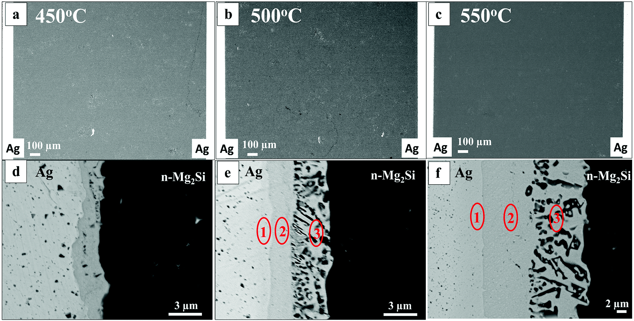 | ||
| Fig. 1 SEM-BSE images of n-Mg2Si joined with Ag at different temperatures – low magnification of the cross-section of n-Mg2Si joined with Ag (a) 450 °C, (b) 500 °C, (c) 550 °C; magnified view of n-Mg2Si/Ag interface joined at (d) 450 °C. (e) 500 °C, (f) 550 °C. | ||
The joining of the TE material with the electrode material resulted in a multi-layered IZ and an increasing layer thickness with increasing temperature. Fig. 1(d), corresponding to joining at 450 °C, displays a layer of ∼1–2 μm thickness, while the reaction layers resulting from joining at 500 °C and 550 °C (Fig. 1(e and f), respectively) are thicker (12–15 μm). A single reaction layer showing irregular mottled dark regions within the IZ is seen at 450 °C, while three distinct reaction layers (L 1, 2 and 3 as shown in Fig. 1(e and f)) are seen at 500 and 550 °C.
EDX elemental mapping of n-Mg2Si/Ag interfaces at 450 °C and 500 °C are presented in Fig. 2. The elemental distribution in the IZ at 550 °C was similar to that at 500 °C; therefore, it is not shown here. The element map of n-Mg2Si/Ag interface at 450 °C in Fig. 2(a) shows a single layer and the mottled dark regions containing mainly Si as highlighted by the white circle. For 500 °C in Fig. 2(b), a layer (L) sequence from left to right of Ag/L1/L2/Mg2Si can be seen where the Ag content gradually decreases across the layers towards Mg2Si. Mg content is high in L1 and in Mg2Si, while Si content is high only in layer L2 and in Mg2Si.
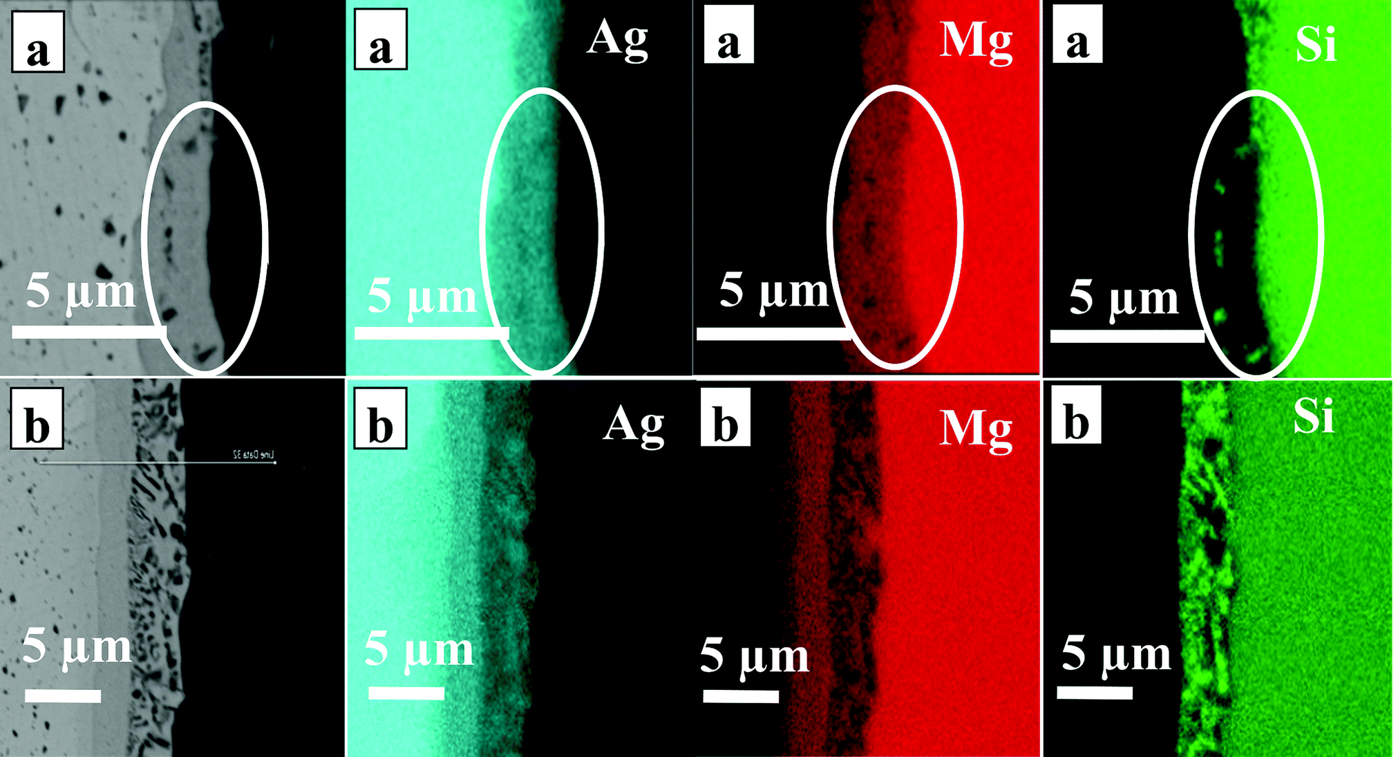 | ||
| Fig. 2 SEM-EDX element mappings of the IZs of n-Mg2Si/Ag formed at (a) 450 °C; (b) 500 °C. | ||
Fig. 3 shows cross sections of the Mg2.15Sn0.97Bi0.03/Ag interface regions of samples joined at 400 °C, 450 °C and 500 °C, respectively. Cracks were observed in the samples joined at 400 °C and 500 °C as shown in Fig. 3(a and c) respectively. At 500 °C, more cracks can be seen on both sides of the TE material, and the Ag electrode delaminated from one side of the sample (black area in Fig. 3(c)). No cracks were observed for the sample joined at 450 °C at the given magnification (Fig. 3(b)).
 | ||
| Fig. 3 SEM results of n-Mg2Sn joined with Ag at different temperatures – low magnification of the cross-section of n-Mg2Sn joined with Ag at (a) 400 °C; (b) 450 °C; (c) 500 °C; magnified view of n-Mg2Sn/Ag interface joined at (d) 400 °C; (e) 450 °C; (f) 500 °C (with the Ag foil being delaminated). | ||
At 400 °C and 450 °C one reaction layer is evident with a thickness of ∼10 μm, see Fig. 3(d and e). Such reaction layer, however, cannot be observed in Fig. 3(c and f) for the sample joined at 500 °C because of the cracks at the IZ. In fact, the Ag foil was only locally attached to the TE material at this joining temperature and part of the reaction layer is still visible on this sample, with a thickness of ∼6 μm as can be seen by the bright mottled regions on Fig. 3(f) and the remaining part of the reaction layer was attached on the Ag foil. This indicates that the cracking actually occurred inside a reaction layer, at a point where one of the newly-formed phases seems to have a weaker resistance to thermo-mechanical stress, most likely during cooling.
The EDX element maps of the interfaces of n-Mg2Sn/Ag at 400 °C and 500 °C are presented in Fig. 4(a and b) respectively. Both figures indicate the simultaneous presence of Mg, Ag and Sn in the reaction layer. Bi segregation was also seen as shown in Fig. 4(a). A line scan was also processed across the interface layer of the sample joined at 450 °C and is presented in Fig. 8(b). Both the element mapping and the line scan, along with composition point analysis at the interface processed at 450 °C reveal a phase containing all three elements, corresponding approximately to Mg32Ag60Sn8 with a slight gradient in the values as can be noticed from the line scan.
 | ||
| Fig. 4 SEM-EDX results of IZs n-Mg2Sn/Ag formed at (a) 400 °C; (b) 450 °C. | ||
4. Electrical contact resistance calculations
The electrical contact resistance (Rc) is calculated based on PSM measurements.32 In the case of an ideal sample, which means that the sample and the contacts are homogenous, the current, I, passing through the sample of cross-sectional area, A, is uniformly distributed across the sample and the contact areas. In such an ideal case, the current density is constant, given by j = I/A and the contact resistance Rc can be calculated by using eqn (3).| Rc = (Vel − VTE)/I | (3) |
However, the homogeneity of the current density cannot be guaranteed in real samples, as irregularities and inhomogeneities cannot be avoided most of the times. In such non-ideal cases, the current is not homogeneously distributed anymore, which results in a non-homogenous current density. In this case, the specific contact resistance is also calculated following eqn (4).
| rc = Rc·A = (Vel − VTE)/j | (4) |
| j = ΔVTE/(ρTElTE) | (5) |
Fig. 5 shows exemplary Seebeck and potential line scans of n-Mg2Si samples joined at 450 °C (a), 500 °C (b), 550 °C (c) and n-Mg2Sn samples joined at 400 °C (d), 450 °C (e) and 500 °C (f). As the Ag foil on the n-Mg2Sn sample joined at 500 °C was completely delaminated from both sides during sample cutting, only the Seebeck coefficient could be measured for that sample.
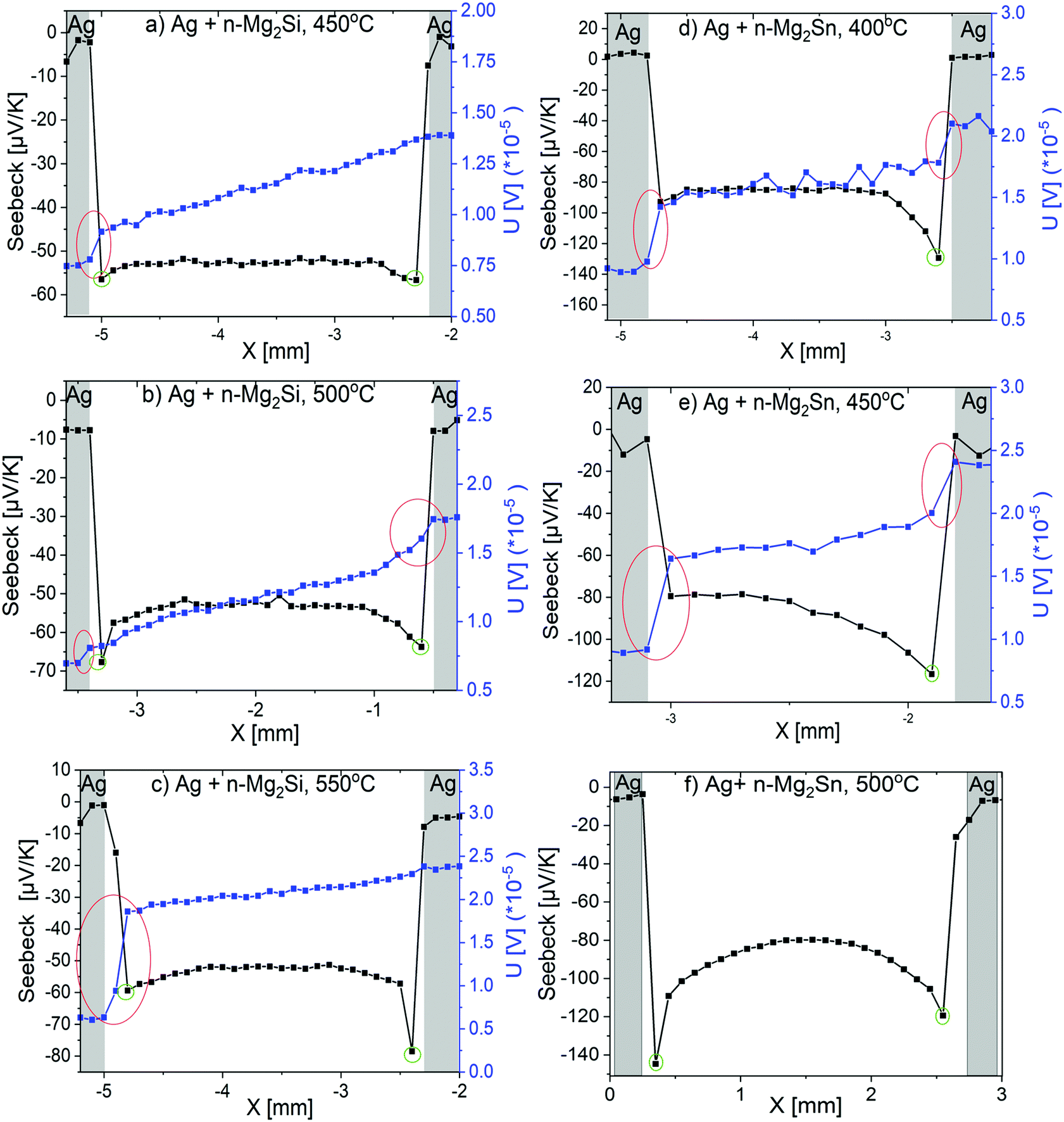 | ||
| Fig. 5 PSM line scans of (a) Ag + n-Mg2Si joined at 450 °C; (b) Ag + n-Mg2Si at 500 °C; (c) Ag + n-Mg2Si at 550 °C; (d) Ag + n-Mg2Sn at 400 °C; (e) Ag + n-Mg2Sn at 450 °C; (f) Ag + n-Mg2Sn at 500 °C. The red circles in the figures indicate the potential drop, the green circles indicate the lowest Seebeck coefficient value close to the interface. Modified image from our previous work.30 | ||
From Fig. 5, it is generally observed that the potential lines across the TE material are more linear when there are less cracks in the sample, which is the case for the Mg2Si samples, compared to the Mg2Sn samples. A potential drop is observed near the interfaces as shown by the red circles in Fig. 5(a–e). These drops are seen only on one side in the n-Mg2Si samples (Fig. 5(a–c)), but are seen on both sides in n-Mg2Sn (Fig. 5(d and e)). Such behaviour may be associated with the presence of micro-cracks near the interface or within the evolved phases. The potential graph is noisy for the Mg2Sn sample joined at 400 °C (Fig. 5(d)) indicating a low current density. This might arise e.g. from large interface resistances between sample and the measurement device.
The calculated rc values are given in Table 1. The average of all valid PSM graphs are taken into account for the computation of the final rc values by using eqn (3) (PSM values) and eqn (4). The current densities are calculated by eqn (5) by considering the intrinsic TE properties after joining and the PSM current densities are given by IPSM/A.28 As the rc values are different for both sides, they are separately indicated in the table as left and right side of the figure. The reliability of the results of this table can be validated by comparing the values from eqn (3) and (4). The results of eqn (4) are likely less affected by sample inhomogeneities. Also, the measured contact resistance contains a contribution from the TE material itself, due to the limited spatial resolution. Rough estimates show that this contribution is smaller than a few percent of the total contact resistance and can therefore be neglected.
| Contact | Joining temperature (°C) | j (A cm−2) | r c (μΩ cm2) | ||||
|---|---|---|---|---|---|---|---|
| Eqn (5) | I PSM/A | Eqn (4) | Eqn (3) | ||||
| Left | Right | Left | Right | ||||
| Mg2.06Si0.97Bi0.03/Ag | 450 | 0.038 | 0.029 | 35 ± 12 | 7 ± 6 | 48 ± 17 | 9 ± 8 |
| 500 | 0.063 | 0.022 | 9 ± 4 | 17 ± 8 | 24 ± 13 | 52 ± 24 | |
| 550 | 0.029 | 0.022 | 389 ± 71 | 32 ± 9 | 511 ± 94 | 42 ± 13 | |
| Mg2.15Sn0.97Bi0.03/Ag | 400 | 0.042 | 0.052 | 8 ± 5 | 26 ± 14 | 2 ± 1 | 7 ± 4 |
| 450 | 0.016 | 0.035 | 137 ± 56 | 60 ± 36 | 175 ± 71 | 76 ± 46 | |
Previous research on Ag electrode joining with n-Mg2(Si,Sn) reports a decrease in rc value as temperature increases from 450 °C to 600 °C.25 However, in this study as we can see from Table 1, for n-Mg2Si/Ag, rc doesn’t change monotonously from 450 to 550 °C. As we have seen a systematic increase of the IZ thickness with joining temperature this speaks against a strong correlation between contact resistance and IZ layer thickness. For the n-Mg2Sn samples, lowering the joining temperature from 450 °C to 400 °C lowered the rc value. If we take a look at the current density values from Table 1 calculated by eqn (5) and from PSM assuming a constant j throughout the samples, we observe a difference of a factor of 2 to 3, showing that the local current density is not that as expected from the bulk conductivities. This discrepancy can come from inhomogeneities caused by the cracks inside/near the IZ which affect the local current distribution. This also affects the calculation of the contact resistance, but more for the result by eqn (3) than that by eqn (4).
Also, note the increase in the absolute Seebeck coefficient values near the IZ which is shown by the green circles in Fig. 5(a–f). This behaviour was related to the depletion of charge carriers near the interface as Ag acts as a p-type dopant for n-type materials.30 The thickness of the depleted layer can be read from the Seebeck coefficient as the range the Seebeck coefficient is different from the bulk value of ∼−55 μV K−1 of n-Mg2Si before joining. The diffusion length of Ag as determined from PSM line scans cannot be determined from EDX line scans since the amount of Ag is below the detection limit of the EDX detector. The depleted layer thickness systematically increases from ∼0.25 mm at 450 °C to ∼0.5 mm at 500 °C and further to ∼0.6 mm at 550 °C for n-Mg2Si samples. For the n-Mg2Sn samples Fig. 5(d and e), the thickness of depleted layer is larger for the sample joined at 450 °C than the sample joined at 400 °C. The Seebeck value drops to ∼−120 μV K−1 for both temperature points and goes back to the normal Seebeck value (∼−83 μV K−1) after around ∼0.35–0.45 mm and ∼0.4–0.7 mm respectively for the samples joined at 400 and 450 °C. Moreover, as is displayed by the Seebeck profile lines, the diffusion of Ag in n-Mg2Sn is less homogeneous than in n-Mg2Si. In fact, the diffusion lengths of Ag are not comparable on both sides in the n-Mg2Sn samples, unlike it is observed for Mg2Si.
5. Discussion
5.1 Phase equilibria considerations regarding the interconnection zone
To investigate the complex phenomena taking place in the IZ and to correlate the microstructural observations we consider equilibrium diagrams. We investigate elemental affinity and phase transformations in n-Mg2Si/Ag and n-Mg2Sn/Ag contacts from the equilibrium thermodynamics point of view. We combine chemical analysis by EDX with calculated isothermal sections of the Ag–Mg–Si and Ag–Mg–Sn systems to qualitatively correlate the observed layers with the equilibrium phases at the IZ with respect to a systematic increase of temperature. The fundamentals of atomic transport and phase transformations let us state that the growth of the intermetallic layers is characterized by a limiting mechanism which is either mass diffusion or interface reaction controlled (nucleation and growth) or mixed. The initial stage of the formation of the reaction layers is characterized by diffusion of the elements towards or through the interface. The difference in atomic chemical potentials at the IZ will result in a flux of mass towards the initial interface and subsequent reactions (phase transformations). These reactions form new phases that grow at the original interface, which in turn creates new interfaces and modifies the diffusion–reaction layer growth process. Although a quantitative investigation of growth mechanisms falls outside the scope of the present work, it is possible to qualitatively formulate conclusion on the initial phenomena at the IZ.The three constitutive binaries of the Ag–Mg–Si system, e.g. Ag–Mg, Mg–Si and Si–Ag are presented in Fig. 6(a–c) with the investigated joining temperatures indicated; the calculations were done with the Thermo-Calc software and the thermodynamic database TCMG5.36 From the Ag–Si phase diagram, it is worth mentioning the low affinity between Ag–Si which form no intermediate phases, in contrast to the Ag–Mg system where Mg shows high affinity for Ag and therefore reaction at the interfaces is expected. In particular, note the high solubility of Mg in Ag forming (Ag) terminal FCC-type solid solution and the wide composition range of the intermediate phase BCC-AgMg.
 | ||
| Fig. 6 Calculated phase diagrams of the binary systems (a) Ag–Mg; (b) Mg–Si; (c) Si–Ag; (d) Ag–Mg; (e) Mg–Sn; (f) Sn–Ag. The purple, green, red and cyan dashed lines, respectively, indicate the temperatures 400, 450, 500 and 550 °C. | ||
A ternary isothermal section for the Ag–Mg–Si system at 500 °C was calculated using the same thermodynamic database and is presented together with the line scan chemical analysis in Fig. 7. The Ag–Mg–Si shows no ternary phase according to the thermodynamic description in TCMG5. The black dashed line is an eye-guide to portray the two parts to be joined, namely, Mg2Si and Ag, however it does not represent the real composition evolution of the bonded region during the joining time. After 10 min at 500 °C the bonded region of Mg2Si/Ag showed the configuration Mg2Si/L3/L2/L1/Ag as in Fig. 7(a). Layer compositions are indicated by the line scan and the point analysis presented in Table 2. A SEM/EDX point analysis of n-Mg2Si/Ag related to the Table 2 is presented in ESI,† in S5.
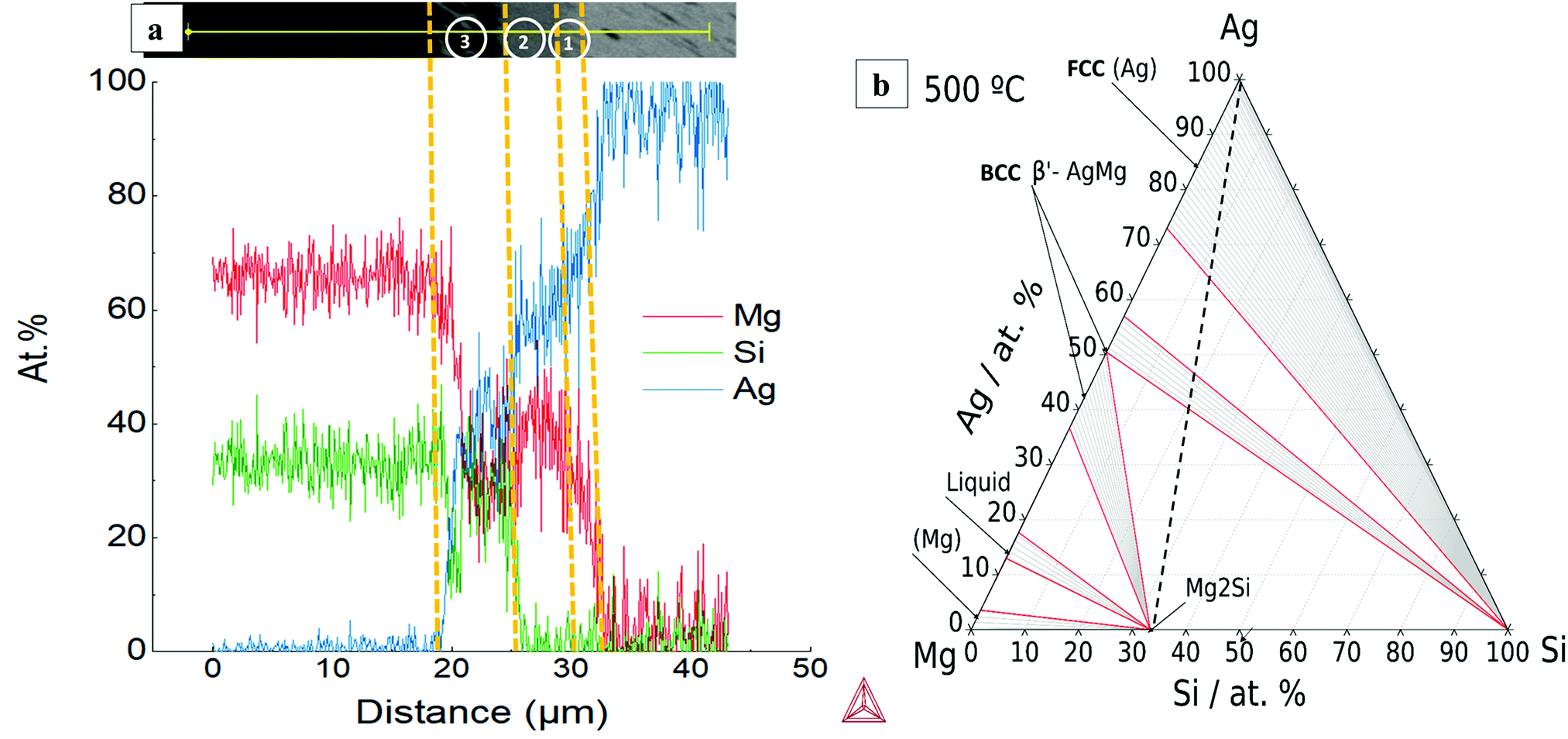 | ||
| Fig. 7 (a) EDX line scan of n-Mg2Si/Ag at 500 °C where 1, 2 and 3 are reaction layers; (b) isotherm of Ag–Mg–Si system at 500 °C. | ||
| Composition (at%) | |||
|---|---|---|---|
| Layer 1 | Layer 2 | Layer 3 | |
| Mg | ∼24 | ∼36 | ∼28 |
| Ag | ∼75 | ∼64 | ∼44 |
| Si | ∼1 | ∼1.3 | ∼27 |
| Plausible phase | Fcc (Ag) | AgMg | AgMg + Si islands |
By comparing with the equilibrium diagram, L1 can be associated with (Ag) terminal solution dissolving 24 at% Mg in equilibrium with very small amounts of elemental Si (less than 1 at% Si) as shown in the phase diagram by the equilibrium lines in the (Ag) + Si field. The next layer, L2, is then the AgMg phase in the Ag-rich region in equilibrium with slightly more Si than L1, ∼1.3 at% Si. The elemental profile shown by the line scan is in agreement with the composition range of stability of the AgMg phase (∼36–58 at%Ag). The agreement between our measurements and the calculated phase boundaries of AgMg is good enough considering that the processing methods deviate from equilibrium conditions and that a thermodynamic assessment of this ternary is desired. Finally, L3 consists of two phases as can be better seen in Fig. 1 and the elemental mapping in Fig. 2. Such a multiphase layer is possible in the case of ternaries and higher order systems. L3 can be associated with AgMg phase + Si, falling in the three-phase region of the phase diagram, Mg2Si + AgMg + Si. The layers/phases association results for Mg2Si/Ag at 550 °C are similar to 500 °C differing only in the composition ranges. Whereas for 450 °C the single layer observed is related to the (Ag) terminal solution in equilibrium with even less amounts of Si with respect to the same layer at higher temperatures. Similar observations were previously reported while discussing the Mg2(Si,Sn)/Ag IZ at 450 and 600 °C.25
For the n-type Mg2Sn/Ag contacts, we calculated the constitutive binaries of the Ag–Mg–Sn system as shown in Fig. 6(d–f) indicating the joining temperatures. We can observe that at all the joining temperatures the liquid phase can be present due to the low melting temperature of the Sn. From the binary phase diagrams, we can deduce the higher affinity between the elements, Sn and Ag, in contrast to the previous case, Si and Ag. As anticipated from the binaries, the calculated isotherm at 450 °C shows significant ternary extensions of the binary phases, see Fig. 8b. The IZ of n-Mg2Sn/Ag after 10 min at 450 °C evidences one single layer, Mg2Sn/L1/Ag, with wavy interfaces and isolated regions next to Mg2Sn, see Fig. 8a. Such a roundish morphology indicates the presence of a liquid phase at 450 °C. By comparing the line scan compositions with the phase diagram, we can see that the single intermediate layer, L1, has a composition of Ag between ∼50–65 at% Ag, which agrees with the composition range of AgMg phase in the Ag-rich side. AgMg dissolves ∼10 at% Sn as seen from the line scan. The phase diagram shows that the AgMg phase extends dissolving Sn also up to ∼10 at% Sn. Furthermore, the isothermal section shows that AgMg is in equilibrium with the liquid phase as seen in the AgMg + liquid field. A SEM/EDX spot analysis of n-Mg2Sn/Ag joined at 450 °C is presented in ESI,† in S6.
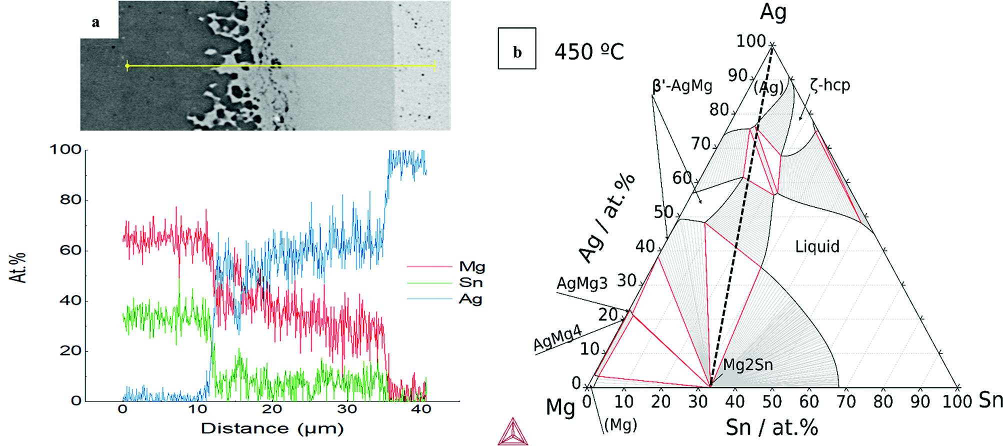 | ||
| Fig. 8 (a) EDX line scan of n-Mg2Sn/Ag at 450 °C (b) Isotherm of the Ag–Mg–Sn system at 450 °C. | ||
The thermodynamic analysis can also help to understand the observed changes in the Seebeck coefficient close to the IZ better. While it was explained in25,30 that Ag diffusion is the origin, the information deducible from the microstructure of the IZ has been ignored. One might wonder if the formed phases hinder diffusion of Ag. For both n-Mg2Si/Ag and n-Mg2Sn/Ag the IZ consists of (Ag) and/or AgMg as main phases, which both have a relatively simple crystallography: (Ag) is FCC-A1 and AgMg is BCC-B2.37 FCC-A1 demonstrates equal probability for all atoms to occupy at all equivalent sites in the crystal structure and BCC-B2 provides two equivalent sites with a different probability for the atoms, one at the centre and the other at the corners. Neither (Ag) nor AgMg can therefore be expected to prevent the diffusion of Ag atoms into the TE material.
5.2 Analysing the influence of the presence of intermetallic layers at the interconnection zone on the final contact resistance
One might further argue that, as the joining temperature influences the resulting layer/phase sequence and layer thickness in the IZ, it may also have an effect on the final electrical contact resistance. In n-Mg2Si/Ag, the IZ is spread over a broader Ag composition range. We have (Ag) next to Mg2Si for 450 °C and (Ag) and AgMg for the higher T. To have an approximate idea, we calculated, using Thermo-Calc software and TCAL/Al-alloys database version 7,38 the electrical resistivity of (Ag) (ρ < 2 × 10⁻⁷ Ω m for xMg < 0.25) and AgMg (ρ < 1.53 × 10⁻⁶ Ω m for xMg < 0.65) phases at 500 °C which is approximately two orders of magnitude lower than that of the TE materials (resistivity 10−5–10−4 Ω m). As the thickness of these conductive intermetallic layers that form the IZ are only a few μm they don’t constitute a significant fraction of the measured contact resistance. At 500 and 550 °C, precipitation of Si islands has been observed (see Fig. 2 and ESI†). It is likely that these Si islands are responsible to make the IZ less conductive than at 450 °C. However, as these form isolated islands and make up only some vol% the effect can be expected to be insignificant as well. Furthermore, we observe that rc on both sides of this sample differs by a factor of 10 at 550 °C while the microstructure is similar. For n-Mg2Sn/Ag also MgAg was formed at the IZ (but with a different composition) but moderately high electrical contact resistances were measured.6. Conclusions
In this work, we investigated the morphology, composition and contact resistance of interconnection zones (IZ) between both n-type Mg2Si and n-type Mg2Sn, and Ag as an electrode material. The contacts were fabricated using a two-step process where the joining experiments are done using pre-sintered pellets of the TE material. We observed relatively low values of electrical contact resistance ≈17 μΩ cm2 for the n-Mg2Si/Ag at 500 °C and ≈35 μΩ cm2 for the n-Mg2Si/Ag at 450 °C. For n-Mg2Sn/Ag, a value of <30 μΩ cm2 was obtained at 400 °C. We also correlated the systematic experimental observations of the evolution of distinct intermetallic layers in the IZ with the calculated phase diagrams to obtain layer-to-phase relations. It was shown that the thermodynamic study can be used to:• Predict the equilibrium composition of the intermetallic layers formed at IZ of n-Mg2Si/Ag and n-Mg2Sn/Ag,
• Gain an insight into the microstructure and the morphology in the reacted IZ leading to a possible growth sequence for the intermetallic layers,
• Understand that the formed IZ will not stop Ag diffusion, indicating the need of a diffusion barrier to prevent contamination of n-type Mg2(Si,Sn) by Ag,
• Confirm that the “bulk” properties of the IZ do not affect the observed electrical contact resistances significantly.
With respect to the observed contact resistances we can conclude that the electrical properties of the IZ is not the main origin. A dependence on carrier concentration is in principle plausible (e.g. ref. 23), however, we don’t observe a correlation between the Seebeck coefficient S (and hence carrier density n) and rc for our samples. Moreover, we note that even the increased absolute values of S correspond to carrier concentrations n ∼ 1020,30 the samples thus presumably remain highly doped at the interface. This leaves (micro-)cracks as the most plausible origin of the high contact resistances. In this regard it is interesting to note that Ag is CTE-wise closer to Mg2Sn than Mg2Si,25 yet the bonding worked better for n-Mg2Si/Ag than for n-Mg2Sn/Ag and less cracks were observed for the former. This shows that the CTE match is not the only criterion to assure good properties of the joining and a holistic approach is required for selection of an electrode for joining a TE material with.
Author contributions
Radhika Deshpande: Methodology, validation, formal analysis, investigation (experimental), writing – original draft, visualization. Silvana Tumminello: formal analysis, validation, writing – review & editing. Sahar Ayachi: validation, writing – review & editing, supervision. Eckhard Müller: writing – review & editing, supervision. Johannes de boor: conceptualization, methodology, writing – review & editing, supervision, project administration.Conflicts of interest
The authors declare no financial or commercial conflict of interest.Acknowledgements
The authors would like to gratefully acknowledge the endorsement for the DLR executive Board Members for Space Research and Technology, as well as the financial support from the Young Research Group Leader Program. J. D. B. is supported by the Deutsche Forschungsgemeinschaft (DFG, German Research Foundation), project number 396709363. We would also like to thank Pawel Ziolkowski and Przemyslaw Blaschkewitz from DLR for their help and assistance with the thermoelectric measurements.Notes and references
- L. E. Bell, Cooling, heating, generating power, and recovering waste heat with thermoelectric systems, Science, 2008, 321(5895), 1457–1461 CrossRef CAS PubMed.
- M. Dargusch, W.-D. Liu and Z.-G. Chen, Thermoelectric Generators: Alternative Power Supply for Wearable Electrocardiographic Systems, Adv. Sci., 2020, 7(18), 2001362 CrossRef CAS PubMed.
- D. K. Aswal, R. Basu and A. Singh, Key issues in development of thermoelectric power generators: High figure-of-merit materials and their highly conducting interfaces with metallic interconnects, Energy Conversion Manage., 2016, 114, 50–67 CrossRef.
- S. Priya and D. J. Inman, Energy harvesting technologies, Springer, 2009, vol. 21 Search PubMed.
- D. M. Rowe, Conversion efficiency and figure-of-merit, 1995, p. 31 Search PubMed.
- A. Sankhla, et al., Mechanical Alloying of Optimized Mg2(Si,Sn) Solid Solutions: Understanding Phase Evolution and Tuning Synthesis Parameters for Thermoelectric Applications, ACS Appl. Energy Mater., 2018, 1(2), 531–542 CrossRef CAS.
- W. Liu, X. Tang and J. Sharp, Low-temperature solid state reaction synthesis and thermoelectric properties of high-performance and low-cost Sb-doped Mg2Si0.6Sn0.4, J. Phys. D: Appl. Phys., 2010, 43(8), 085406 CrossRef.
- W. Liu, et al., Convergence of Conduction Bands as a Means of Enhancing Thermoelectric Performance of n-Type Mg2Si1−xSnx Solid Solutions, Phys. Rev. Lett., 2012, 108(16), 166601 CrossRef PubMed.
- V. K. Zaitsev, et al., Highly effective Mg2Si1−xSnx thermoelectrics, Phys. Rev. B: Condens. Matter Mater. Phys., 2006, 74(4), 045207 CrossRef.
- T. Dasgupta, et al., Influence of power factor enhancement on the thermoelectric figure of merit in Mg2Si0.4Sn0.6 based materials, Phys. Status Solidi A, 2014, 211(6), 1250–1254 CrossRef CAS.
- H. Kamila, et al., Analyzing transport properties of p-type Mg2Si–Mg2Sn solid solutions: optimization of thermoelectric performance and insight into the electronic band structure, J. Mater. Chem. A, 2019, 7(3), 1045–1054 RSC.
- M. Yasseri, et al., Influence of Mg loss on the phase stability in Mg2X (X = Si, Sn) and its correlation with coherency strain, Acta Mater., 2021, 208, 116737 CrossRef CAS.
- M. Yasseri, et al., Solid solution formation in Mg2(Si,Sn) and shape of the miscibility gap, Acta Mater., 2020, 185, 80–88 CrossRef CAS.
- I.-H. Jung, et al., Thermodynamic modeling of the Mg–Si–Sn system, Calphad, 2007, 31(2), 192–200 CrossRef CAS.
- R. Orenstein, et al., Using phase boundary mapping to resolve discrepancies in the Mg2Si–Mg2Sn miscibility gap, J. Mater. Chem. A, 2021, 9(11), 7208–7215 RSC.
- S. K. Bux, et al., Mechanochemical synthesis and thermoelectric properties of high quality magnesium silicide, J. Mater. Chem., 2011, 21(33), 12259–12266 RSC.
- J. de Boor, et al., Fabrication parameters for optimized thermoelectric Mg2Si, J. Mater. Sci., 2014, 49(8), 3196–3204 CrossRef CAS.
- E. M. Godlewska, et al., Reaction and diffusion phenomena in Ag-doped Mg2Si, J. Alloys Comds., 2016, 657, 755–764 CrossRef CAS.
- H. Kamila, et al., Synthesis of p-type Mg2Si1−xSnx with x = 0–1 and optimization of the synthesis parameters, Mater. Today: Proc., 2019, 8, 546–555 CAS.
- Y. Zhu, et al., Thermodynamic criterions of the thermoelectric performance enhancement in Mg2Sn through the self-compensation vacancy, Mater. Today Phys., 2021, 16, 100327 CrossRef CAS.
- J. de Boor, et al., Thermal Stability of Magnesium Silicide/Nickel Contacts, J. Electron. Mater., 2016, 45(10), 5313–5320 CrossRef CAS.
- J. de Boor, et al., Fabrication and characterization of nickel contacts for magnesium silicide based thermoelectric generators, J. Alloys Compd., 2015, 632, 348–353 CrossRef CAS.
- L. Cai, et al., Duration of Thermal Stability and Mechanical Properties of Mg2Si/Cu Thermoelectric Joints, J. Electron. Mater., 2018, 47 CAS.
- A. Ferrario, et al., Mechanical and Electrical Characterization of Low-resistivity Contact Materials for Mg2Si, Mater. Today: Proc., 2015, 2(2), 573–582 Search PubMed.
- N. H. Pham, et al., Ni and Ag electrodes for magnesium silicide based thermoelectric generators, Mater. Today Energy, 2019, 11, 97–105 CrossRef CAS.
- A. Kozlov, J. Gröbner and R. Schmid-Fetzer, Phase formation in Mg–Sn–Si and Mg–Sn–Si–Ca alloys, J. Alloys Compd., 2011, 509(7), 3326–3337 CrossRef CAS.
- S. Ayachi, et al., Developing Contacting Solutions for Mg2Si1−xSni-Based Thermoelectric Generators: Cu and Ni45Cu55 as Potential Contacting Electrodes, ACS Appl. Mater. Interfaces, 2019, 11(43), 40769–40780 CrossRef CAS PubMed.
- S. Ayachi, et al., Contacting Cu Electrodes to Mg2Si0.3Sn0.7: Direct vs. Indirect Resistive Heating, Semiconductors, 2019, 53(13), 1825–1830 CrossRef CAS.
- S. Jayalakshmi, et al., Effect of Ag and Cu trace additions on the microstructural evolution and mechanical properties of Mg–5Sn alloy, J. Alloys Compd., 2013, 565, 56–65 CrossRef CAS.
- S. Ayachi, et al., On the relevance of point defects for the selection of contacting electrodes: Ag as an example for Mg2(Si,Sn)-based thermoelectric generators, Mater. Today Phys., 2021, 16, 100309 CrossRef CAS.
- A. Sankhla, et al., Experimental investigation of the predicted band structure modification of Mg2X (X: Si, Sn) thermoelectric materials due to scandium addition, J. Appl. Phys., 2019, 125(22), 225103 CrossRef.
- D. Platzek, et al., Potential-Seebeck-microprobe (PSM): measuring the spatial resolution of the Seebeck coefficient and the electric potential, in ICT 2005, 24th International Conference on Thermoelectrics, 2005.
- J.-I. Tani, T. Shinagawa and M. Chigane, Thermoelectric Properties of Impurity-Doped Mg2Sn, J. Electron. Mater., 2019, 48(5), 3330–3335 CrossRef CAS.
- H. Y. Chen and N. Savvides, Microstructure and Thermoelectric Properties of n- and p-Type Doped Mg2Sn Compounds Prepared by the Modified Bridgman Method, J. Electron. Mater., 2009, 38(7), 1056–1060 CrossRef CAS.
- M. Hellenbrandt, The Inorganic Crystal Structure Database (ICSD)—Present and Future, Crystallogr. Rev., 2004, 10(1), 17–22 CrossRef CAS.
- TCMG5, Thermo-Calc Mg-based Alloys Database version 5, accessed: 27 August 2021.
- W. G. Henry and G. V. Raynor, Superlattice Studies In The Systems Silver–Magnesium–Tin And Silver–Magnesium–Zinc, Canadian J. Phys., 1952, 30(5), 412–421 CrossRef CAS.
- TCMG7, Thermo-Calc Software TCAL/Al-alloys database version 7, accessed: 26 October 2021.
Footnote |
| † Electronic supplementary information (ESI) available. See DOI: https://doi.org/10.1039/d2ma00038e |
| This journal is © The Royal Society of Chemistry 2022 |