DOI:
10.1039/D2MA00023G
(Paper)
Mater. Adv., 2022,
3, 3994-4005
Flexible, environmentally-acceptable and long-durable-energy-efficient novel WS2–polyacrylamide MOFs for high-performance photodetectors†
Received
9th January 2022
, Accepted 15th March 2022
First published on 6th April 2022
Abstract
In this work, two-dimensional WS2–polyacrylamide metal–organic frameworks (MOFs) are prepared via an energy-efficient solvent-free frontal polymerization method and further used as a biocompatible, flexible, and low threshold high-performance photodetection. For fabricating biocompatible and flexible photodetector devices, these MOFs are coated on a normal paper substrate and carbon nanotubes are used as the electrodes. Scanning and tunneling electron microscopy (SEM and TEM) images exhibit the nanosheet-like structure and clear incorporation of WS2 nanosheets in a polyacrylamide matrix. X-ray photoelectron spectroscopy (XPS) analysis shows the peaks of W 5p3/2, W 4f3/2, and W 4f7/2 at the binding energies of 38.48, 34.98, and 32.88 eV, confirming the presence of W with a valence of +4. Further investigations on MOFs were carried out through UV-Visible spectroscopy, Raman spectroscopy, Fourier transform infrared spectroscopy (FTIR), dynamic light scattering (DLS), and differential scanning calorimetric (DSC) analysis. This environmentally acceptable device shows the very appreciable responsivity and detectivity of 1.3742 A W−1 and 1.5268 × 10¹² Jones, respectively. The highest external quantum efficiency (EQE) and linear dynamic range (LDR) were found to be 465.935% and 28.6725 dB, respectively, with the noise equivalent power (NEP) of 3.6845 × 10⁻⁸ W.
1. Introduction
In the rapidly evolving augmented reality, wearable, and sensor systems, a compact and lightweight photodetection element plays a critical role. There is a large demand for photodetectors in various fields, including optical communication, gas/chemical sensors, imaging, and optoelectronic circuits, which are attracting the attention of scientists.1,2 For the photodetector application, various types of functional materials (inorganic, organic/polymeric, inorganic/organic nanocomposite) are being explored by many researchers.3–5 Two-dimensional WS2 and other transition metal dichalcogenides (TMDCs) have many predominant properties, making them an excellent choice for a window layer material.6 For example, the lack of dangling bonds in 2D materials and the possibility to be transferred to various substrates.7–9 TMDCs have a high absorption coefficient,10 high carrier mobility,11 strong photoluminescence,12 and 1.1–1.9 eV range of the bandgap and dangling bond-free surfaces.13 No doubt, 2D materials exhibit excellent optical and electronic properties, which enhance the parameters of photodetectors in comparison to other materials, but the problem is the complexity of fabricating these devices.14–16 In the current scenario, polymeric–inorganic nanohybrid type metallopolymers/MOFs materials have been adopted for next-generation devices because of the advanced properties generated by the conjugation of polymeric and inorganic hybrid materials.17–19 Xianguang Yang et al. reported the broadband photodetector based on the CdSe–ZnS core–shell type materials incorporated in the polyaniline nanowire exhibited Rλ and EQE of 105 A W−1 and 106, respectively.20 However, the heterojunction of the ZnO/polyaniline on the flexible substrate shows a photoresponse of 85% with the external quantum efficiency of 12.3% at a drift voltage of 5 V.21 Researchers use several manufacturing procedures to integrate inorganic components into the polymer matrix in order to improve the materials' optoelectronic capabilities.22,23 Compositional modification of the inorganic and polymer allows the fine-tuning of the bandgap.24,25 For the modification of the optoelectronic device, optical properties are crucial. Yuefei Wang et al. studied the β-Ga2O3/polymer-based solar-blind photodetector with the Rλ of 21 mA W−1 at the wavelength of 246 nm with a strong UV to visible rejection ratio of about 102.26 All the factors, which are responsible for the good optoelectronic properties depend on the process of manufacturing the metallopolymer.27
To address these problems, many researchers have investigated composite materials and incorporated 2D materials in conducting polymers.28,29 Higher conductivity is an important parameter in a photovoltaic device, but in the case of a photodetector device, we need a higher photocurrent as well as a lower dark current.26,30 The scientific community has focused on semiconducting materials such as perovskite of metal halide, two-dimensional metal dichalcogenides (TMDC), organic/inorganic composites, and inorganic quantum dots (QDs) in the creation of broadband photodetectors (PDs).31,32 Conducting polymers, graphene, ZnO nanowire GaN and 2D materials are the most investigated materials for the next generation optoelectronic devices/photodetectors. Duan et al. reported PD based on the CuInSe2 quantum dot in the perovskite matrix with the responsivity >0.5 A W−1.33 By applying a hole blocking layer, Guo et al. found an EQE of 10![[thin space (1/6-em)]](https://www.rsc.org/images/entities/char_2009.gif) 000% for the organic PD.34 Xianfu Wang et al. fabricated a P3HT: CdSe heterojunction type photodetector with the rise and decay times of less than 0.1 s on a flexible substrate.35
000% for the organic PD.34 Xianfu Wang et al. fabricated a P3HT: CdSe heterojunction type photodetector with the rise and decay times of less than 0.1 s on a flexible substrate.35
In the present work, a two-dimensional WS2–polyacrylamide nanocomposite was prepared by the solvent-free frontal polymerization method and further used as a biocompatible, flexible, and low-threshold metal–organic framework (MOF) for high-performance photodetection. Frontal polymerization has many benefits over other conventional approaches, such as small energy requirement, no waste production, and slower reaction time. Due to its self-propagating nature after supplying the initial input of heat, no further heat is required during the reaction.36 Recently, many researchers reported frontal polymerization-based functionalization procedures for the production of MOFs, which makes this a potential method that may be applicable to any type of surface.37–39 Frontal polymerization is a method in which a monomer is directly converted into the polymer via a localized reaction zone.40 Various types of figures of merit are used to define the properties of the photodetector device, such as detectivity (D), linear dynamic range (LDR), noise equivalent power (NEP), responsivity (Rλ), and external quantum efficiency (EQE).41,42 The paper-based biocompatible substrates may be employed to fabricate flexible photodetectors for commercial purposes in the near future. The literature survey related to different materials based photodetectors with their detecting parameters are presented in Table 1.
Table 1 Comparison of various parameters of photodetector based devices
| S.N. |
Material |
Optical power (μW cm−2) |
Responsivity (A W−1) |
Detectivity (Jones) |
EQE (%) |
Ref. |
| 1. |
WS2–polyacrylamide |
50 |
1.374 |
1.526 × 10¹² |
465.93 |
Present work |
| 2. |
GeSe/MoS2 |
2.01 × 10² |
0.105 |
1.46 × 10¹⁰ |
24.2 |
43
|
| 3. |
p-GaSe/n-InSe |
5 × 10⁴ |
0.021 |
2.2 × 10¹² |
9.3 |
44
|
| 4. |
WSe2–polyaniline |
1 × 10⁴ |
0.017 |
1.11 × 10¹⁰ |
— |
45
|
| 5. |
CuPc/BPPC |
1 × 10⁵ |
0.008 |
3.94 × 10⁹ |
3.92 |
46
|
| 6. |
MoS2–polyacrylamide |
4 × 10⁴ |
60.09 |
4.96 × 10¹¹ |
20.373 |
32
|
| 7. |
Pentacene/C60 |
1 × 10⁵ |
0.025 |
2.0 × 10¹⁰ |
5 |
47
|
| 8. |
CQD/ZnO |
1 × 10³ |
0.14 |
8.33 × 10¹² |
— |
48
|
| 9. |
ZnO/polyaniline |
9.3 × 10² |
0.024 |
— |
7.47 |
49
|
| 10. |
OPC/NaYF4/MAPbI3 |
5 × 10⁴ |
8.79 |
3.01 × 10¹¹ |
121 |
50
|
| 11. |
PVA/CQD |
5 × 10³ |
0.267 |
— |
158 |
51
|
| 12. |
WS2/Alx/Ge |
— |
0.634 |
4.3 × 10¹¹ |
— |
52
|
| 13. |
WS2/Si |
16.5 |
0.290 |
2.6 × 10¹⁴ |
— |
53
|
| 14. |
WS2/Si |
2 × 10² |
0.020 |
4.3 × 10¹⁴ |
— |
54
|
| 15. |
WS2/GaAs |
1.7 × 10⁻² |
0.527 |
1.03 × 10¹⁴ |
— |
55
|
2. Experimental section
2.1 Required materials
Tungsten disulfide (WS2) powder, acrylamide monomer [CH2CHCONH2], and ammonium peroxydisulphate [(NH4)2S2O8] were purchased from Fisher Scientific, India, and used without any further purification.
2.2 Synthesis method: frontal polymerization
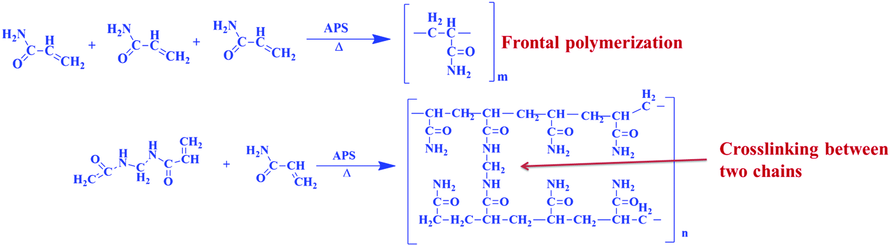
The WS2–polyacrylamide-based metallopolymer was synthesized by the thermo-frontal polymerization method. In this process, front polymerization was propagated in all the monomers in the polymer for a very short period. For obtaining the best polymer, adiabatic polymerization is very efficient but it is also dangerous under the worst conditions. But in the frontal polymerization process, an excessive exothermic reaction is used to increase the rate of the reaction. In some cases, frontal polymerization is carried out with an initiator such as metal nitrates of Mn(II), Co(II) Ni(II), and Zn(II) in composition with M(AAm)4(NO3)2(H2O).56
2.3 Synthesis of metal monomer composite (MMC)
WS2 nanosheets in different weight ratios were synthesized by adding WS2 nanosheets to the acrylamide monomer. With the weight ratios of 50%, 100%, and 200% of WS2 in the fixed amount of acrylamide, a metal monomer composite was formed and samples were labeled as Sample 1, Sample 2, and Sample 3. In each sample, 2 mM of the initiator ammonium peroxydisulphate [(NH4)2S2O8] was added. These composites were mixed properly by mechanical grinding. In this process, the monomer attaches to the metal part of WS2 nanosheets. After mixing the monomer, WS2, and the initiator, most probably, WS2 sheets attach to the oxygen molecule of acrylamide [CH2CHCONH2] through weak van der Waals forces. As we have mentioned previously, frontal polymerization was carried out in a reaction vessel. Thus, we make a pellet of the desired shape and size, which will fit in the reaction vessel.
2.4 Frontal polymerization of MMC
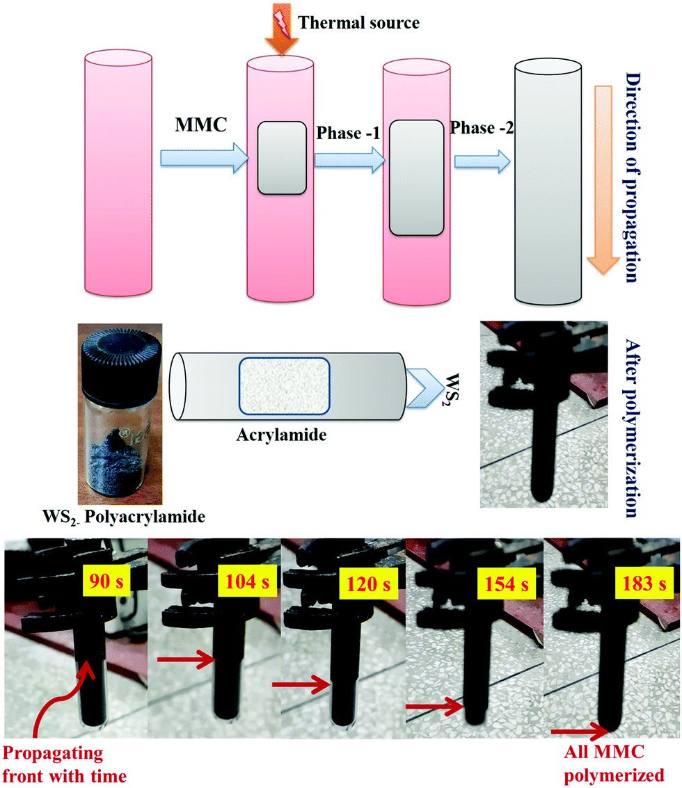
In frontal polymerization, acrylamide monomer is converted into polymer in a localized reaction zone. Frontal polymerization occurs in a definite arrangement with suitable thermo-physical properties, which are highly exothermic having a low heat conductivity coefficient. The heat generated during the polymerization of one monomer layer was used to activate the next monomer layer. The thermal wave proceeds in a narrow temperature range close to the adiabatic heating of the reaction medium. The possible reaction mechanism for the frontal polymerization is shown in Fig. 1 and the procedure of the frontal polymerization is depicted in Fig. 2.
 |
| | Fig. 1 Frontal polymerization reaction mechanism. | |
 |
| | Fig. 2 A synthesis procedure for the preparation of MOFs by frontal polymerization. | |
3. Results and discussion
3.1 Surface morphological and structural investigation
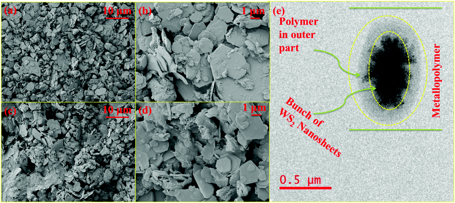
FE-SEM images of WS2 in the form of metallopolymer films exhibit large sheets in the dimension of tens of microns. The low magnification FE-SEM image of WS2 and metallopolymer show that these materials are made up of a large number of nanosheets and high-resolution FE-SEM shows that these nanosheets are roughly in the range of 150–300 nm with the thickness of around 10–20 nm as shown in Fig. 3. Big sheets of WS2 can be seen, but there is a large quantity of smaller sheets are also present. As seen in the TEM image, the inorganic WS2 content is incorporated in the polyacrylamide shell as depicted in Fig. 3e.
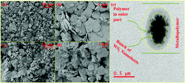 |
| | Fig. 3 Field emission scanning electron micrographs of (a) WS2 nanosheets at 10 μm scale (b) WS2 nanosheets at 1 μm scale (c) WS2–polyacrylamide at 10 μm scale (d) WS2–polyacrylamide at 1 μm scale (e) Tunneling electron micrograph of WS2–polyacrylamide at 0.5 μm scale. | |
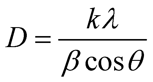
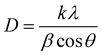
In the X-ray diffraction pattern of WS2 nanomaterial, (002), (004), (100), (103), (105), and (110) Bragg's planes are observed, which correspond to the 2θ angles of 14.42°, 28.86°, 32.96°, 39.46°, 49.68°, and 58.42°, respectively, as exhibited in Fig. 4a. In the pure polyacrylamide sample, a broad peak was found at 20.55°. This XRD pattern of WS2 confirms the 2H-phase belonging to the space group of P63/mmc. After the frontal polymerization, the hexagonal structure of the WS2 is not disturbed, as shown in the XRD diffractogram of the metallopolymeric samples. The calculated crystallite size of the WS2 is found to be 25.672 nm by the standard Debye–Scherrer formula as shown in eqn (1).
| |  | (1) |
where
λ is the CuK
α line wavelength of 0.154 nm,
β is FWHM and
k is the Scherrer constant.
57 In all metallopolymeric samples, such as 1, 2, and 3, crystalline peaks are found at the same positions as in the pure WS
2 sample. In sample 1, which contains more polyacrylamide than the other samples, a polyacrylamide peak is also found, whereas the amorphous peak of the polyacrylamide is suppressed in samples 2 and 3 because of the predominance of WS
2 in the metallopolymer.
 |
| | Fig. 4 (a) X-ray diffraction pattern (b) Differential scanning calorimetry (DSC) thermograms of the prepared samples 1, 2, and 3. | |
Differential scanning calorimetry is a technique to analyze the thermal properties of a sample under a controlled temperature. DSC analyses of all WS2–polyacrylamide samples were performed in the temperature region from 40 °C to 500 °C. The glass transition temperature of the metallopolymeric material is in the range of 70–110 °C as can be observed from Fig. 4b. After the glass transition temperature, the thermal vibrations in the sample begin. At the next stage, an endothermic peak was observed in the region of 277–331 °C. This peak is referred to as the melting of the metallopolymeric sample. On analyzing the melting points of samples 1, 2, and 3, it is noticeable that as the WS2 content increases the melting point also increases, which indicates the strong bonding between the polyacrylamide chain and WS2 nanomaterial.
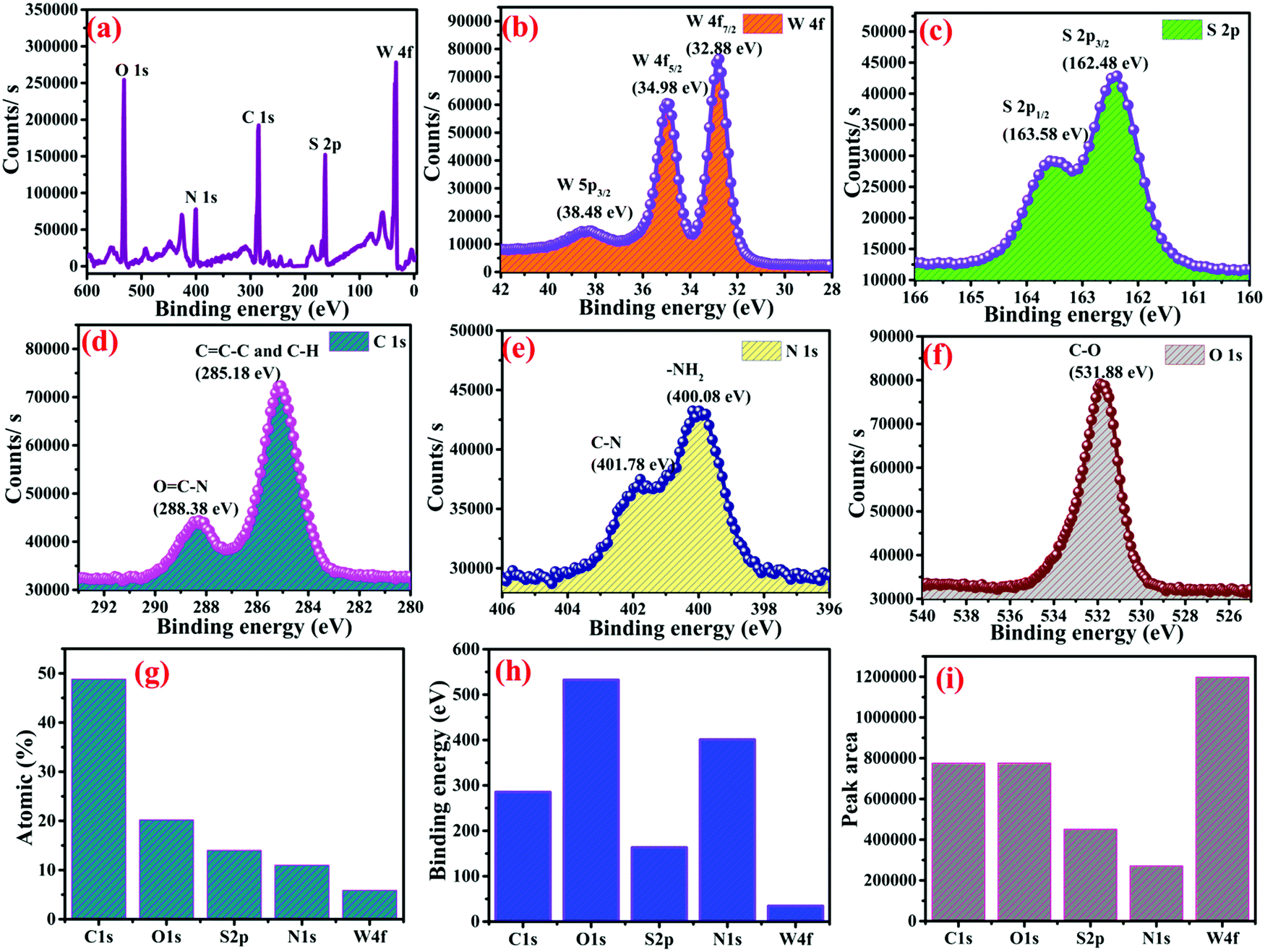
X-ray photoelectron spectroscopy (XPS) was used to study the species present in the WS2–polyacrylamide MOF. The XPS survey of WS2–polyacrylamide corresponding to their binding energies is presented in Fig. 5a, which confirmed the presence of elements W, S, C, N, and O. Their atomic weight percentages are shown in Fig. 5g. As seen from Fig. 5b, it is evident that tungsten possesses three distinct peaks with binding energies of 38.48 eV, 34.98 eV, and 32.88 eV, which correspond to the oxidation state of W 5p3/2, W 4f5/2, and W 4f7/2, respectively. The sulfur atoms exhibited two binding energy peaks, one for S 2p1/2 and the other for S 2p3/2, with the binding energies of 163.58 eV and 162.48 eV, respectively. The peak for O![[double bond, length as m-dash]](https://www.rsc.org/images/entities/char_e001.gif) C–N exhibited the binding energy of 288.38 eV and CC–C corresponds to the binding energy of 285.18 eV as shown in Fig. 5d, which are similar to those reported in the literature.58,59 The presence of nitrogen is also confirmed from the XPS spectra, as shown in Fig. 5e, with two distinct peaks one because of the C–N group and the other due to amide group nitrogen at the binding energies of 401.78 and 400.08 eV.59
C–N exhibited the binding energy of 288.38 eV and CC–C corresponds to the binding energy of 285.18 eV as shown in Fig. 5d, which are similar to those reported in the literature.58,59 The presence of nitrogen is also confirmed from the XPS spectra, as shown in Fig. 5e, with two distinct peaks one because of the C–N group and the other due to amide group nitrogen at the binding energies of 401.78 and 400.08 eV.59
 |
| | Fig. 5 (a) XPS spectra of WS2–polyacrylamide full scan (b) tungsten 5p and 4f (c) sulfur 2p (d) carbon 1s (e) nitrogen 1s (f) oxygen 1s (g) atomic weight percentage of elements (h) binding energy graph (i) peak area of the elements. | |
3.2 Optical approaches for investigation
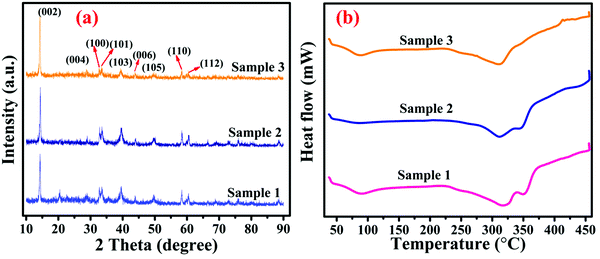
The presence of functional groups in WS2–polyacrylamide was analyzed using the FTIR spectra. In the FTIR spectra of the samples, various peaks are also observed. The peaks observed at 3424.9 cm−1 and 3178.1 cm−1 are attributed to the asymmetric and symmetric stretching vibrations of the –NH2 group. Asymmetric vibrations of the –CH2 functional group is around 2931.2 cm−1, as shown in Fig. 6a. The peak at 1662.3 cm−1 belongs to CO stretching vibration. C–N stretching vibrations and asymmetric vibrations of the C–C bond are observed at 1405.8 cm−1 and 1214.9 cm−1, respectively, as seen in Fig. S3 (ESI†). Bending vibrational peaks of –NH2 and W–S vibrational peaks are found at 1106.9 and 611.3 cm−1, respectively.
 |
| | Fig. 6 (a) Fourier transform infrared spectra (b) dynamic light scattering based particle size analysis (c) Raman spectra of the metallopolymeric samples (d) modes of vibrations in Raman spectra (e) absorbance spectra (f) Tauc plot for the bandgap analysis of the metallopolymer. | |
Various parameters, such as nanoparticle size, shape, surface charge, crystallinity, and functionalization with different ligands affect their electrical and optical properties. To analyze the distribution of the particle size, the DLS technique was used. In the DLS technique, laser light falls on the nanoparticles dispersed in the colloidal solution, and the intensity of the scattered light is detected. According to the DLS technique, each nanoparticle is considered spherical, but it is only a hypothesis, not a reality.60 Thus, the automated software averages the sizes of all the particles by assuming the hydrodynamic radius (RH) of all the particles as hard spheres, as in eqn (2). In this case, 2D materials show that they are found in the higher region of the particle size distribution. Stoke–Einstein relation is correlated with the hydrodynamic radius with an average diameter.
| |  | (2) |
where
kB is the Boltzmann constant,
T is the temperature at which measurements are carried out,
η is the absolute viscosity.
60,61 From
Fig. 6b, on analyzing samples 1, 2 and 3 we found that with a higher concentration of WS
2, the particle size distribution in the lower size diameter region. Most of the particles in sample 1 are distributed in the region of 550–950 nm; and in sample 2, this distribution is found in the region of 500–650 nm. But the nanoparticles in the highest WS
2 content sample 3 are distributed in the lowest region of the particle size of 350–600 nm.
In the Raman spectra of WS2–polyacrylamide samples, the displacements of the two Raman active modes are E12g and A1g. Where E12g mode shows in-plane displacement transition of W and S atoms; and in A1g mode, out of plane vibrations of the S atoms are involved, as shown in Fig. 6d. In the WS2 sample, E12g and A1g peaks are observed at 357.39 and 421.83 cm−1, whereas in all three samples such as 1, 2, and 3 no significant peak shifting is observed in comparison to the pure WS2 sample. In the metallopolymer samples 1, 2, and 3, as the percentage of polyacrylamide increases, the intensity of the peaks decreases.
Generally, the WS2 film exhibited strong photo-absorption in the whole UV to the visible range. Photodetectors based on WS2 nanomaterials show significant photoresponse in a very broad range of the solar spectrum. From Fig. 6e, in the UV-visible absorption spectra of metallopolymeric samples 1, 2, and 3, we found that the sample S3 (ESI†), which contained the higher WS2 content, exhibited the highest absorbance at 365 nm. At the wavelength of 365 nm, absorbance was found to be 29.79%, 54.63% and 80.34% for samples 1, 2, and 3, respectively. However, the absorbance spectra of all three samples are higher at long wavelengths. The bandgap of the materials is estimated from the Tauc plot using eqn (3).
where
α is the coefficient of absorption and m is an integer related to the type of transition.
62,63 The calculated bandgaps of the metallopolymeric samples are 4.590 eV, 4.40 eV, and 4.120 eV for metallopolymeric samples 1, 2, and 3, respectively, as shown in
Fig. 6f. It was observed that upon increasing the WS
2 content in the polyacrylamide matrix, the bandgap was reduced. By the analysis of the UV-visible spectra, it is observed that the optical properties of the MOFs can be controlled by the successive increasing or decreasing of the WS
2 content in the prepared samples. The sample with a minimum concentration of WS
2 shows the maximum transmission of greater than 80% for sample 1. On adding more WS
2, absorbance increases, thus the material is significant for photodetection. The main problem of these window layer materials may be low conductivity; and for higher conductivity, more WS
2 content must be incorporated, which reduces the transmittance. But this opens a door for researchers to make produce optically tunable materials. However, a higher conductivity is found under illumination and a lower dark current is suitable for minimizing the leakage current in the electronic devices.
64
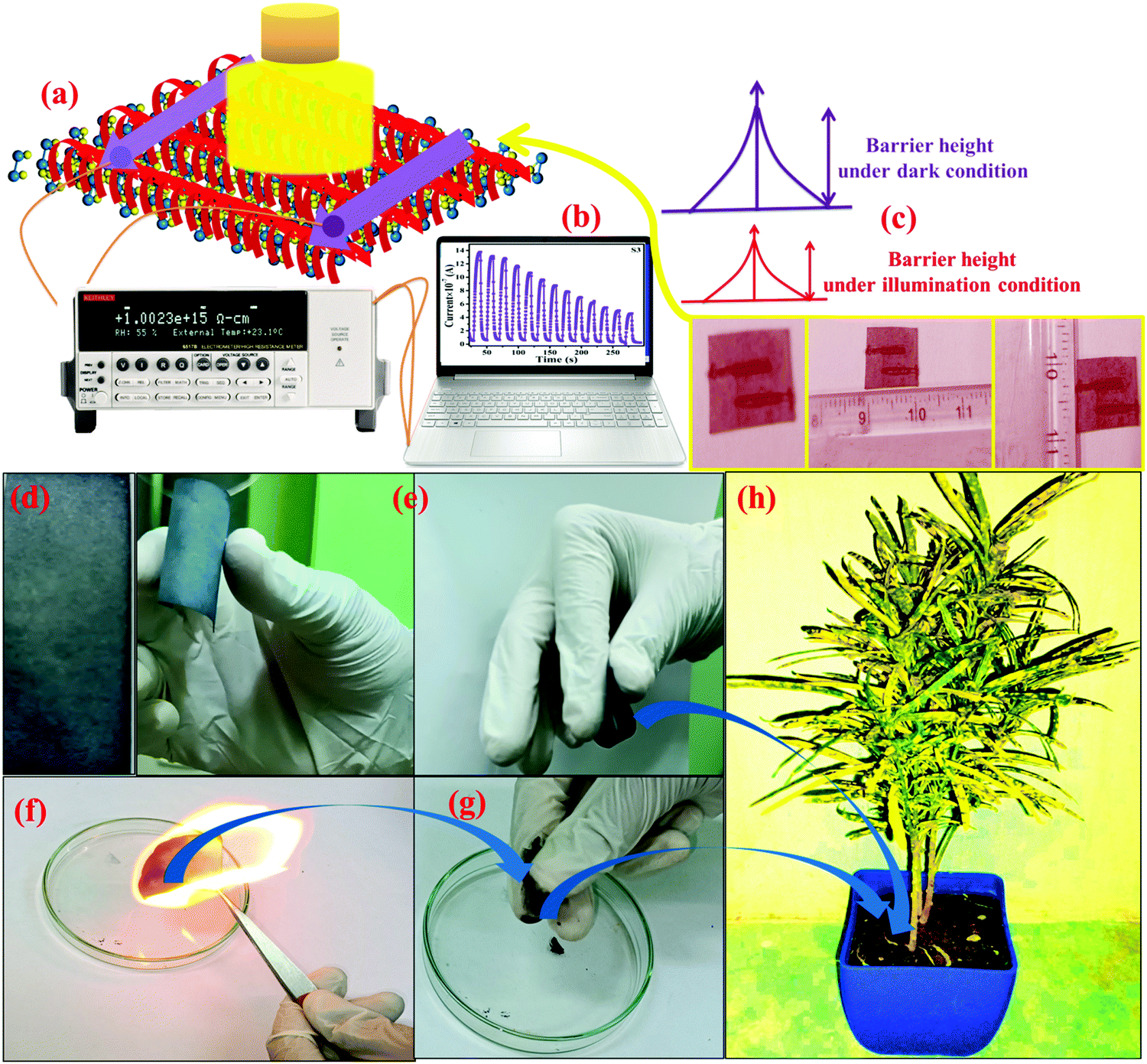
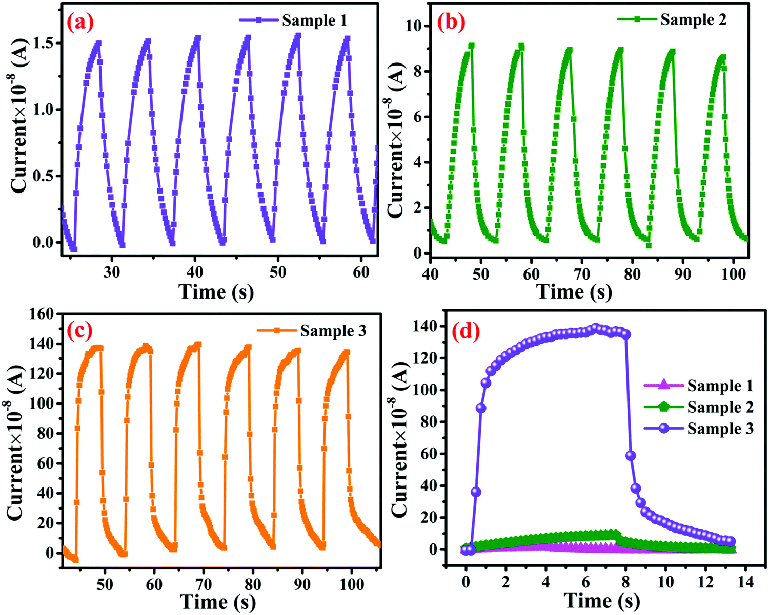
4. Photodetection mechanism and performance
The mechanism behind the photodetection is based on the chemisorption of oxygen molecules on the surface of the nanomaterial under the ambient atmospheric conditions in the form of O2− and creates a barrier between the material and adsorbed oxygen.65 Under the illumination condition, the barrier width between atmospheric oxygen and the metallopolymeric nanomaterial is reduced, as shown in Fig. 7a. Polyacrylamide induces a property in MOF-based photodetectors, which is the low threshold operating behavior of the devices. The current–voltage (I–V) studies were also performed in the range of −5 to 5 V under dark and illumination conditions. I–V characteristics of all samples are shown in the Fig. S4a–c (ESI†). Initial results suggest that the I–V characteristics are not pure Ohmic this is due to the fact that under illumination some space charge is generated and the temperature generated by illumination also plays a significant role in the I–V characteristics.32 This space charge behavior is significant in samples 1 and 3 but is improved in sample 3 due to the higher concentration of WS2 nanosheets incorporated in the polyacrylamide matrix. The transient photoresponse of samples 1, 2, and 3 are shown in Fig. 8a, b, and c, respectively, where their comparison in photocurrent is presented in Fig. 8d. The rate at which the carrier generation and recombination occur can be evaluated by the rise and decay time constants. The response and recovery time constants calculated by fitting the exponential rise and decay curves are presented in eqn (4) and (5), respectively.| | | I(t) = Idark(1 − e−t/τd) | (5) |
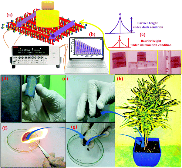 |
| | Fig. 7 (a) Photodetector device schematic diagram (b) data acquisition system (c) band diagram under dark and illumination (d) material coated on the paper substrate (e) flexibility of the device (f) burning of device (g) device degraded as biocompatible waste (h) final environment-friendly decomposition of photodetector device. | |
 |
| | Fig. 8 Transient photodetection of (a) sample 1 (b) sample 2 (c) sample 3 (d) photoresponse comparison of all three samples. | |
In the case of the response time, 10% to 90% rise in photocurrent, while for recovery time, 90% to 10% decay of photocurrent is considered. For sample 3, a fast rise time of 0.422 s and decay time of 0.543 s are found, as shown in Fig. 9d. This suggested that the sample, which contains a higher content of the polymers, exhibited lower time constants.
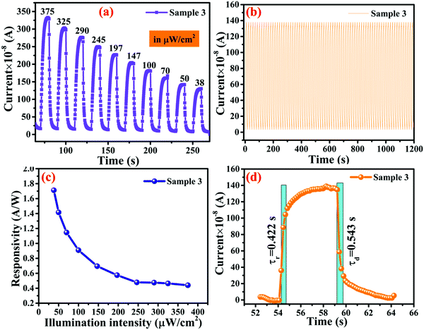 |
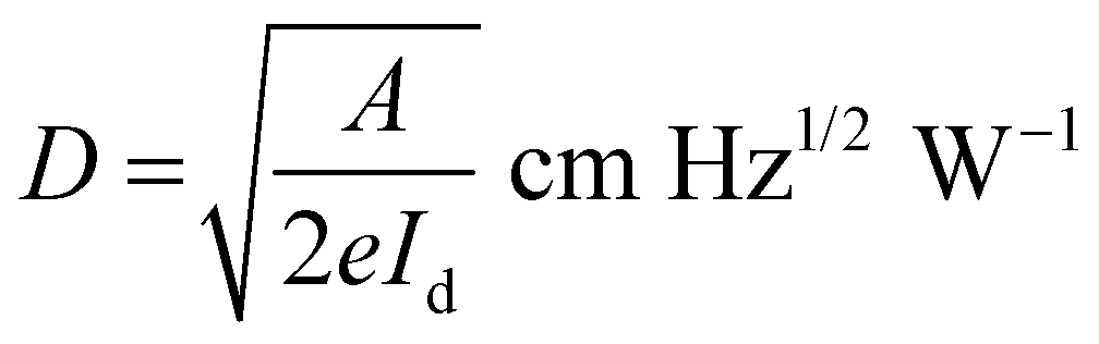
| | Fig. 9 (a) Transient photoresponse of sample 3 at different illumination intensities (b) stability of sample 3 over greater than 100 cycles (c) responsivity at different illumination intensities (d) rise and decay time for sample 3. | |
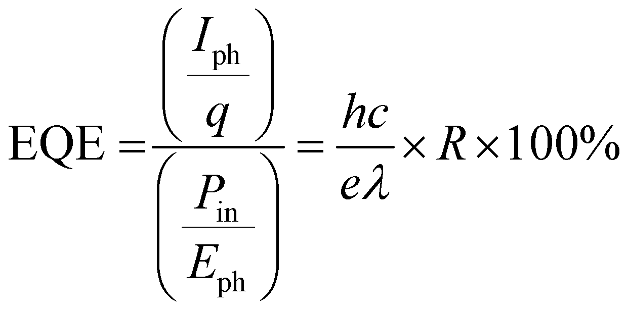
There are two significant parameters for analyzing the performance of the photodetector device, one is responsivity, and the other is external quantum efficiency, which are evaluated using eqn (6) and (7) respectively.
| | 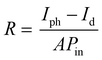 | (6) |
| |  | (7) |
where
Iph and
Id are the photo and dark currents.
A,
Pin and
λ are the exposure area, illumination intensity, and wavelength, respectively. For a unit exposure area and incident, optical power-generated photocurrent is termed as the responsivity.
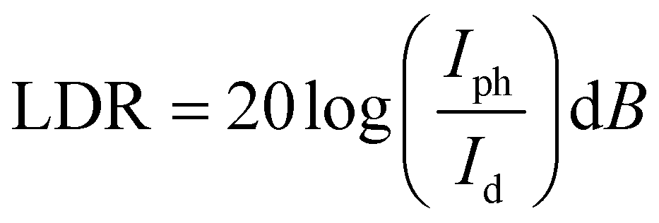
66,67 The external quantum efficiency (EQE) indicates the number of photoelectrons generated per photon. These two characteristics are linked to the efficiency with which a material turns an optical signal into electrical impulses. Thus, the quality of the carrier generation and separation of these excitons toward the electrodes are mainly described by the efficiency and responsivity. Responsivities of the MOF-based photodetectors are found to 0.001, 0.091, and 1.374 A W
−1 for samples 1, 2, and 3, respectively, which are also shown in
Fig. 10b. Wenbo Peng
et al. prepared a self-powered organic/inorganic PEDOT:PSS/ZnO based photodetector, which shows the responsivity of the 2.30 mA W
−1 for the 325 nm laser.
68 It was observed that on increasing the concentration of the WS
2 nanosheets, the conductivity of the materials was increasing, which is observed in terms of the responsivity. On the other hand carrier generations are also enhanced,
i.e., EQE of samples 1, 2, and 3 are observed as 0.599%, 31.069%, and 465.935%, respectively, at 365 nm. Higher than 100% excitons are not completely recombined in photoconductor-based photodetectors, but they do circulate several times in the external circuit, allowing for EQE. Different photodetectors with their photoresponse parameters based on various materials are given in
Table 1. Lei Lv
et al. reported an external quantum efficiency of 106% at 1122 nm for a polymeric photodetector.
69
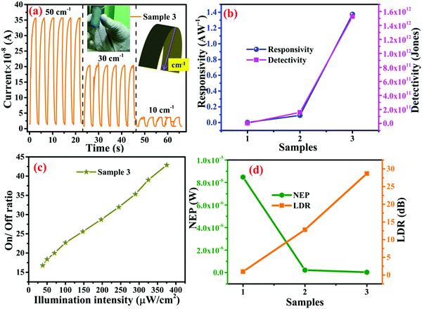 |
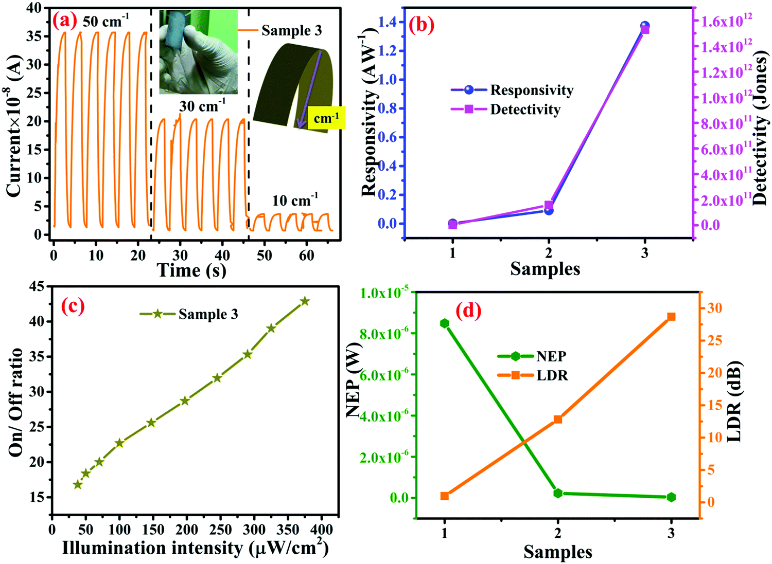
| | Fig. 10 Flexibility-dependent photoresponse at different curvatures at 50, 30 and 10 cm−1 (b) responsivity and detectivity of all samples (c) on–off ratio at different illumination intensities (d) Noise equivalent power and linear dynamic range of all samples. | |
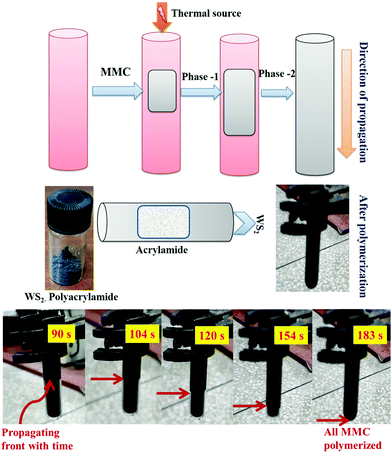
Other parameters, which are useful in analyzing the photodetector performance are the photo and dark current ratio (Ip/Id), noise equivalent power (NEP), detectivity (D), and linear dynamic range (LDR) were calculated and are presented in Table 2. These parameters largely depend on the dark current. The quantity linear dynamic range is the measurement of the incident light radiation over which, the photoresponse is linear.
| |  | (8) |
| |  | (9) |
A higher LDR means the photodetector can detect high light intensity signals as well as low signals.
70 In
Fig. 10d, sample 3 shows the highest LDR with a value of 28.6725 dB, and samples 1 and 2 exhibited LDR of 0.968 dB and 12.804 dB, respectively. Yuanzhi Wei
et al. designed a photodetector device based on the heterojunction, showing an LDR of 63 dB.
71 The noise equivalent power (NEP) is the amount of energy necessary to generate a certain noise current level. A comparative graph of NEP as in
Fig. 10d, in sample 3 (NEP = 3.6845 × 10
−8 W), minimum power is required to produce the photocurrent equal to dark current, which is much lower than the NEP values of sample 1 (NEP = 8.4799 × 10
−6 W) and sample 2 (NEP = 2.2897 × 10
−7W).
| |  | (10) |
Detectivity is defined to distinguish between the dark current and the photodetection capability of the device. It is reciprocal to the NEP normalized to the active area. This parameter is also used for the comparison of different geometries of the photodetectors.
72,73 The highest detectivity is observed for sample 3 based photodetector with the detectivity of 1.526 × 10
12 Jones. In samples 1 and 2, photodetector detectivity was observed as 3.608 × 10
9 and 1.581 × 10
11 Jones, respectively, as shown in
Fig. 10b. The TiO
2/MAPbI
3 quantum dot heterostructure-based photodetector device showed a similar detectivity of 3.8 × 10
11 Jones.
74
Table 2 The figure of merits of the photodetector device
| Samples |
Responsivity (A W−1) |
LDR (dB) |
EQE (%) |
Detectivity (Jones) |
NEP (W) |
| Sample 1 |
0.001 |
0.968 |
0.599 |
3.608 × 10⁹ |
8.479 × 10⁻⁶ |
| Sample 2 |
0.091 |
12.804 |
31.069 |
1.581 × 10¹¹ |
2.289 × 10⁻⁷ |
| Sample 3 |
1.374 |
28.672 |
465.935 |
1.526 × 10¹² |
3.684 × 10⁻⁸ |
For the analysis of the photoresponse of the flexible device under bending curvature, transient photoresponse was recorded under 50, 30, and 10 cm−1 bending curvature, and the bending curvature was measured using the method depicted in Fig. 10a (inset). At the maximum bending curvature of 50 cm−1, the photocurrent reduces from 140 × 10−8 A to 35 × 10−8 A, as presented in Fig. 10a. For samples 1 and 2, bending-based photoresponse measurements are shown in Fig. S5c and d (ESI†), respectively. As presented in the Table S3 (ESI†), at different bending curvatures, the photoresponse of the photodetector device changes. For sample 3, which contains maximum WS2 content, a maximum decrease in the photoresponsivity from 1.37428 A W−1 to 0.356 A W−1 was observed, which suggests that these MOFs are highly sensitive toward the bending curvature. As presented in Fig. 7f–h the disposability of the sample flame burning test and direct decomposition methods were used and it was observed that after burning the devices in the flame, the residue decomposes in a very short span of time; however, direct decomposition takes a longer time.
5. Conclusions
Frontal polymerized functional nanocomposites were investigated as low-cost, energy-efficient, biocompatible, flexible, and low threshold metal–organic frameworks (MOFs) for high performance photodetection. The synthesized MOFs with 2D WS2 improved the photodetection capability and enhanced their performance parameters. As can be seen from the preceding description, these 2D integrated polyacrylamide MOFs may prove to be an excellent choice for optoelectronic materials. From the photodetection analysis, the highest responsivity of 1.374 A W−1 with the detectivity of 1.5268 × 10¹² Jones was found. The linear dynamic range was found to be 28.672 dB. The photodetector parameters revealed that this material is very suitable for photodetection. The paper-based environmentally acceptable substrates may be employed to fabricate flexible photodetectors for commercial purposes in the near future.
Conflicts of interest
The authors declare that they have no known competing financial interests or personal relationships that could have appeared to influence the work reported in this paper.
Acknowledgements
Author Arpit Verma acknowledges Babasaheb Bhimrao Ambedkar University, Lucknow, U.P., India for providing UGC non-NET fellowship from 2018 to 2020. The authors are thankful to USIC, BBAU, Lucknow for providing XRD, FTIR facilities, BSIP, Lucknow for FE-SEM characterization, and CIF, Jiwaji University for providing TEM characterization facility. The authors are highly thankful to Advanced Materials Research Centre (AMRC) XPS Lab, IIT Mandi for providing the XPS facility.
References
- L. Zheng, P. Yu, K. Hu, F. Teng, H. Chen and X. Fang, ACS Appl. Mater. Interfaces, 2016, 8, 33924–33932 CrossRef CAS PubMed.
- D. Wu, J. Guo, J. Du, C. Xia, L. Zeng, Y. Tian, Z. Shi, Y. Tian, X. J. Li and Y. H. Tsang, ACS Nano, 2019, 13, 9907–9917 CrossRef CAS PubMed.
- V. K. Sangwan and M. C. Hersam, Annu. Rev. Phys. Chem., 2018, 69, 299–325 CrossRef CAS PubMed.
- M. Yu, D. Zhang, Y. Xu, J. Lin, C. Yu, Y. Fang, Z. Liu, Z. Guo, C. Tang and Y. Huang, J. Colloid Interface Sci., 2021, 608, 2367–2376 CrossRef.
- D. Wu, Z. Zhao, W. Lu, L. Rogée, L. Zeng, P. Lin, Z. Shi, Y. Tian, X. Li and Y. H. Tsang, Nano Res., 2021, 14, 1973–1979 CrossRef CAS.
- S. Kaushik, T. R. Naik, A. Alka, M. Garg, B. R. Tak, M. Ravikanth, V. R. Rao and R. Singh, ACS Appl. Electron. Mater., 2020, 2, 739–746 CrossRef CAS.
- K. Arora, K. Kaur and M. Kumar, ACS Appl. Electron. Mater., 2021, 3, 1852–1863 CrossRef CAS.
- R. Zhuo, L. Zeng, H. Yuan, D. Wu, Y. Wang, Z. Shi, T. Xu, Y. Tian, X. Li and Y. H. Tsang, Nano Res., 2019, 12, 183–189 CrossRef CAS.
- E. Wu, D. Wu, C. Jia, Y. Wang, H. Yuan, L. Zeng, T. Xu, Z. Shi, Y. Tian and X. Li, ACS Photonics, 2019, 6, 565–572 CrossRef CAS.
- M. Bernardi, M. Palummo and J. C. Grossman, Nano Lett., 2013, 13, 3664–3670 CrossRef CAS PubMed.
- A. Jager-Waldau, M. C. Lux-Steiner, E. Bucher and G. Jager-Waldau, IEEE Photovoltaic Specialists, 1993, 23, 597–602 Search PubMed.
- A. Splendiani, L. Sun, Y. Zhang, T. Li, J. Kim, C.-Y. Chim, G. Galli and F. Wang, Nano Lett., 2010, 10, 1271–1275 CrossRef CAS PubMed.
- Q. H. Wang, K. Kalantar-Zadeh, A. Kis, J. N. Coleman and M. S. Strano, Nat. Nanotechnol., 2012, 7, 699–712 CrossRef CAS PubMed.
- K. Kaur, K. Arora, B. Behzad, Q. Qiao and M. Kumar, Nanotechnology, 2018, 30, 065706 CrossRef PubMed.
- S. Kaushik and R. Singh, Adv. Opt. Mater., 2021, 2002214 CrossRef CAS.
- R. Wadhwa, A. V. Agrawal and M. Kumar, J. Phys. D: Appl. Phys., 2022, 55, 063002 CrossRef CAS.
- M. Akermi, N. Jaballah, I. M. Alarifi, M. Rahimi-Gorji, R. B. Chaabane, H. B. Ouada and M. Majdoub, J. Mol. Liq., 2019, 287, 110963 CrossRef CAS.
- Z. Liao, M. Ma, Z. Tong, R. Wang, Y. Bi, Y. Chen, K. L. Chung and Y. Ma, J. Colloid Interface Sci., 2021, 602, 602–611 CrossRef CAS PubMed.
- V. K. Singh, S. M. Yadav, H. Mishra, R. Kumar, R. S. Tiwari, A. Pandey and A. Srivastava, ACS Appl. Nano Mater., 2019, 2, 3934–3942 CrossRef CAS.
- X. Yang, Y. Liu, H. Lei and B. Li, Nanoscale, 2016, 8, 15529–15537 RSC.
- R. A. Talib, M. J. Abdullah, H. S. Al-Salman, S. M. Mohammad and N. K. Allam, Mater. Chem. Phys., 2016, 181, 7–11 CrossRef CAS.
- P. Li, F.-F. Cheng, W.-W. Xiong and Q. Zhang, Inorg. Chem. Front., 2018, 5, 2693–2708 RSC.
- A. Singh, S. Sikarwar, A. Verma and B. C. Yadav, Sens. Actuators, A, 2021, 113127 CrossRef CAS.
- K. Arora, N. Goel, M. Kumar and M. Kumar, ACS Photonics, 2018, 5, 2391–2401 CrossRef CAS.
- T. Zhu, Y. Yang, L. Zheng, L. Liu, M. L. Becker and X. Gong, Adv. Funct. Mater., 2020, 30, 1909487 CrossRef CAS.
- Y. Wang, L. Li, H. Wang, L. Su, H. Chen, W. Bian, J. Ma, B. Li, Z. Liu and A. Shen, Nanoscale, 2020, 12, 1406–1413 RSC.
- S. Rajamani, K. Arora, A. Konakov, A. Belov, D. Korolev, A. Nikolskaya, A. Mikhaylov, S. Surodin, R. Kryukov and D. Nikolitchev, Nanotechnology, 2018, 29, 305603 CrossRef.
- P. Yu, K. Hu, H. Chen, L. Zheng and X. Fang, Adv. Funct. Mater., 2017, 27, 1703166 CrossRef.
- T.-H. Tsai, A. K. Sahoo, H.-K. Syu, Y.-C. Wu, M.-Y. Tsai, M.-D. Siao, Y.-C. Yang, Y.-F. Lin, R.-S. Liu and P.-W. Chiu, ACS Appl. Electron. Mater., 2021, 3, 4291–4299 CrossRef CAS.
- Z. Zhao, D. Wu, J. Guo, E. Wu, C. Jia, Z. Shi, Y. Tian, X. Li and Y. Tian, J. Mater. Chem. C, 2019, 7, 12121–12126 RSC.
- P. Chaudhary, A. Verma, A. Mishra, D. Yadav, K. Pal, B. C. Yadav, E. R. Kumar, K. B. Thapa, S. Mishra and D. K. Dwivedi, Phys. E, 2022, 139, 115174 CrossRef.
- A. Verma, P. Chaudhary, R. K. Tripathi and B. C. Yadav, Sustainable Energy Fuels, 2021, 5, 1394–1405 RSC.
- Z. Duan, J. Ning, M. Chen, Y. Xiong, W. Yang, F. Xiao, S. V. Kershaw, N. Zhao, S. Xiao and A. L. Rogach, ACS Appl. Mater. Interfaces, 2020, 12, 35201–35210 CrossRef CAS.
- D. Guo, D. Yang, J. Zhao, A. Vadim and D. Ma, J. Mater. Chem. C, 2020, 8, 9024–9031 RSC.
- X. Wang, W. Song, B. Liu, G. Chen, D. Chen, C. Zhou and G. Shen, Adv. Funct. Mater., 2013, 23, 1202–1209 CrossRef CAS.
- E. Goli, T. Gai and P. H. Geubelle, J. Phys. Chem. B, 2020, 124, 6404–6411 CrossRef CAS PubMed.
- L. K. Gupta, K. Kumar, B. C. Yadav, T. P. Yadav, G. I. Dzhardimalieva and I. E. Uflyand, Sens. Actuators, A, 2021, 112839 CrossRef CAS.
- J. A. Pojman, ACS Cent. Sci., 2021, 7, 534–535 CrossRef.
- I. D. Robertson, M. Yourdkhani, P. J. Centellas, J. E. Aw, D. G. Ivanoff, E. Goli, E. M. Lloyd, L. M. Dean, N. R. Sottos and P. H. Geubelle, Nature, 2018, 557, 223–227 CrossRef CAS PubMed.
- P. Chaudhary, D. K. Maurya, R. K. Tripathi, B. C. Yadav, N. D. Golubeva, E. I. Knerelman, I. E. Uflyand and G. I. Dzhardimalieva, Mater. Adv., 2020, 1, 2804–2817 RSC.
- S. Sorifi, M. Moun, S. Kaushik and R. Singh, ACS Appl. Electron. Mater., 2020, 2, 670–676 CrossRef CAS.
- A. Verma, P. Chaudhary, R. K. Tripathi and B. C. Yadav, Sens. Actuators, A, 2021, 321, 112600 CrossRef CAS.
- Y. Xin, X. Wang, Z. Chen, D. Weller, Y. Wang, L. Shi, X. Ma, C. Ding, W. Li and S. Guo, ACS Appl. Mater. Interfaces, 2020, 12, 15406–15413 CrossRef CAS PubMed.
- F. Yan, L. Zhao, A. Patanè, P. Hu, X. Wei, W. Luo, D. Zhang, Q. Lv, Q. Feng and C. Shen, Nanotechnology, 2017, 28, 27LT01 CrossRef PubMed.
- D. Kannichankandy, P. M. Pataniya, C. K. Zankat, M. Tannarana, V. M. Pathak, G. K. Solanki and K. D. Patel, Appl. Surf. Sci., 2020, 524, 146589 CrossRef CAS.
- D. Nath, P. Dey, A. M. Joseph, J. K. Rakshit and J. N. Roy, Opt. Mater., 2020, 108, 110371 CrossRef CAS.
- D. Nath, P. Dey, A. M. Joseph, J. K. Rakshit and J. N. Roy, Opt. Laser Technol., 2020, 131, 106393 CrossRef CAS.
- S.-W. Lee, K.-J. Choi, B.-H. Kang, J.-S. Lee, S.-W. Kim, J.-B. Kwon, S.-A. Gopalan, J.-H. Bae, E.-S. Kim and D.-H. Kwon, Org. Electron., 2016, 39, 250–257 CrossRef CAS.
- R. A. Talib, M. Abdullah, H. S. Al-Salman, S. M. Mohammad and N. K. Allam, Mater. Chem. Phys., 2016, 181, 7–11 CrossRef CAS.
- Y.n. Ji, N. Wang, N. Ding, W. Xu, H. Song and D. Zhou, J. Rare Earths, 2022, 40, 211–217 CrossRef CAS.
- M. Zhu, Z. Zhao, Y. Fang, C. Fang, Z. Weng, W. Lei, S. B. Shafie and M. N. Mohtar, Appl. Phys. A: Mater. Sci. Process., 2021, 127, 1–8 CrossRef.
- D. Wu, J. Guo, C. Wang, X. Ren, Y. Chen, P. Lin, L. Zeng, Z. Shi, X. J. Li and C.-X. Shan, ACS Nano, 2021, 15, 10119–10129 CrossRef PubMed.
- D. Wu, C. Guo, Z. Wang, X. Ren, Y. Tian, Z. Shi, P. Lin, Y. Tian, Y. Chen and X. Li, Nanoscale, 2021, 13, 13550–13557 RSC.
- Z. Wang, X. Zhang, D. Wu, J. Guo, Z. Zhao, Z. Shi, Y. Tian, X. Huang and X. Li, J. Mater. Chem. C, 2020, 8, 6877–6882 RSC.
- C. Jia, X. Huang, D. Wu, Y. Tian, J. Guo, Z. Zhao, Z. Shi, Y. Tian, J. Jie and X. Li, Nanoscale, 2020, 12, 4435–4444 RSC.
- V. S. Savostyanov, D. A. Kritskaya, A. N. Ponomarev and A. D. Pomogailo, J. Polym. Sci., Part A: Polym. Chem., 1994, 32, 1201–1212 CrossRef CAS.
- A. Singh and P. Chauhan, Mater. Today: Proc., 2020, 46, 6264–6269 Search PubMed.
- P. Chaudhary, D. K. Maurya, A. Pandey, A. Verma, R. K. Tripathi, S. Kumar and B. C. Yadav, Sens. Actuators, B, 2021, 130818 Search PubMed.
- G. Zorn, L.-H. Liu, L. Árnadóttir, H. Wang, L. J. Gamble, D. G. Castner and M. Yan, J. Phys. Chem. C, 2014, 118, 376–383 CrossRef CAS PubMed.
- S. Bhattacharjee, J. Controlled Release, 2016, 235, 337–351 CrossRef CAS PubMed.
- U. Kumar and B. C. Yadav, Sens. Actuators, B, 2019, 288, 399–407 CrossRef CAS.
- S. Mishra, P. Lohia, P. Chaudhary, B. C. Yadav and D. K. Dwivedi, J. Electron. Mater., 2020, 49, 6492–6500 CrossRef CAS.
- A. Singh, S. Sikarwar and B. C. Yadav, Mater. Res. Express, 2021, 8, 045013 CrossRef CAS.
-
Z. J. Chen, K. Y. Ling, H. Shichijo, K. Komatsuzaki and C.-Y. Tsai, US Pat. 6621064, 2003.
- M. Patel, P. M. Pataniya, D. J. Late and C. K. Sumesh, Appl. Surf. Sci., 2021, 538, 148121 CrossRef CAS.
- R. K. Tripathi, O. S. Panwar, I. Rawal, C. K. Dixit, A. Verma, P. Chaudhary, A. K. Srivastava and B. C. Yadav, J. Mater. Sci.: Mater. Electron., 2021, 32, 2535–2546 CrossRef CAS.
- C. Gautam, A. Verma, P. Chaudhary and B. C. Yadav, Opt. Mater., 2022, 123, 111860 CrossRef.
- W. Peng, X. Wang, R. Yu, Y. Dai, H. Zou, A. C. Wang, Y. He and Z. L. Wang, Adv. Mater., 2017, 29, 1606698 CrossRef PubMed.
- L. Lv, W. Dang, X. Wu, H. Chen, T. Wang, L. Qin, Z. Wei, K. Zhang, G. Shen and H. Huang, Macromolecules, 2020, 53, 10636–10643 CrossRef CAS.
- S. Singh, A. Bhaduri, R. K. Tripathi, K. B. Thapa, R. Kumar and B. C. Yadav, Sol. Energy, 2019, 188, 278–290 CrossRef CAS.
- Y. Wei, G. Feng, P. Mao, Y. Luan, J. Zhuang, N. Chen, H. Yang, W. Li, S. Yang and J. Wang, ACS Appl. Mater. Interfaces, 2020, 12, 8826–8834 CrossRef CAS PubMed.
- T. Huo, H. Yin, D. Zhou, L. Sun, T. Tian, H. Wei, N. Hu, Z. Yang, Y. Zhang and Y. Su, ACS Sustainable Chem. Eng., 2020, 8, 15532–15539 CrossRef CAS.
- R. K. Chowdhury, T. K. Sinha, A. K. Katiyar and S. K. Ray, Nanoscale, 2017, 9, 15591–15597 RSC.
- Z. Zheng, F. Zhuge, Y. Wang, J. Zhang, L. Gan, X. Zhou, H. Li and T. Zhai, Adv. Funct. Mater., 2017, 27, 1703115 CrossRef.
Footnote |
| † Electronic supplementary information (ESI) available: Supporting information contains characterization tools, photodetector device fabrication method, structural analysis, extra information of FTIR spectra of sample S3, conduction mechanism of the device, photodetector parameters comparison table, current–voltage characteristics of all the samples, rise and decay time constant fitting of sample 1 and 2, graph between photocurrent and illumination intensity, stability of the photodetector device for sample 1 and 2 over more than 100 cycles, bending based photoresponse characteristics of samples 1 and 2 at the bending curvature of 50, 30 and 10 cm−1, bending dependent photoresponse parameters, scanning electron micrograph of carbon nanotube-based electrode material. See DOI: 10.1039/d2ma00023g |
|
| This journal is © The Royal Society of Chemistry 2022 |
Click here to see how this site uses Cookies. View our privacy policy here. 
 Open Access Article
 This Open Access Article is licensed under a
  a,
Priyanka
Chaudhary
a,
Priyanka
Chaudhary