
 Open Access Article
 This Open Access Article is licensed under a
 Creative Commons Attribution 3.0 Unported Licence
Honeycomb-structured copper indium sulfide thin films obtained via a nanosphere colloidal lithography method†
Efthymia
Vakalopoulou
 a,
Thomas
Rath
*a,
Fernando Gustavo
Warchomicka
b,
Francesco
Carraro
c,
Paolo
Falcaro
c,
Heinz
Amenitsch
d and
Gregor
Trimmel
a
a,
Thomas
Rath
*a,
Fernando Gustavo
Warchomicka
b,
Francesco
Carraro
c,
Paolo
Falcaro
c,
Heinz
Amenitsch
d and
Gregor
Trimmel
a
aInstitute for Chemistry and Technology of Materials, NAWI Graz, Graz University of Technology, Stremayrgasse 9, 8010 Graz, Austria. E-mail: thomas.rath@tugraz.at
bInstitute of Materials Science, Joining and Forming, Graz University of Technology, Kopernikusgasse 24, 8010, Graz, Austria
cInstitute of Physical and Theoretical Chemistry, NAWI Graz, Graz University of Technology, Stremayrgasse 9, 8010 Graz, Austria
dInstitute of Inorganic Chemistry, NAWI Graz, Graz University of Technology, Stremayrgasse 9, 8010 Graz, Austria
First published on 24th February 2022
Abstract
The large surface-to-volume ratio and the huge surface area of an ordered nanostructure is essential for improving the performance of many metal sulfide-based technologies within energy conversion and storage, but also catalysis and sensing. Although, several routes toward the formation of nanostructured metal sulfide thin films have been already developed, their fabrication is still challenging. Herein, we present a novel method for the preparation of honeycomb-structured CuInS2 thin films via a nanosphere colloidal lithography technique using monodisperse polystyrene nanosphere layers, formed by a self-assembly approach at the air/liquid interface, as template. The size of the spheres can be reduced by an O2 plasma etching process, thereby enlarging the free space between the spheres. Infiltration of the template with metal xanthates followed by their thermal conversion to CuInS2 and the thermal removal of the polymeric template leads to ordered honeycomb-structured films. In an alternative route, the template is infiltrated with a tailored CuInS2 nanoparticle ink before the template is removed by dissolution.
Introduction
In the past few years, ordered nanostructured materials gained increasing interest in optoelectronics, sensors, but also in energy related applications including batteries, capacitors, solar cells and in particular catalytic CO2 reduction, or hydrogen production.1,2 For the formation of ordered nanostructured materials, metal oxides, siliceous and carbon based materials are prevalent among the research community. The reason for this pre-eminence is mainly the huge amount of suitable precursors and their ability to take part in sol–gel reactions.3 In contrast, due to their less controlled sol–gel processes and sensitivity towards experimental conditions, reports about routes towards ordered nanostructured films of sulfides, selenides, carbides and nitrides are scarce.3 Especially metal sulfides, widely used in applications such as energy conversion and storage, catalysis and water splitting,4,5 can benefit from the formation of ordered nanostructures as the large surface-to-volume ratio of the structured materials can be a key point for further improving their performance in these above mentioned applications.6The major structuring techniques are based on templates. There are two templating strategies, namely hard-templating or nanocasting routes, and soft-templating. The first route employs usually a hard exotemplate, such as mesoporous silica,7 whereas the second uses structure directing agents, such as liquid crystals.8 Both techniques face several limitations. In the case of the soft-templating route, in contrast to the metal oxides, which can be easily formed via oxidation of metal-based compounds at elevated temperatures under ambient atmosphere, the metal sulfide formation requires, in most of the cases, two precursor materials: one that provides the metal ion and the other providing the sulfur ion. However, the coexistence of the two precursors and their high reactivity, immediately leads to the metal sulfide precipitation and uncontrolled growth. As a result, the precursors do not have the time to interact with the structure directing agent. Additionally, the experimental conditions, such as temperature and pH values, which are needed for the self-assembly of the soft-template are typically different to the ones needed for the crystallization of the metal sulfide.9,10 In case of the nanocasting route, even though the exotemplate is not influenced by the conditions needed for the formation of the metal sulfides, as they are produced at an earlier step and it can be stable at very high temperatures, the main problem lies on the use of hazardous chemicals (e.g. HF) for its removal.7 Lastly, a general challenge regarding the preparation of structured metal sulfide layers is due to the used precursor materials (e.g. metal salts and a sulfur source, or single source precursors) and their shrinkage in volume during the conversion, which can be up to 90%.10,11 This issue leads to the need of numerous repetitions of the infiltration and conversion steps until the desired result is obtained or a loss of the interconnected porous structure causing a decrease of the accessible surface area.
Apart from the templating route, other techniques were introduced for the formation of ordered nanostructured metal sulfide thin films, such as UV-light lithography, which is performed with the aid of metal xanthate precursors acting as negative resist.12 Metal xanthates are metal organic compounds with a typical metal–sulfur bond, which can decompose at elevated temperatures or in certain conditions also at room temperature resulting into metal sulfides and are therefore considered as single-source precursors.13,14 An alternative to UV lithography is the e-beam lithography, where suitable single source precursors, such as metal thiolates or xanthates, as well as long-chain metal anion-alkyl ammonium complexes15 are lithographically patterned for the formation of structured metal sulfides. Both UV and e-beam lithography techniques do not use all the typical steps of a conventional lithography, but only the exposure, which converts the soluble precursor to the insoluble metal sulfide and subsequently the development, which removes the precursor via a dissolution in a common solvent, such as chloroform. These lithographic techniques have the disadvantages of low throughput, high costs and time-consuming preparation of the templates.
Another method for the formation of patterned metal sulfide microarrays is via self-assembled monolayers (SAMs) as functional organic templates.16 SAMs are patterned usually via UV-lithography, which results in the formation of different functionalities and subsequently can induce the adsorption and crystallization of the metal sulfides only in desired positions. A less known technique is the micromolding in capillaries (MIMIC).17 The technique employs an elastomeric stamp which is placed on the substrate. A small amount of the precursor solution is positioned at the end of the stamp and due to capillary forces, the micromold is filled. Drying and post-treatment steps follow, resulting into patterned structures. Nevertheless, the complex fabrication protocol makes the latter techniques cumbersome structuring routes.
An alternative method overcoming several of the aforementioned limitations is the nanosphere colloidal lithography.18 This type of lithography, also referred to as natural lithography,19 is a patterning method, where colloidal monodispersed particles are self-assembled and used as a template for the production of periodically ordered arrays. Compared to the common lithography techniques, nanosphere colloidal lithography is also highly reproducible and controllable, however, as no special equipment is necessary, it is simpler and less expensive. Additionally, the structure size can range from tens of nanometers up to several micrometers. At the moment, popular colloidal particles are silica and polymer spheres, such as polystyrene (PS) and poly(methyl methacrylate) (PMMA).20 The spheres are assembled into hexagonally structured arrays via several methods, such as drop-, dip- and spin-coating, electrophoretic deposition and self-assembly at the gas/liquid interface.21 Hence, the hexagonally structured spheres can be used as templates, known also as opal, where the desired materials are infiltrated in the interstitial space of the spheres. Subsequently, the template is removed, resulting into the negative architecture of the material, also known as inverse opal (IO). In the literature, there are numerous studies that employ the nanosphere colloidal lithography to form hexagonally structured thin films. However, these reports focus on the syntheses of inorganic materials, such as the oxides TiO2,22,23 SiO2,23,24 In2O3,25 ITO26 and organometal halide perovskites,27 as well as Ag,28 Ni–P.29
In this study, we present the preparation of honeycomb-structured CuInS2 thin films via two colloidal nanosphere lithography approaches. CuInS2 is a well-studied, non-toxic, ternary metal sulfide material30 and macroporous structured CuInS2 films are of high interest in applications such as (photo)catalysis for water splitting5 and inorganic–organic heterojunction solar cells.2,34 Regarding the solution-based formation of CuInS2 thin films, there are several studies focusing on either salts precursors31 or metal xanthates.32,33 Here, in the first investigated colloidal lithography route, a direct infiltration of a precursor solution containing copper and indium xanthates and an in situ thermal conversion to the metal sulfide is applied. In the second route, novel thioglycerol-capped CuInS2 nanocrystals (NCs) were synthesised, characterized and employed for the formation of honeycomb-structured thin films.
Results and discussion
a. Formation and characterization of the PS-NS templates
The polystyrene nanosphere (PS-NS) templates were prepared with an air/liquid interface method using a suspension of the PS-NS in a water/ethanol mixture. The overall preparation process is illustrated in Fig. 1. A glass slide is placed in the centre of a Petri dish, an amount of the suspension is dropped on the glass slide and subsequently water is slowly added until the PS suspension is rapidly spread on the air/water interface, leading to the two-dimensional (2D) layer assembly. Upon the formation of the layer, a blueish structural colour appeared at the air/liquid interface, generated when the incident light on the ordered structure undergoes diffraction and the wavelength of the reflected light fulfils the Bragg's conditions.35 Subsequently, the transfer of the PS-NS arrays on the substrates (silicon wafer) was performed by inserting the substrates below the layer and lifting them from the interface. Finally, the PS-NS templates immobilized on the substrates were dried under ambient conditions. In Fig. 1(b) and Fig. S1 (ESI†), the SEM images of the closely-packed PS-NS arrays on the substrate are depicted, with the sphere diameter being 264 ± 20 nm.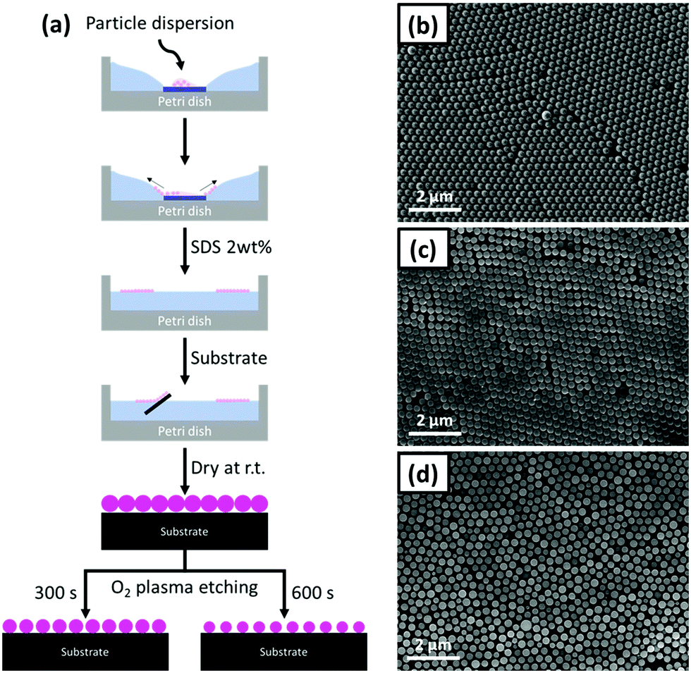 | ||
| Fig. 1 (a) Schematic illustration of the overall preparation process of the PS-NS templates. SEM images of (b) P0, (c) P300 and (d) P600 PS-NS templates. | ||
However, the 2D hexagonal packing of the nanospheres was so tight that the interstitial space was insufficient for the formation of stable walls made of the infiltrated material. Thus, the PS-NS templates were modified by O2 plasma etching. This leads to a size reduction of the spheres and consequently to an interstitial space increase between the spheres. The O2 plasma etching is an isotropic process, meaning that it is performed not only on the surface but also into existing cavities.36 As a result, the size of the spheres was homogeneously reduced depending on the etching durations. In our work, we operated an O2 plasma etching for 300 and 600 s. The diameter after 300 s was at approx. 236 nm, whereas after 600 s it was further reduced to 206 nm. In the following, the different PS-NS templates are referred to as Px (x = 0, 300, 600 depending on the O2 plasma etching duration). In Fig. 1(b–d), the SEM images of P0, P300 and P600 are presented.
After the successful preparation of the templates, we investigated two solution-based approaches to incorporate the metal sulfide, which are schematically illustrated in Fig. 2. In the first route, a solution containing a mixture of copper and indium xanthates was infiltrated into the nanostructure followed by an in situ thermal conversion to the metal sulfide. In the second route, an ink containing pre-synthesized thioglycerol-capped CuInS2 NCs was employed for the infiltration. The PS nanospheres were removed from the film either by a thermal decomposition process or dissolution to obtain the honeycomb-structured thin films of CuInS2.
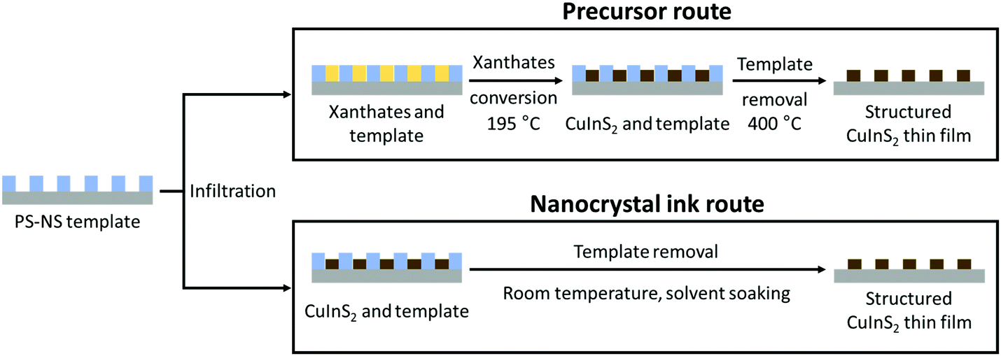 | ||
| Fig. 2 Schematic presentation of the two PS-NS template routes based on (i) precursor infiltration/conversion and (ii) nanocrystal ink infiltration for the formation of honeycomb structured CuInS2 thin films. | ||
b. Formation of honeycomb-structured films via in situ CuInS2 production – precursor route
In this approach, the PS-NS template is infiltrated with a CuInS2 precursor solution consisting of a mixture of copper and indium xanthates (copper O-2,2-dimethylpentan-3-yl dithiocarbonate and indium O-2,2-dimethylpentan-3-yl dithiocarbonate).33 The challenge hereby is that these compounds are highly soluble in solvents such as chloroform and toluene, which also dissolve polystyrene. Consequently, polar solvents, such as ethanol, used in the formation of hexagonally-structured TiO2 and SiO2 with PS-NS templates, would be beneficial.23,24 However, ethanol does not dissolve the metal xanthates (in particular the copper xanthate shows very low solubility in polar solvents) and hence, according to a previous study, a solvent mixture of ethanol![[thin space (1/6-em)]](https://www.rsc.org/images/entities/char_2009.gif) :dichloromethane:ethanolamine (20:10:1, vol. ratio) was used, in order to form a clear and stable precursor solution, while it does not dissolve the polystyrene template.37 The infiltration was realized by drop casting the solution onto the template film and soaking for several seconds followed by spinning off the excess amount of solution at a speed of 5000 rpm using a spin coater. This assures a good infiltration of the template, without the formation of a noticeable continuous precursor film on top of the template.
:dichloromethane:ethanolamine (20:10:1, vol. ratio) was used, in order to form a clear and stable precursor solution, while it does not dissolve the polystyrene template.37 The infiltration was realized by drop casting the solution onto the template film and soaking for several seconds followed by spinning off the excess amount of solution at a speed of 5000 rpm using a spin coater. This assures a good infiltration of the template, without the formation of a noticeable continuous precursor film on top of the template.
After this step, the FT-IR spectrum (Fig. 3a) shows the vibrations of both the xanthates and the polystyrene, indicating that the infiltration procedure does not remove the template. Most of the vibration peaks appearing in the spectrum correspond to the xanthates. The high intensity peak at 2968 cm−1 correspond to the C–H asymmetric stretching vibration, while the peaks at 1240 and 1214 cm−1 and at 1056 and at 1036 cm−1 correspond to asymmetric C–O–C, C–S and C–H stretching vibrations of the xanthates, respectively.38 Regarding the polystyrene, lower intensity vibrations, which stem from an aromatic C–H stretching vibration, can be observed at 3025 cm−1. The bands at 1601, 1493 and 1452 cm−1 correspond to aromatic C![[double bond, length as m-dash]](https://www.rsc.org/images/entities/char_e001.gif) C stretching vibrations and the ones at 757 and 697 cm−1 to C–H out-of-plane bending vibrations.39
C stretching vibrations and the ones at 757 and 697 cm−1 to C–H out-of-plane bending vibrations.39
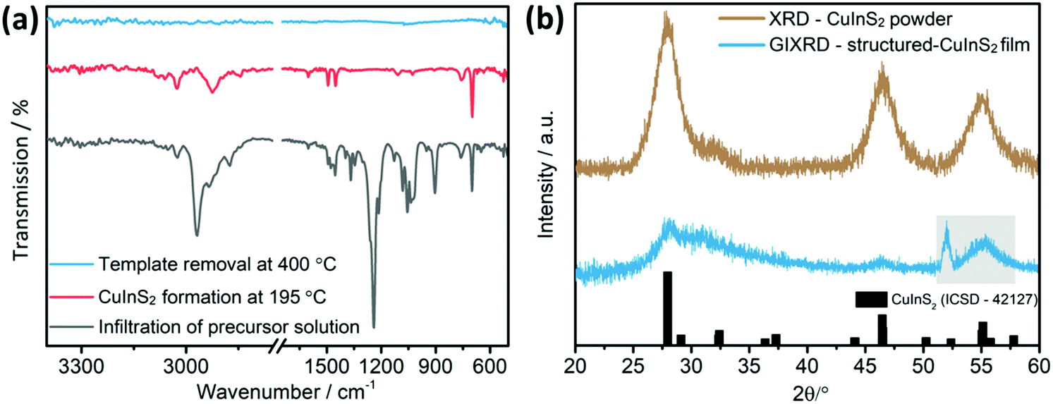 | ||
| Fig. 3 (a) FT-IR spectra after infiltration of the PS-NS template with the precursor solution (grey), after CuInS2 formation at 195 °C (red) and after template removal via thermal decomposition at 400 °C (blue). (b) Powder X-ray diffraction (PXRD, brown) and grazing incidence X-ray diffraction (GIXRD, blue) patterns of the CuInS2 powder and the structured CuInS2 film on a silicon substrate, respectively, obtained by decomposition of the xanthate precursors at 400 °C with a reference pattern for the chalcopyrite CuInS2 structure (ICSD-42127). The grey frame on the GIXRD pattern indicates the silicon diffraction peaks stemming from the substrate. The IR spectra and diffraction patterns are shifted vertically for better visibility. | ||
Subsequently, the metal xanthates are converted to copper indium sulfide by heating the samples to 195 °C under nitrogen atmosphere. The FT-IR spectrum of a sample heated to 195 °C does not reveal any vibration peaks related to the xanthates. All the peaks refer to polystyrene. Some were already mentioned before, while the ones at 2925 and 2843 cm−1 were superimposed by the high intensity xanthate peaks in the aforementioned spectrum.39 These vibration peaks correspond to the methylene group of polystyrene. Finally, the decomposition of polystyrene was accomplished at 400 °C under nitrogen. The corresponding FT-IR-spectrum does not show any vibrations in the range from 4000–400 cm−1, as all the organic material has been removed from the film.
A grazing incidence X-ray diffraction (GIXRD) measurement on the final film exhibits three broad diffraction peaks with low intensity at 28.1, 31.2 and 46.4° 2θ indicating the formation of chalcopyrite CuInS2 (Fig. 3b). To confirm this result, we analysed CuInS2 powder prepared with a very similar procedure, with the only difference that the precursor solution was placed in a glass container, dried and annealed at 400 °C under nitrogen atmosphere to yield a higher amount of material. The obtained pattern exhibits also the typical diffraction peaks of CuInS2 at 28.0 (112), 32.4 (200), 46.4 (204) and 55.1° 2θ (312) (reference pattern for chalcopyrite CuInS2 structure: ICSD-42127). Furthermore, the broadness of the peaks indicates the formation of nanosized CuInS2 particles. Additionally, from a SEM-EDX analysis of the films (Fig. S2, ESI†) an elemental composition of Cu:In:S of 1:0.8:1.8 (atomic ratio) was obtained, which is close to the stoichiometric 1:1:2 ratio taking also the uncertainty of the SEM-EDX measurement of thin films into account.
This heating process to convert the precursors into CuInS2 and to remove the template is a central step in the formation of the honeycomb structured films. Therefore, it was analysed by time resolved grazing incidence wide and small angle X-ray scattering (GIWAXS, GISAXS) using synchrotron radiation and compared to the preparation of a bulk (non-structured) CuInS2 film from the same metal xanthates as starting material. The extracted GIWAXS patterns and GISAXS images obtained at various temperatures during the heating run from 35 to 400 °C (heating rate: 10 °C min−1) are depicted in Fig. 4 and 5. Moreover, the GISAXS patterns in in-plane and out-of-plane direction are shown in Fig. S4, ESI.†
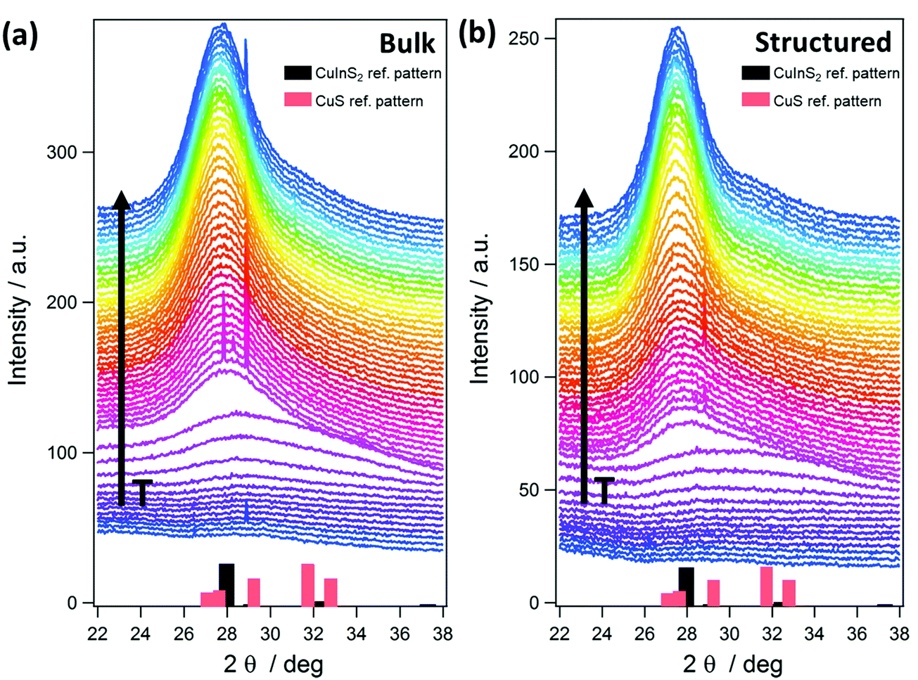 | ||
| Fig. 4 GIWAXS patterns of (a) bulk (non-structured) and (b) structured thin films measured between 22 and 38° 2θ during heating runs from 35 up to 400 °C with a heating rate of 10 °C min−1 and subsequent annealing of 15 min at 400 °C, displaying the formation of the (112) reflection of CuInS2 centred at 28.0° 2θ. Columns in the graph correspond to reference patterns of chalcopyrite CuInS2 structure (ICSD-42127) and covellite CuS (COD ID: 9000062). The increasing temperature (T) is indicated with a black arrow and the curves are shifted vertically for better visibility. | ||
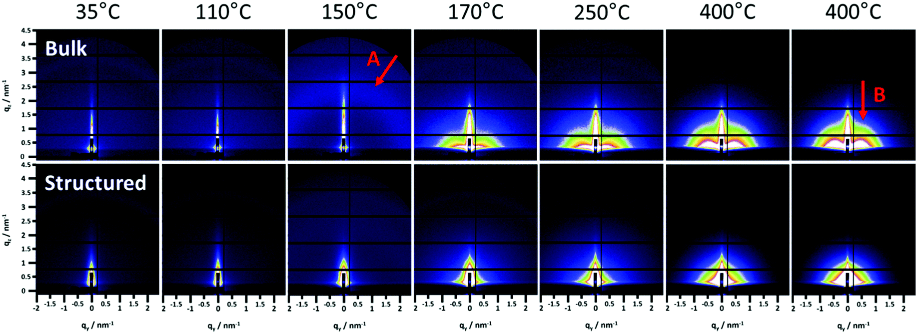 | ||
| Fig. 5 GISAXS patterns of the bulk (top) and structured (bottom) films at different temperatures starting from 35 up to 400 °C and 15 min annealing. Arrow A shows a semicircle like feature indicating a high order in the bulk film and arrow B points to the feature indicating the preferential near range order of the CuInS2 nanoparticles in the in-plane direction. | ||
The GIWAXS patterns (Fig. 4) and the corresponding surface plots (Fig. S5, ESI†) illustrate the formation of CuInS2 through the evolution of the (112) reflection of CuInS2, which is located at 28.0° 2θ. At a temperature of 35 °C, no diffraction peaks are visible, while a broad peak appears at a temperature of 130–135 °C. This broad peak is shifted to higher 2θ values (peak maximum at 29–30° 2θ) compared to the position of the (112) reflection of CuInS2. This indicates the formation of CuS seeds (reference pattern of covellite CuS, COD ID: 9000062), before the formation of the CuInS2 nanocrystals. At approx. 150–160 °C, the peak becomes significantly narrower and the position shifts to lower 2θ values, which corresponds to the typical peak position of chalcopyrite CuInS2 nanocrystals. This phenomenon is known for nanocrystal synthesis in solution,40 however, has not been observed so far in solventless conversion processes. Both the bulk and structured film display the same behaviour regarding the nanocrystal formation, but the formation of the CuS nanocrystals as well as the transformation to the CuInS2 nanocrystals occurs at slightly (5–10 °C) higher temperatures in the structured film, most presumably due to the presence of the PS template and the thereby decelerated heat transfer through the film. The sharp peaks visible in Fig. 4 and Fig. S5 (ESI†) at 2θ values of 27.8 and 28.9° at certain temperatures during the heating originate very likely from silicon crystals (impurity due to substrate cutting and handling) occasionally moving into the reflection conditions in these temperature ranges and are not stemming from the investigated CuInS2 thin films.
Further information can be extracted from the GIWAXS invariant and the evolution of the primary crystallite size determined using the Scherrer formula and the FWHM of the (112) reflection of CuInS2, as well as the GISAXS (Porod) invariant and correlation length41 shown in Fig. 6. The calculation of the invariant values as well as the correlation length is outlined in the ESI.†
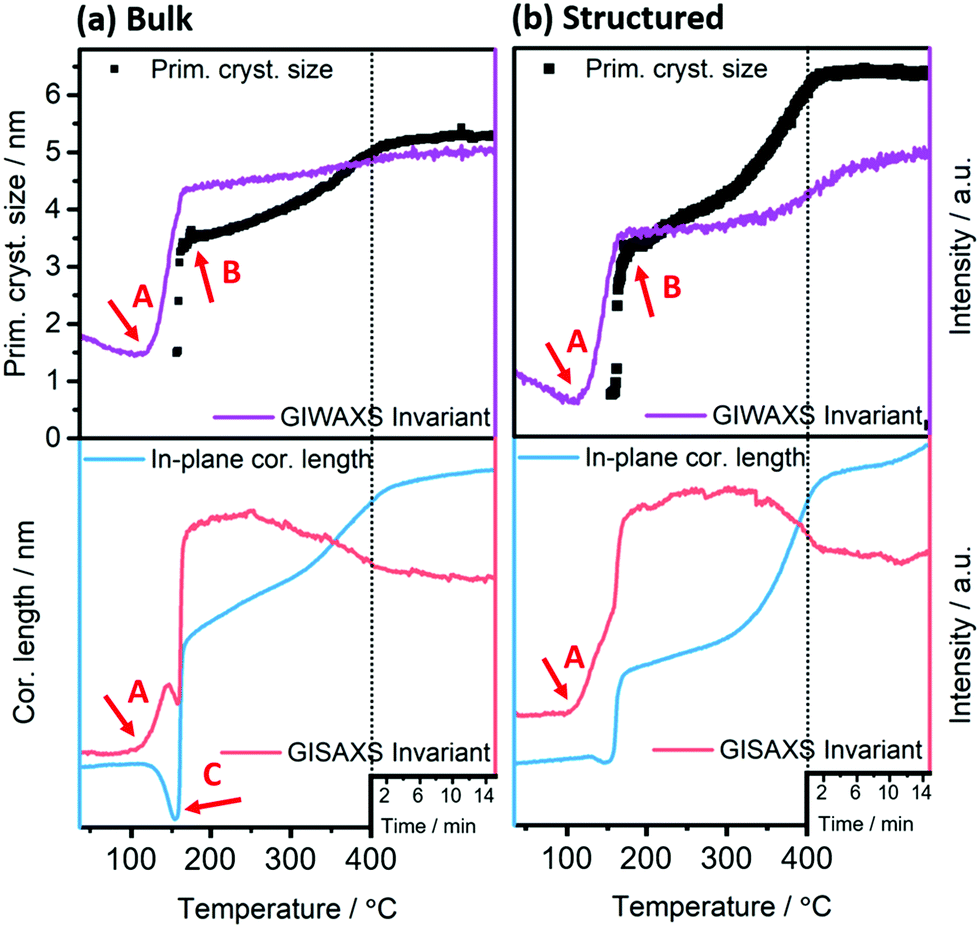 | ||
| Fig. 6 From top to bottom: GIWAXS invariant (purple) and the evolution of primary crystallite size (black) and GISAXS in-plane correlation length (blue) and invariant (red) during the heating run for (a) bulk as well as (b) structured films. Arrows A, B and C indicate the thermal conversion onset, offset and mesophase onset, respectively. The dashed lines denote the beginning of the annealing at constant temperature (400 °C) for 15 min. | ||
The onset of the conversion and the evaporation of organic decomposition products from the film leading to an increased electron density are indicated by an increase in the GIWAXS and GISAXS invariant at 114 °C (Fig. 6, arrow A) and the main conversion process is completed at 179 °C (arrow B). At that point, the primary crystallite size is 3.4 nm in the non-structured as well as the structured film. This fast conversion and nanocrystal growth are followed by a slower growth phase until approximately 300 °C. At this temperature the growth rate increases again and we assume that this phenomenon is based on an Ostwald ripening-type growth mechanism. However, it is apparent that in the case of the structured film, this step is much more pronounced (see Fig. 6a and b). This behaviour originates most likely from the combination of the Ostwald ripening-type mechanism and the decomposition of the polystyrene, which also starts at approximately 300 °C.42 We assume that polystyrene acts as a matrix for the CuInS2 at least in interfacial regions, which hinders the crystal growth, while upon its removal, the crystallite size remarkably increases. This assumption can be supported by the SEM images in Fig. S6 (ESI†) showing the structured film after the CuInS2 formation at 195 °C and before the polystyrene removal. The images illustrate a rather planar surface, where a hexagonal structure is distinguished underneath. Clear polystyrene sphere structures, however, are not visible after heating the film to 195 °C because the glass transition temperature of polystyrene has been exceeded.43 At 400 °C, primary crystallite sizes of 5.3 nm and 6.3 nm are obtained in the bulk and the structured films, respectively. The larger crystallite sizes in the structured film can be ascribed to the extended second growth phase (Ostwald ripening, growth after removal of polystyrene).
Moreover, the GISAXS images (shown for the bulk and structured films at different temperatures in Fig. 5) reveal additional information. In the bulk film, upon the xanthate conversion, an ordered mesophase is formed at approximately 150 °C by the decomposition products. This is indicated by a low intensity semicircle like feature (arrow A in Fig. 5), which is characteristic for an ordered phase, and also by the distinct minimum in the in-plane correlation length in Fig. 6(a) (bottom row, arrow C). While a minimum in the in-plane correlation length can also be recognized in the structured film, it is much less pronounced. Based on a previous study on a closely related materials system,44 we ascribe this mesophase to an ordered structure formed by the decomposition products of the metal xanthates during the first stage of the nanocrystal growth.
Additionally, the GISAXS image of the bulk film at 400 °C (arrow B in Fig. 5) indicates a preferential near range order of the CuInS2 nanocrystals in the in-plane direction. On the contrary, in the structured film, this preferential near range order is not observed.
In general, the concentration of the precursor solution, the spin coating speed and the drying process of the films are very important parameters in the formation of the CuInS2 honeycomb nanostructure. As an example, in Fig. S7 (ESI†) the FT-IR spectra and SEM images of films prepared with too high precursor concentration and too low spin coating speed are presented. The FT-IR spectrum before annealing shows both the PS-NS template and the xanthates, but the film was still not completely dry, as it is also indicated by the vibration peak at 3358 cm−1 corresponding to the OH-group of ethanol.45 This also significantly affects the final nanostructure, as the SEM images of these films only partly reveal the expected negative of the PS-NS template and also larger areas of compact CuInS2 films are formed on top of the template.
Based on these considerations, the reduction of the precursor concentration and the insertion of an additional drying step of the films at 90 °C for several minutes, between the infiltration and the decomposition step (heating ramp to 400 °C, 15 min holding time), led to well-defined honeycomb structures in case of the P300 and P600 templates. The SEM images in Fig. 7 illustrate the successful formation of honeycomb-structured CuInS2 films, which are in the following referred to as CIS-Px depending on the used nanosphere array template. In case of CIS-P300 and CIS-P600, homogeneous and ordered hexagonally-structured CuInS2 arrays were achieved. In the case of the CIS-P0 sample, no formation of a well-defined honeycomb structure could be obtained as still areas of CuInS2 films were formed above the honeycomb structure, leading to an inhomogeneous film surface (Fig. 7b). This is due to the tightly hexagonally packed PS nanospheres, which hinder the infiltration of sufficient amounts of the precursor solution.
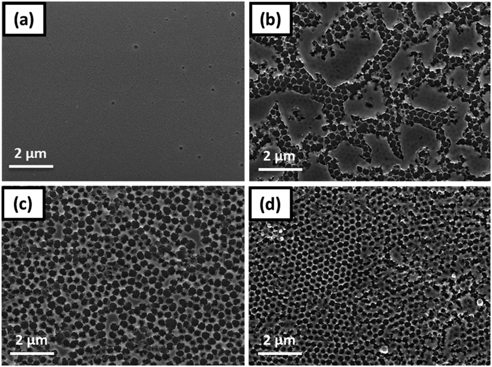 | ||
| Fig. 7 SEM images of (a) bulk-CIS (b) CIS-P0, (c) CIS-P300 and (d) CIS-P600 after annealing at 400 °C. | ||
As it can be clearly seen from the values in Table 1, the results of plasma etching have a pronounced impact on the dimensions of the nanostructures in the films. The wall thickness is higher for CIS-P600 (approx. 70 nm compared to 59 nm in the CIS-P300 sample), where a longer plasma etching process was applied leading to larger interstitial space between the spheres for the infiltration of the precursors and consequently also to smaller cell diameters. While in the CIS-P300 film cell diameters of 315 nm are observed, cell diameters of 234 nm are generated in the CIS-P600 sample.
| Precursor route | CIS-P300 | CIS-P600 | Bulk-CIS |
|---|---|---|---|
| Cell diameter (nm) | 315 ± 35 | 234 ± 21 | — |
| Wall thickness (nm) | 59 ± 21 | 70 ± 14 | — |
| Film thickness (nm) | 98 ± 5 | 101 ± 5 | 26 ± 1 |
Alternative methods to remove the template at lower temperatures did not lead to the expected result. For example, while thermal annealing of the sample at 280 °C in air resulted in the removal of the PS nanospheres, the remaining honeycomb structure was significantly oxidized. Moreover, soaking of the sample in chloroform after the conversion of the metal xanthates to CuInS2 at 195 °C led to an incomplete removal of the template. Details to these processes are summarized in the ESI.†
c. Formation of honeycomb-structured films via stabilized CuInS2 NCs – nanocrystal ink route
To realize the formation of honeycomb-structured CuInS2 films at low temperatures, we followed a second approach, which is based on the idea of forming the strctured thin films by employing already prepared capped CuInS2 NCs. Thus, a pre-synthesized and stabilized CuInS2 nanocrystal ink is used for infiltration of PS-NS templates. This provides an advantage during the formation of the CuInS2-scaffold in comparison to the in situ decomposition of the xanthates, in which a large amount of the decomposition products are leaving during the formation of the metal sulfide structures.The synthesis of the NCs was carried out by using copper and indium xanthates as precursors according to a previous study via a hot injection process and dioleamide (oleyl oleamide, N-((Z)-octadec-9-en-1-yl)oleamide) as capping ligand.32 The dioleamide is formed from the reaction of the oleylamine and oleic acid,46 while it stabilizes the NCs through the amide group. The dioleamide-capped CuInS2 NCs give stable dispersions in solvents, such as chloroform and toluene. However, the problem with these solvents is, as mentioned earlier, that they are not suitable for the infiltration of PS-NS templates. As the nature of the capping ligand plays an important role on the solubility of the nanocrystals, we modified the nanocrystals by a ligand exchange. Thiols are known as good capping ligands for the metal sulfide nanocrystals, specifically for quantum dots (QDs) due the crystal-bound ability, which means that the sulfur can actively participate in the surface of the crystal.47 Due to the strong binding, the thiol ligands cannot be easily replaced by other ligands, but they can easily replace other ligands, such as amine-based ligands.48 Thus, we exchanged the bulky dioleamide ligand by 1-thioglycerol (TG) via a ligand exchange procedure at 90 °C for 24 h. The thioglycerol-capped NCs form stable colloidal dispersions in solvents such as DMSO and DMF. Hence, we prepared NC inks in DMSO, which can be used for infiltration of the templates. Fig. 8 represents the process of the dioleamide-capped CuInS2 nanocrystal formation via hot injection and the subsequent ligand exchange with the thioglycerol.
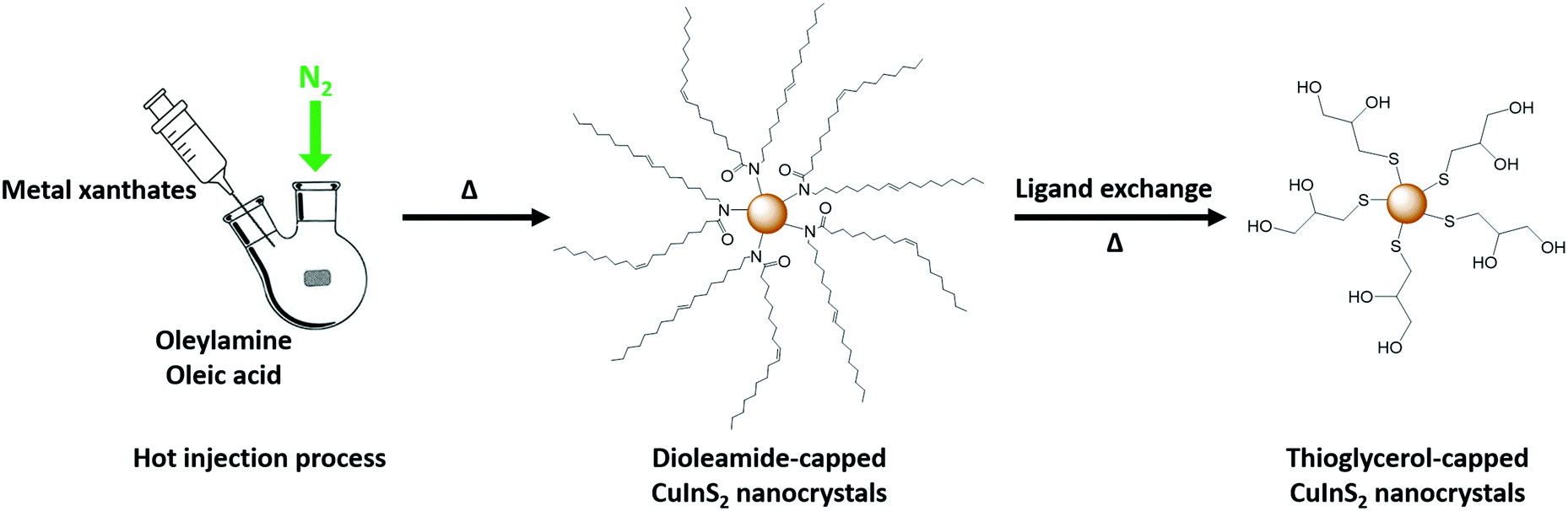 | ||
| Fig. 8 Representation of the dioleamide-capped NCs synthesis and ligand exchange with 1-thioglycerol. | ||
The FT-IR spectra of the dioleamide-capped NCs show vibrations at 1648 and 1563 cm−1, which correspond to CO group stretching and N–H group bending vibrations, as well as at 3307 and 3009 cm−1 that belong to the N–H group stretching vibration and to the amide group, respectively. Additionally, the XRD results reveal the typical diffraction peaks of the CuInS2 chalcopyrite crystal structure (ICSD-42127), while from the peak broadening and the Scherrer equation, a nanocrystal size of approximately 3.6 nm was determined, which also fits with previous studies.14,32
In order to investigate the success of the ligand exchange, an FT-IR measurement was performed. The FT-IR spectra in Fig. 9(a) illustrate the results before and after the exchange, as well as the free 1-thioglycerol. The spectrum after the exchange fits quite well with the free 1-thioglycerol, indicating the successful replacement of the dioleamide ligand. Specifically, the broad peak at 3331 cm−1 corresponds to the stretching vibration of OH-group, while the absence of the peak at 2554 cm−1, which belongs to the stretching vibration of the SH-group, reveals that there is no unbound thioglycerol present. Simultaneously, the XRD pattern after the ligand exchange resembles the one before the exchange (Fig. S11, ESI†), while the crystal size is determined to be also approximately 3.6 nm, meaning that the process does not influence the size. Lastly, the UV-vis absorption spectra of the NCs before and after ligand exchange in Fig. S12 (ESI†), illustrate the typical absorption curve of the CuInS2 nanocrystals with an absorption onset at approximately 850 nm, corresponding to an optical band gap of 1.45 eV.
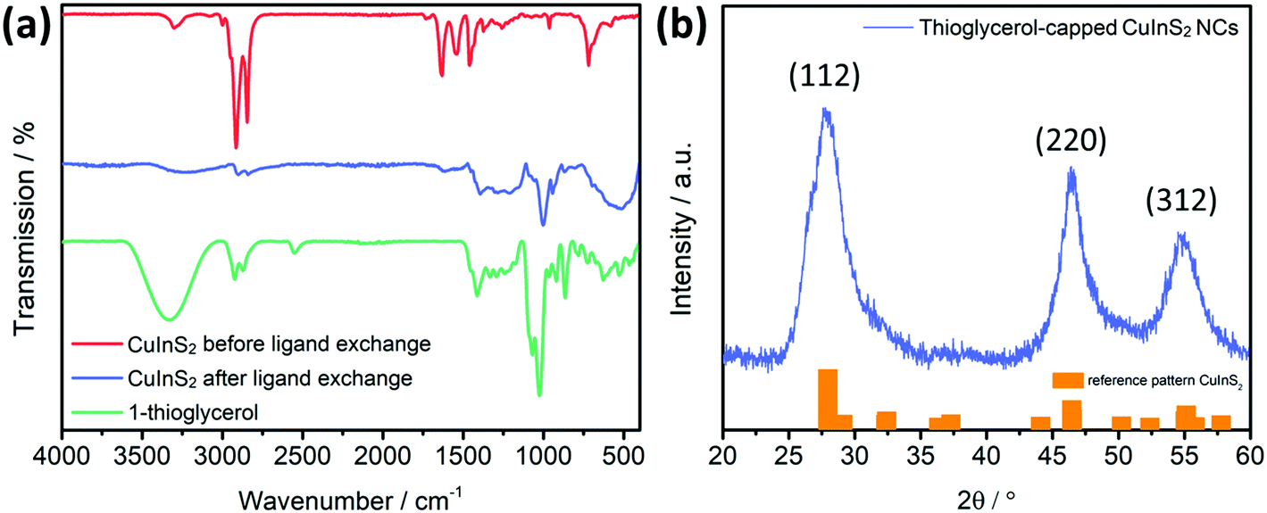 | ||
| Fig. 9 (a) FT-IR spectra before (red spectrum) and after the ligand exchange (blue spectrum) and free 1-thioglycerol (green spectrum). The spectra are shifted vertically for better visibility. (b) X-Ray diffraction pattern of the CuInS2 nanocrystals after ligand exchange, with reference patterns for chalcopyrite CuInS2 (ICSD-42127). | ||
In the next step, the PS-NS template P600 was infiltrated with the CuInS2 nanocrystal ink in DMSO. Specifically, the CuInS2 ink with a concentration 100 mg mL−1 was infiltrated via a few seconds of soaking followed by spin coating with 1000 rpm rotation speed. After a drying process of the samples at 90 °C, the samples were immersed in toluene for the template removal. The FT-IR spectra in Fig. 10(a) display the characteristics before and after immersion. In both spectra, only the vibration bands of the polystyrene are identified. A potential explanation for the absence of vibrations, which correspond to the thioglycerol-capped CuInS2, could be the low intensity signals of the initial material, as it can be seen in Fig. 9(a) in comparison to the signals of the free 1-thioglycerol. This, in combination with the usage of a low concentration of the ink, leads to the lack of vibrational bands corresponding to the stabilized NCs. Moreover, after the immersion of the samples in toluene, it is noticed that polystyrene remains on the film. However, the intensity of the signals is significantly reduced, indicating that the template is widely removed. The remaining bands in the IR spectrum can be attributed to trapped polystyrene among the NCs. The SEM image in Fig. 10(b) shows that the procedure was successful, resulting in well-defined hexagonal-structured thin films. Information regarding the pore diameter, wall and film thickness are summarized in Table 2. The cell (∼264 nm) and wall sizes (∼78 nm) fit well with the values obtained for the CIS-P600 with the precursor route, as in both cases the P600 PS-NS template was used. Moreover, the GIXRD pattern of the structured film (Fig. S14, ESI†) reveals a broad peak around 28° 2θ stemming from the 112 reflection of the chalcopyrite crystal structure of the CuInS2 nanocrystals. Similar to the structured films prepared via the precursor route, these samples also display a structural colour. After the infiltration of the NCs, the films do not appear coloured, because there is no defined structure. On the contrary, when the template is removed, the inverse structure of the CuInS2 NCs remains and hence, the films appear blue (see Fig. S13, ESI†).
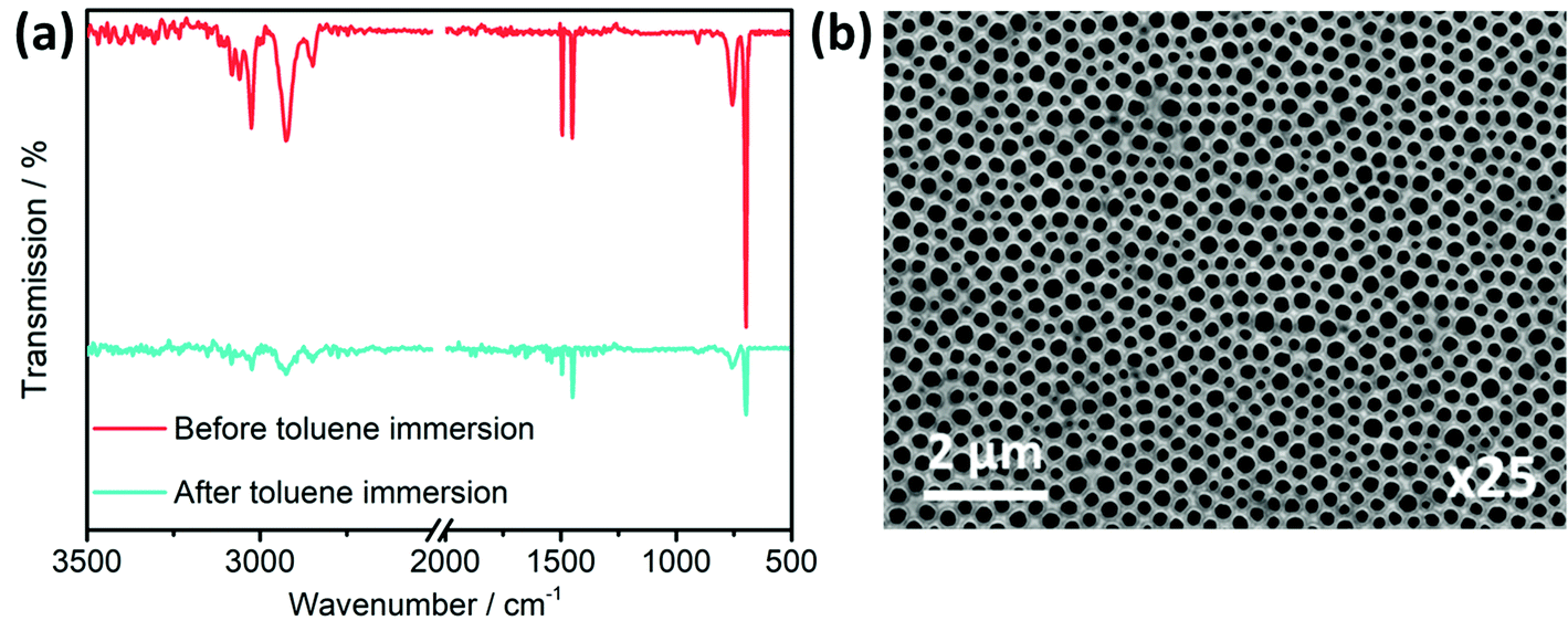 | ||
| Fig. 10 (a) FT-IR spectra of thin films before and after immersion of the infiltrated thin films in toluene. The spectra are shifted vertically for better visibility. (b) SEM images of the honeycomb-structured CuInS2 thin films after template removal. | ||
| Nanocrystal ink route | |
|---|---|
| Cell diameter (nm) | 264 ± 30 |
| Wall thickness (nm) | 78 ± 17 |
| Film thickness (nm) | 75 ± 2 |
Conclusion
In summary, we developed two novel, cost-efficient and scalable routes towards the formation of honeycomb-structured CuInS2 thin films via nanosphere colloidal lithography. A mixture of copper and indium xanthates, as metal sulfide precursors was used in the first route for the in situ formation of CuInS2. For the second route pre-synthesized thioglycerol-capped CuInS2 NCs were employed. The PS-NS template layer was fabricated via an air/liquid interface method and subsequently modified with O2 plasma etching. The plasma etching was essential for increasing the interstitial space between the spheres and hence, facilitating the infiltration process.In the first route, the infiltration of the template with the metal xanthate solution was followed by the in situ formation of the nanocrystalline CuInS2 through the thermal decomposition of the xanthate mixture at 195 °C. The conversion to the metal sulfide starts already at 114 °C, a temperature at which the PS-NS template is stable. By further heating to 400 °C, the PS template is removed, resulting in a well-defined honeycomb-structured CuInS2 film.
For the second approach, dioleamide-capped CuInS2 NCs were first synthesized via a hot injection synthesis followed by a ligand exchange leading to thioglycerol-capped CuInS2 NCs. The thioglycerol ligands enabled the infiltration of the PS-NS templates with a DMSO based nanocrystal ink, which was not possible with the dioleamide-capped CuInS2 NCs, as they are only soluble in solvents, which also readily dissolve polystyrene. In this route, an annealing step after the infiltration could be omitted and thus a good solubility of the template is retained. After dissolving the template at room temperature in toluene, the honeycomb structured metal sulfide film is obtained.
Experimental section
All chemicals and solvents were used as purchased without any additional purification: dichloromethane (≥99.8%, Fisher Chemical), dichlorobenzene (CHROMASOLV®, 99%, Sigma-Aldrich), toluene (≥99%), methanol (VWR), ethanol (≥99.8%, Sigma-Aldrich), dimethyl sulfoxide (DMSO, ≤0.02% water, Sigma-Aldrich), hexane (≥99%,), polystyrene nanospheres (Latex beads, LB3, 0.3 μm mean particle size), sodium dodecyl sulfate (SDS, ≥95%, ROTH), ethanolamine (≥99%, Sigma-Aldrich), oleylamine (approximate C18-content 80–90%, ACROS ORGANICS), oleic acid (technical grade 90%, Sigma-Aldrich) and 1-thioglycerol (≥97%, Sigma-Aldrich). Copper and indium xanthates (copper and indium O-2,2-dimethylpentan-3-yl dithiocarbonate, respectively) were synthesized according to a previous work.33a. Preparation of the polystyrene nanosphere templates
The polystyrene nanosphere templates (PS-NS) with sphere sizes of approximately 300 nm were prepared by a self-assembly approach at the air/water interface, according to previous work.49 The detailed process is described below. A 1:1 volume ratio of an aqueous PS colloidal suspension with ethanol was prepared and was dispersed for 10 minutes in a sonication bath. Subsequently, the suspension was dropped (∼100 μL) onto a glass slide (1.5 × 1.5 cm), which was placed in the centre of a glass Petri dish. Deionized water was slowly added until a convex shape was formed around the glass slide, where the PS suspension was rapidly spread on the water/air interface, leading to the two-dimensional layer assembly. In order to closely-pack the polystyrene layer, a few drops of 2 wt% SDS aqueous solution were added. A large area of a blueish PS layer (structural color) at the air/liquid interface was observed, which indicated the formation of the closely-packed layer. To transfer the PS closely-packed layer on the substrate (glass and Si substrates), the latter was inserted beneath the floating layer and carefully lifted off from the water. Finally, the wet layers were dried at room temperature for several hours. After drying, PS-NS layers were transferred into an O2 plasma reactor chamber (FEMTO, Diener Electronic) for size modification. The O2 plasma etching was performed for 0, 300 and 600 s under an excitation frequency of 40 kHz, a power of 100 W and a gas flow of 20 sccm.
b. Preparation of honeycomb-structured films via in situ CuInS2 formation
The honeycomb-structured CuInS2 films were fabricated by spin coating of the CuInS2 precursor solution. The solution was prepared by dissolving copper O-2,2-dimethylpentan-3-yl dithiocarbonate (16.1 mg mL−1, 1 equiv.) and indium O-2,2-dimethylpentan-3-yl dithiocarbonate (73.9 mg mL−1, 1.7 equiv.) in a solvent mixture of 1000:500:50 μL ethanol:dichloromethane:ethanolamine. The solution is stable for approximately 4 h, thus the infiltration should be completed directly after its preparation. The infiltration of the PS-NS templates was performed by spin-coating of the precursor solution (5000 rpm rotation speed, 60 s). The infiltrated samples were then dried on a hot plate at 90 °C under ambient atmosphere for 10 min. Finally, the samples were annealed at 400 °C (heating rate 10 °C min−1) for 15 min under inert atmosphere, in order to form the CuInS2, decompose the PS-NS and result the honeycomb-CuInS2 films. Additionally, bulk CuInS2 films were prepared following the same procedure, but a lower amount of solvent in a slightly adjusted mixture was used (700:350:50 μL ethanol:dichloromethane:ethanolamine) for dissolving the copper and indium xanthates (16.1 mg and 73.9 mg, respectively) to obtain higher film thicknesses.
c. Nanocrystal synthesis
5 mL oleylamine and 5 mL oleic acid were placed in a three-neck round bottom flask with a stirrer and heated to 200 °C under inert conditions. A total amount of 0.5 mmol of the copper and indium O-2,2-dimethylpentan-3-yl-dithiocarbonate (Cu(Hep) and In(Hep)3, respectively) in a ratio of 1:1.7 were dissolved in 3 mL dichlorobenzene and injected in the hot reaction mixture and kept for 30 min. Subsequently, the mixture was left to cool down naturally to room temperature. By addition of methanol, the nanocrystals were precipitated and collected by centrifugation. The solid material was redispersed in toluene, precipitated with methanol and collected again by centrifugation. The clean solid was finally dispersed in toluene.
d. Ligand exchange
The CuInS2 nanocrystals capped with the dioleamide (product of oleylamine and oleic acid at high temperatures) ligand were put in 4 mL of 1-thioglycerol and heated to 90 °C under nitrogen atmosphere. After 24 h stirring, the solution was cooled down to room temperature and purified by a dichloromethane/hexane mixture. The precipitated material was collected by centrifugation. Subsequently, the solid was redispersed in DMSO, precipitated and centrifuged. The final material was dispersed in DMSO.e. Preparation of honeycomb-structured films via stabilized CuInS2 NCs
The honeycomb-structured thin films were formed by using the thioglycerol-capped CuInS2 nanocrystals in DMSO. The dispersion with a concentration of 100 mg mL−1 was infiltrated in the PS-NS templates by spin coating at 1000 rpm for 60 s. The infiltrated samples were then dried on a hot plate at 90 °C under ambient atmosphere for 10 min. Finally, the template was removed via immersing the samples in toluene for 5 min in order to produce the structured thin films.f. Characterization
FT-IR spectra were measured on a Bruker Alpha FT-IR spectrometer in transmission mode (layers on silicon wafers). All spectra were recorded in a range between 3600 and 500 cm−1 with 24 scans and a blank silicon wafer as background. UV-Vis absorption spectra were recorded on a Shimadzu spectrophotometer UV-1800 (300 to 1000 nm).The grazing incidence X-ray diffraction measurements were performed on a Rigaku SmartLab II X-ray diffractometer, which features the PhotonMax high-flux 9 kW rotating anode X-ray source, with a D/teX Ultra 250 detector. The measurements were performed in an incidence angle of 0.8°. The powder X-ray diffraction (XRD) measurements were taken on a RIGAKU Miniflex 600 with D/Tex Ultra detector using CuKα radiation (λ = 1.5418 Å). The measurements were performed on a zero-background sample holder. The diffraction patterns were evaluated with the SmartLabStudioIIx64v4.2.890 software.
Scanning electron microscopic images were acquired on a TESCAN MIRA3 Field Emission Scanning Electron Microscope (FESEM) using an In-Beam secondary electron (SE) detector. The microscope was operated at 5 kV, with a working distance of about 4 mm and an electron beam spot size of 4 nm. Samples for FESEM characterisations were coated with a 5 nm thin chromium layer by thermal evaporation. Energy Dispersive Spectroscopy (EDX) investigations were carried out with a Super Octane detector with a 60 mm2 active area (EDAX AMETEK, Mahwah, NJ, USA), using a working distance of 10 mm and an acceleration voltage of 15 kV.
Simultaneous GISAXS and GIWAXS measurements were performed at the Austrian SAXS Beamline 5.2 L of the electron storage ring ELETTRA (Italy).50 The setup had been adjusted to a q-range (q = 4π/λsin(2θ/2)) between 0.1 and 2.4 nm−1 in in-plane and between 0.6 and 4.3 nm−1 in out-of-plane direction (GISAXS) as well as to resolve the angular range (2θ) between 20.3 and 40.0° in the GIWAXS characterizations. The measurements were performed at a photon energy of 8 keV. The samples were mounted on an Anton Paar DHS 1100 heating cell equipped with a specially designed dome having Kapton windows to provide high X-ray transmissivity and low background. The GIWAXS signal was monitored using a Dectris Pilatus 100k detector and the GISAXS signal with a Dectris Pilatus3 1M detector. The angular calibration of the detectors was carried out using p-bromo benzoic acid and silver behenate powder (d-spacing of 58.38 Å), respectively. The sample chamber was purged with nitrogen during the whole experiment. The temperature range used was from 35 up to 400 °C with a heating rate of 10 °C min−1. A temperature resolution of 1 °C could be obtained by having one frame every 6 seconds (5 seconds exposure). All measurements have been performed with a grazing angle of 0.23°. The off specular out-of-plane integration was done in a q-range between −0.06 to 0.03 nm−1 and the in-plane integration between 0.21–0.48 nm−1 (Fig. S3, ESI†) with the data evaluation software SAXS DOG.51
Conflicts of interest
There are no conflicts to declare.Acknowledgements
The authors gratefully acknowledge Graz University of Technology for financial support through the Lead Project Porous Materials at Work (LP-03). Moreover, the authors acknowledge the CERIC-ERIC consortium for the access to experimental facilities (Austrian SAXS beamline at Elettra Sincrotrone Trieste) and financial support.References
- (a) P. Innocenzi and L. Malfatti, Chem. Soc. Rev., 2013, 42, 4198–4216 RSC; (b) P. Kumar, K.-H. Kim, K. Vellingiri, P. Samaddar, P. Kumar, A. Deep and N. Kumar, Biosens. Bioelectron., 2018, 104, 120–137 CrossRef CAS PubMed; (c) L. Zhang, Z.-J. Zhao and J. Gong, Angew. Chem., Int. Ed., 2017, 56, 11326–11353 CrossRef CAS PubMed.
- Z. Wang, D. Cao, R. Xu, S. Qu, Z. Wang and Y. Lei, Nano Energy, 2016, 19, 328–362 CrossRef CAS.
- Y. Shi, Y. Wan and D. Zhao, Chem. Soc. Rev., 2011, 40, 3854–3878 RSC.
- (a) S. Shen and Q. Wang, Chem. Mater., 2013, 25, 1166–1178 CrossRef CAS; (b) C.-H. Lai, M.-Y. Lu and L.-J. Chen, J. Mater. Chem., 2012, 22, 19–30 RSC; (c) S. M. Gupta and M. Tripathi, High Energy Chem., 2012, 46, 1–9 CrossRef CAS; (d) G. Wang, C. Li and H. Shan, ACS Catal., 2014, 4, 1139–1143 CrossRef CAS.
- S. Chandrasekaran, L. Yao, L. Deng, C. Bowen, Y. Zhang, S. Chen, Z. Lin, F. Peng and P. Zhang, Chem. Soc. Rev., 2019, 48, 4178–4280 RSC.
- M.-H. Sun, S.-Z. Huang, L.-H. Chen, Y. Li, X.-Y. Yang, Z.-Y. Yuan and B.-L. Su, Chem. Soc. Rev., 2016, 45, 3479–3563 RSC.
- A. Fischereder, M. L. Martinez-Ricci, A. Wolosiuk, W. Haas, F. Hofer, G. Trimmel and G. J. A. A. Soler-Illia, Chem. Mater., 2012, 24, 1837–1845 CrossRef CAS.
- Y. Türker and Ö. Dag, J. Mater. Chem., 2008, 18, 3467–3473 RSC.
- H. Zhou, H. Xiong, R. Zhang, L. Zhang, L. Zhang, L. Li, W. Zhang, Z. Zhu and Z.-A. Qiao, Small, 2021, 17, 2100428 CrossRef CAS PubMed.
- Y. Guo, J. Tang, J. Henzie, B. Jiang, W. Xia, T. Chen, Y. Bando, Y.-M. Kang, M. S. A. Hossain, Y. Sugahara and Y. Yamauchi, ACS Nano, 2020, 14, 4141–4152 CrossRef CAS PubMed.
- B. T. Yonemoto, G. S. Hutchings and F. Jiao, J. Am. Chem. Soc., 2014, 136, 8895–8898 CrossRef CAS PubMed.
- T. Rath, C. Padeste, M. Vockenhuber, C. Fradler, M. Edler, A. Reichmann, I. Letofsky-Papst, F. Hofer, Y. Ekinci and T. Griesser, J. Mater. Chem. A, 2013, 1, 11135–11140 RSC.
- (a) C. Buchmaier, M. Glänzer, A. Torvisco, P. Poelt, K. Wewerka, B. Kunert, K. Gatterer, G. Trimmel and T. Rath, J. Mater. Sci., 2017, 52, 10898–10914 CrossRef CAS; (b) S. A. Alderhami, D. Collison, D. J. Lewis, P. D. McNaughter, P. O'Brien, B. F. Spencer, I. Vitorica-Yrezabal and G. Whitehead, Dalton Trans., 2019, 48, 15605–15612 RSC.
- C. Buchmaier, T. Rath, F. Pirolt, A.-C. Knall, P. Kaschnitz, O. Glatter, K. Wewerka, F. Hofer, B. Kunert, K. Krenn and G. Trimmel, RSC Adv., 2016, 6, 106120–106129 RSC.
- (a) B. Radha, S. Kiruthika and G. U. Kulkarni, J. Am. Chem. Soc., 2011, 133, 12706–12713 CrossRef CAS PubMed; (b) L. Persano, A. Camposeo, F. Di Benedetto, R. Stabile, A. M. Laera, E. Piscopiello, L. Tapfer and D. Pisignano, Adv. Mater., 2012, 24, 5320–5326 CrossRef CAS PubMed; (c) M. S. M. Saifullah, M. Asbahi, M. Binti-Kamran Kiyani, S. S. Liow, S. Bin Dolmanan, A. M. Yong, E. A. H. Ong, A. Ibn Saifullah, H. R. Tan, N. Dwivedi, T. Dutta, R. Ganesan, S. Valiyaveettil, K. S. L. Chong and S. Tripathy, ACS Appl. Mater. Interfaces, 2020, 12, 16772–16781 CrossRef CAS PubMed; (d) J. Recatala-Gomez, H. K. Ng, P. Kumar, A. Suwardi, M. Zheng, M. Asbahi, S. Tripathy, I. Nandhakumar, M. S. M. Saifullah and K. Hippalgaonkar, ACS Appl. Mater. Interfaces, 2020, 12, 33647–33655 CrossRef CAS PubMed; (e) M. S. M. Saifullah, M. Asbahi, M. Binti-Kamran Kiyani, S. Tripathy, E. A. H. Ong, A. Ibn Saifullah, H. R. Tan, T. Dutta, R. Ganesan, S. Valiyaveettil and K. S. L. Chong, ACS Nano, 2017, 11, 9920–9929 CrossRef CAS PubMed.
- Y. Lu, J. Jia and G. Yi, CrystEngComm, 2012, 14, 3433–3440 RSC.
- Y.-H. Hung, A.-Y. Lu, Y.-H. Chang, J.-K. Huang, J.-K. Chang, L.-J. Li and C.-Y. Su, ACS Appl. Mater. Interfaces, 2016, 8, 20993–21001 CrossRef CAS PubMed.
- R. van Dommelen, P. Fanzio and L. Sasso, Adv. Colloid Interface Sci., 2018, 251, 97–114 CrossRef CAS PubMed.
- H. W. Deckman and J. H. Dunsmuir, Appl. Phys. Lett., 1982, 41, 377–379 CrossRef CAS.
- (a) P. Labouchere, A. K. Chandiran, T. Moehl, H. Harms, S. Chavhan, R. Tena-Zaera, M. K. Nazeeruddin, M. Graetzel and N. Tetreault, Adv. Energy Mater., 2014, 4, 1400217 CrossRef; (b) S.-E. Cheon, H.-S. Lee, J. Choi, A. R. Jeong, T. S. Lee, D. S. Jeong, K.-S. Lee, W.-S. Lee, W. M. Kim, H. Lee and I. Kim, Sci. Rep., 2017, 7, 7336 CrossRef PubMed; (c) Y. G. Seo, K. Woo, J. Kim, H. Lee and W. Lee, Adv. Funct. Mater., 2011, 21, 3094–3103 CrossRef CAS; (d) G. von Freymann, V. Kitaev, B. V. Lotsch and G. A. Ozin, Chem. Soc. Rev., 2013, 42, 2528–2554 RSC.
- X. Ye and L. Qi, Nano Today, 2011, 6, 608–631 CrossRef CAS.
- (a) X. Chen, S. Yang, Y. C. Zheng, Y. Chen, Y. Hou, X. H. Yang and H. G. Yang, Adv. Sci., 2015, 2, 1500105 CrossRef PubMed; (b) L. Zhang, M. T. Hörantner, W. Zhang, Q. Yan and H. J. Snaith, Sol. Energy Mater. Sol. Cells, 2017, 160, 193–202 CrossRef CAS.
- M. T. Hörantner, W. Zhang, M. Saliba, K. Wojciechowski and H. J. Snaith, Energy Environ. Sci., 2015, 8, 2041–2047 RSC.
- C. Geng, F. Li, Y. Fan, L. Zhang, S. Shi, Z.-H. Zhang, Y. Zhang, S. Xu and W. Bi, Cryst. Growth Des., 2018, 18, 5770–5779 CrossRef CAS.
- S. Amrehn, D. Berghoff, A. Nikitin, M. Reichelt, X. Wu, T. Meier and T. Wagner, Photonics Nanostructures – Fundam. Appl., 2016, 19, 55–63 CrossRef.
- L. Galle, S. Ehrling, S. Lochmann, S. Kaskel, L. Bischoff and J. Grothe, ChemNanoMat, 2020, 6, 560–566 CrossRef CAS.
- (a) S. Schünemann, K. Chen, S. Brittman, E. Garnett and H. Tüysüz, ACS Appl. Mater. Interfaces, 2016, 8, 25489–25495 CrossRef PubMed; (b) F. Zhang, J. Song, M. Chen, J. Liu, Y. Hao, Y. Wang, J. Qu and P. Zeng, Phys. Chem. Chem. Phys., 2016, 18, 32903–32909 RSC.
- Z. Yi, G. Niu, J. Luo, X. Kang, W. Yao, W. Zhang, Y. Yi, Y. Yi, X. Ye, T. Duan and Y. Tang, Sci. Rep., 2016, 6, 32314 CrossRef CAS PubMed.
- T. Fan, P. Sun, J. Zhao, Z. Cui and G. Cui, J. Electrochem. Soc., 2019, 166, D37–D43 CrossRef CAS.
- (a) R. Klenk, J. Klaer, R. Scheer, M. Lux-Steiner, I. Luck, N. Meyer and U. Rühle, Thin Solid Films, 2005, 480-481, 509–514 CrossRef CAS; (b) W. Chen, J. Qi, C. Dong, J. Chen, Z. Shen, Y. He, S. Yang, T. Chen, C. Chen, Y. Li, M.-D. Li and M. Wang, ACS Appl. Energy Mater., 2019, 2, 5231–5242 CrossRef CAS.
- A. Fischereder, T. Rath, W. Haas, H. Amenitsch, D. Schenk, A. Zankel, R. Saf, F. Hofer and G. Trimmel, ACS Appl. Mater. Interfaces, 2012, 4, 382–390 CrossRef CAS PubMed.
- V. Perner, T. Rath, F. Pirolt, O. Glatter, K. Wewerka, I. Letofsky-Papst, P. Zach, M. Hobisch, B. Kunert and G. Trimmel, New J. Chem., 2019, 43, 356–363 RSC.
- T. Rath, M. Edler, W. Haas, A. Fischereder, S. Moscher, A. Schenk, R. Trattnig, M. Sezen, G. Mauthner, A. Pein, D. Meischler, K. Bartl, R. Saf, N. Bansal, S. A. Haque, F. Hofer, E. J. W. List and G. Trimmel, Adv. Energy Mater., 2011, 1, 1046–1050 CrossRef CAS.
- (a) H. Zhao, M. Zhou, L. Wen and Y. Lei, Nano Energy, 2015, 13, 790–813 CrossRef CAS; (b) J. Weickert, R. B. Dunbar, H. C. Hesse, W. Wiedemann and L. Schmidt-Mende, Adv. Mater., 2011, 23, 1810–1828 CrossRef CAS PubMed.
- (a) J. Yu and C.-W. Kan, Fibers, 2018, 6, 70 CrossRef CAS; (b) P. Liu, L. Bai, J. Yang, H. Gu, Q. Zhong, Z. Xie and Z. Gu, Nanoscale Adv., 2019, 1, 1672–1685 RSC.
- (a) Y.-Y. Lin, Y.-J. Chen, F.-G. Tseng and D.-J. Yao, IEEE Nanotechnol. Mag., 2014, 8, 20–28 Search PubMed; (b) J. A. Yabagi, M. I. Kimpa, M. N. Muhammad, N. Nayan, Z. Embong and M. Arif Agam, J. Sci. Technol., 2017, 9, 145–153 Search PubMed; (c) A. Plettl, F. Enderle, M. Saitner, A. Manzke, C. Pfahler, S. Wiedemann and P. Ziemann, Adv. Funct. Mater., 2009, 19, 3279–3284 CrossRef CAS.
- S. Dunst, T. Rath, A. Radivo, E. Sovernigo, M. Tormen, H. Amenitsch, B. Marmiroli, B. Sartori, A. Reichmann, A.-C. Knall and G. Trimmel, ACS Appl. Mater. Interfaces, 2014, 6, 7633–7642 CrossRef CAS PubMed.
- E. Vakalopoulou, C. Buchmaier, A. Pein, R. Saf, R. C. Fischer, A. Torvisco, F. Warchomicka, T. Rath and G. Trimmel, Dalton Trans., 2020, 49, 14564–14575 RSC.
- J. Fang, Y. Xuan and Q. Li, Sci. China: Technol. Sci., 2010, 53, 3088–3093 CrossRef CAS.
- T. Kuzuya, Y. Hamanaka, K. Itoh, T. Kino, K. Sumiyama, Y. Fukunaka and S. Hirai, J. Colloid Interface Sci., 2012, 388, 137–143 CrossRef CAS PubMed.
- (a) O. Glatter and O. Kratky, Small Angle X-Ray Scattering. Chapter 2 General Theory by Porod, Academic Press INC LTD., London, 1982 Search PubMed; (b) H. M. A. Ehmann, O. Werzer, S. Pachmajer, T. Mohan, H. Amenitsch, R. Resel, A. Kornherr, K. Stana-Kleinschek, E. Kontturi and S. Spirk, ACS Macro Lett., 2015, 4, 713–716 CrossRef CAS.
- J. D. Peterson, S. Vyazovkin and C. A. Wight, Macromol. Chem. Phys., 2001, 202, 775–784 CrossRef CAS.
- J. E. Mark, The polymer data handbook, Oxford University Press, New York, Oxford, 2nd edn, 2009 Search PubMed.
- E. Vakalopoulou, T. Rath, M. Kräuter, A. Torvisco, R. C. Fischer, B. Kunert, R. Resel, H. Schröttner, A. M. Coclite, H. Amenitsch and G. Trimmel, ACS Appl. Nano Mater., 2022, 5, 1508–1520 CrossRef CAS.
- A. Aldiyarov, M. Aryutkina, A. Drobyshev, M. Kaikanov and V. Kurnosov, Low Temp. Phys., 2009, 35, 251–255 CrossRef CAS.
- D. G. Calatayud, T. Jardiel, M. Rodríguez, M. Peiteado, D. Fernández-Hevia and A. C. Caballero, Ceram. Int., 2013, 39, 1195–1202 CrossRef CAS.
- M. J. Turo and J. E. Macdonald, ACS Nano, 2014, 8, 10205–10213 CrossRef CAS PubMed.
- J. Choi, W. Choi and D. Y. Jeon, ACS Appl. Nano Mater., 2019, 2, 5504–5511 CrossRef CAS.
- J. Yu, Q. Yan and D. Shen, ACS Appl. Mater. Interfaces, 2010, 2, 1922–1926 CrossRef CAS PubMed.
- H. Amenitsch, M. Rappolt, M. Kriechbaum, H. Mio, P. Laggner and S. Bernstorff, J. Synchrotron Radiat., 1998, 5, 506–508 CrossRef CAS PubMed.
- M. Burian, C. Meisenbichler, D. Naumenko and H. Amenitsch, SAXSDOG: open software for real-time azimuthal integration of 2D scattering images. https://arxiv.org/abs/2007.02022v1.
Footnote |
| † Electronic supplementary information (ESI) available: Additional SEM images, SEM-EDX, GIWAXS and GISAXS data, FT-IR and UV-vis spectra. See DOI: 10.1039/d2ma00004k |
| This journal is © The Royal Society of Chemistry 2022 |