
 Open Access Article
 This Open Access Article is licensed under a Creative Commons Attribution-Non Commercial 3.0 Unported Licence
Combinatorial ALD for the growth of ZnO/TiO2 nanolaminates and mixed ZnO/TiO2 nanostructured films
Shóna
Doyle
 *a,
Louise
Ryan
a,
Melissa M.
McCarthy
ab,
Mircea
Modreanu
a,
Michael
Schmidt
a,
Fathima
Laffir
c,
Ian M.
Povey
a and
Martyn E.
Pemble
ad
*a,
Louise
Ryan
a,
Melissa M.
McCarthy
ab,
Mircea
Modreanu
a,
Michael
Schmidt
a,
Fathima
Laffir
c,
Ian M.
Povey
a and
Martyn E.
Pemble
ad
aTyndall National Institute, University College Cork, Cork, Ireland. E-mail: shona.doyle@tyndall.ie
bDepartment of Physics, University of Oxford, Clarendon Laboratory, Parks Road, Oxford, UK
cDepartment of Chemical Sciences and Bernal Institute, University of Limerick, Limerick, Ireland
dSchool of Chemistry, University College Cork, Cork, Ireland
First published on 24th February 2022
Abstract
In this study, combinatorial atomic layer deposition (C-ALD) has been used to deposit layered ZnO and TiO2 nanolaminates on both oxide-covered Si(100) wafers and glass substrates to assess the influence of substrate and each layer on the structure of the resulting nanolaminates and their photoactivity towards dye degradation. In addition, for comparison to these layered structures, C-ALD has been used to directly create oxide films consisting of an approximately equal mixture of Zn2+ and Ti4+ ions using the concept of under-dosing in order to deposit sub-monolayer quantities of each oxide per complete C-ALD cycle. A nucleation delay was observed for ZnO deposited directly on the substrate and the subsequent TiO2 layer, the latter to a lesser extent. The reason for the difference in nucleation delay is due to the dissimilar surface groups. For the deliberately layered structures, it was found that ZnO appeared to possess a templating influence on the TiO2 layer grown subsequently on both substrate types. XRD analysis showed strong preferential orientation for (002) which indicates the polycrystalline manner of the ZnO film. XRD results also suggested that layer growth was substrate-dependent as crystalline TiO2 was only identified on glass substrates. The nanolaminate structures were found to be stable in that the layer structure remained intact after annealing at 400 °C for 1 hour in contrast to the comparison to the mixed ZnO![[thin space (1/6-em)]](https://www.rsc.org/images/entities/char_2009.gif) :TiO2 (1:1) film which showed evidence of ZnO segregation and crystallisation. Concerning photocatalytic activity, no evidence was found for any enhancement of photoactivity in the mixed or nanolaminate films, the most photoactive films being those consisting of ZnO deposited onto glass substrates.
:TiO2 (1:1) film which showed evidence of ZnO segregation and crystallisation. Concerning photocatalytic activity, no evidence was found for any enhancement of photoactivity in the mixed or nanolaminate films, the most photoactive films being those consisting of ZnO deposited onto glass substrates.
Introduction
Thin film materials are an essential part of the modern world being relevant to all aspects of society as may be easily appreciated when one considers electronics, energy, communications and medical issues. Nanostructured materials offer unique, but more often unknown potential benefits that could positively be applied in all of the areas cited arising from the fact that the properties of atoms, groups of atoms and ultra-thin layers are exploited rather than bulk materials.Hybrid nanolaminate materials have attracted great attention in recent years due to the physical and chemical properties that 2D nanosheets possess that their bulk counterparts do not such as electrical,1,2 mechanical,3 optical4–6 and thermal properties.7 The number of publications on the topic is increasing and is predicted to continue to increase.8 Noteworthy reviews exist on the topic which explore the fundamentals and importance of these materials8–10 and also with a focus on specific application fields.11 The applications of hybrid films are almost endless, ranging from use as capacitors,12–15 dielectrics and insulators,16–25 encapsulation layers/protective coatings,26–34 lubricants35 and optical waveguides.36
Specifically, nanolaminates are multicomponent systems consisting of alternating layers of materials such as metals and metal oxides. Each layer has an associated thickness on the nanometre scale.37 Mixing a wide variety of materials makes it possible to fine-tune a material in terms of its properties, composition and structure.38 Films of this type can be readily prepared using atomic layer deposition (ALD) – particularly when deployed in a combinatorial sense using multiple precursors, since ALD is a method that is capable of producing precise films with constant thickness.39,40 A similar approach has been used in various CVD processes where the term combinatorial CVD has been employed.41–45 By analogy, we name our process combinatorial ALD or C-ALD in order to describe a process in which the individual ALD processes for the growth of two or more materials are combined. The use of the term C-ALD simply gives these mixed ALD processes a collective name and distinguishes them from processes that involve only one type of material growth cycle. The unique conformity and precision of ALD enables sub-nanometre design and control of these true nanolaminates thus facilitating the realisation of unique materials properties through this combinatorial approach. Indeed C-ALD provides a route to the fabrication of a truly vast number of potentially new materials, being based on sets of layers of differing materials, layers consisting of mixtures of sub-monolayer quantities of various materials, materials where doping is spread or confined to particular layers or even the creation of new types of alloys.
Using C-ALD it is thus potentially possible to create materials that have new electronic, magnetic and optical properties. Many such properties depend on bulk phenomena which then manifest as new surface phenomena.41 Photocatalytic activity is a good example of such a phenomenon, in which the creation of excitons via the absorption of light of energy greater than the band gap of the material results in the formation of highly oxidizing surface species, capable of destroying organic materials such as pollutants and micro-organisms. Arguably, the most well-known examples of photocatalytically active metal oxide materials are TiO2 and ZnO.
Both ZnO and TiO2 are wide band gap semiconductors with band gap energies in the region of 3.2–3.4 eV.42,43 The similarity in band gap energies of TiO2 and ZnO and their similar photocatalytic mechanisms suggest TiO2 and ZnO as suitable materials to be coupled together. Previous work synthesizing ZnO/TiO2 laminates involved the use of E-beam evaporation,44 sol–gel methods,44–46 ALD47–49 and spatial ALD50 with alternative precursors. The findings of these studies showed improvements in crystallinity and quality of ZnO as a direct consequence of a TiO2 under layer,44 the successful degradation of organic dyes,45,46 enhanced friction coefficients49 and increased GPC of TiO2 when deposited on ZnO as opposed to itself.48 Interestingly, as the number of bilayers increased with the total thickness and composition of the films remaining the same, an enhancement of the optical transmittance was observed.47,50 XRD spectra of nanolaminates revealed weaker signature peaks for the same thickness nanolaminates with more bilayers, suggesting the possibility of tuning nanolaminates from crystalline to amorphous phase. As the number of bilayers decreased for films with the same overall thickness, the refractive index (RI) decreased.50
In terms of the photocatalytic properties of both ZnO and TiO2 it is interesting to consider whether the functionalities will both act together and be enhanced or degraded when the materials are combined in various nanolaminate structures. Possible enhancements of photocatalytic activity may arise from greater photocarrier separation arising for example from the ability of ZnO to act as an electron transport layer.51–54 On the other hand a loss in photocatalytic activity may arise from structural factors related to templating effects.
In order to try to examine these and other potential issues we have studied the growth of nanolaminates of ZnO and TiO2 using a C-ALD approach. Nanolaminate structures have been prepared with the specific aim of combining the photocatalytic properties and robustness of TiO2 with the transparent conducting behaviour and photoactivity of ZnO. In addition we have grown a mixed ZnO/TiO2 layer by deliberately under-dosing during the metal precursor parts of the ALD cycle. Fig. 1 and 2 are schematic representations of the structures grown and examined here. The spacing and thickness of the ZnO and TiO2 layers in the nanolaminates have been carefully controlled and the resulting materials studied using electron microscopy, atomic force microscopy and optical absorption spectroscopy. In addition the photocatalytic properties of the layers were examined using a combination of contact angle measurements and a simple dye test, comparing TiO2 layers both with and without ZnO under-layers (and vice versa), in order to assess the magnitude and range of ZnO templating influence on the photo active nature of the TiO2.
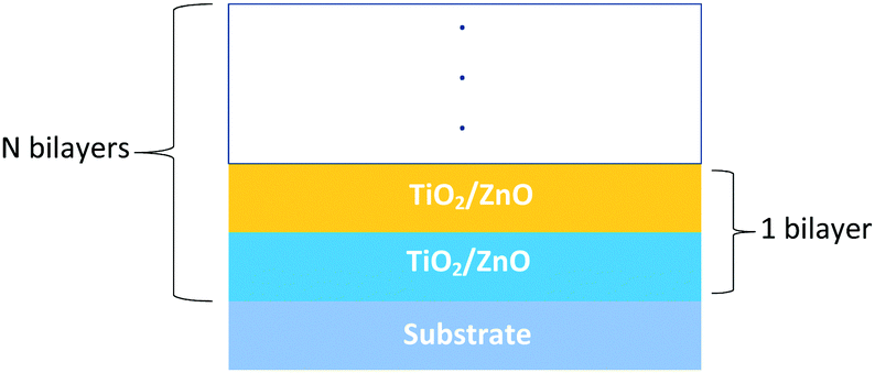 | ||
| Fig. 1 Schematic of the TiO2/ZnO nanolaminates. | ||
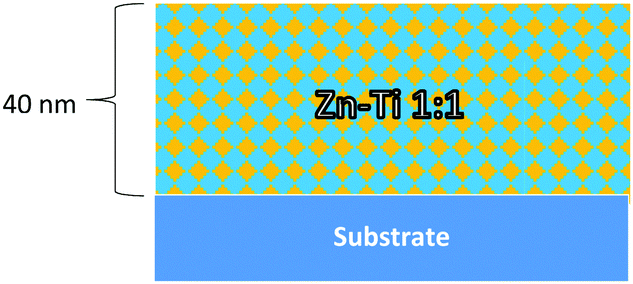 | ||
| Fig. 2 Schematic of the true ZnO:TiO2 1:1 nanolaminate. | ||
Experimental
Preparation of TiO2/ZnO composites
TiO2/ZnO bilayer laminate films were deposited on glass and Si(100) substrates using a Cambridge Nanotech Fiji 200 ALD system. Diethyl zinc (DEZn) (min. 95% Strem Chemicals), tetrakis(dimethylamido)titanium(IV) (TDMAT) (99% Strem Chemicals) and water were used as precursors at a growth temperature of 200 °C. Argon (Ar) was used a carrier gas to transport the precursor molecules into the chamber. During the deposition process, the diethyl zinc and water were sustained at room temperature while the temperature of the titanium precursor container; was set to a temperature of 80 °C to ensure sufficient vapour pressure was generated. Pulse times were 0.4 s, 0.2 s and 0.1 s for TDMAT, diethyl zinc and water respectively accompanied with a 10 s argon purge between precursor pulses to remove redundant ligands. The deposition rate was controlled at 2 Å per cycle for ZnO layers and 0.5 Å per cycle for TiO2 layers. The deposition depth of both ZnO and TiO2 layers was 40 nm. Films were produced with ZnO layer (40 nm) followed by TiO2 layer (40 nm) and vice versa. For comparison, TiO2 and ZnO films were grown with a thickness of 40 nm using the same precursors already mentioned. A laminate consisting of ZnO and TiO2 multilayers, (4 nm ZnO + 4 nm TiO2) ×5 was grown. A deliberately mixed ZnO/TiO2 1:1 film was also grown by alternating very short (0.05 s) pulses of each precursor until the desired thickness of 40 nm was reached.
Characterization techniques
The surface morphology of the film was observed using scanning electron microscopy (SEM) using a FEI Quanta 650 FEG High Resolution Scanning Electron Microscope. The crystallinity of the TiO2/ZnO films was analysed by X-ray diffraction (XRD) using a PANalytical X’Pert Pro diffractometer, with Cu Kα (λ = 0.154 nm) radiation from 10 to 70° at a step size of 0.02° under 45 kV and 30 mA. Grazing incidence XRD (GIXRD) was carried out on a Rigaku Ultima with an incidence angle of 2°. The XRD results were compared to the Joint Committee on the Powder Diffraction Standard cards (JPCDS). The interface of the bilayer was observed using transmission electron microscopy using FIB/TEM (JEOL JEM 2100). Atomic Force Microscopy (AFM) measurements were carried out in the non-contact mode, with an XE-100 apparatus from Park Systems, using sharp tips. The topographical 3D AFM images were taken over the area of 1 × 1 μm2. The images were processed with XEI (v.1.8.0) Image Processing Program developed by Park Systems. The UV-Vis transmission spectra were recorded in the range of 200–1000 nm using a PerkinElmer Lambda 950 UV/VIS/NIR spectrometer. The composition and binding energies of the films were investigated by X-ray photoelectron spectroscopy (XPS) using a Kratos AXIS_ULTRA spectrometer with the following parameters; sample temperature: 20–30 °C and X-ray gun: mono Al Kα 1486.58 eV; 150 W (10 mA, 15 kV). Samples were sputtered with Argon Gas Cluster source (10 keV, Ar1000+ clusters) for 2–3 s in order to remove the carbon over layer contact angle (CA) measurements were obtained using a Data Physics OCA 15EC system utilising a sessile drop arrangement at room temperature. A Hamilton 100 μL syringe was used to dispense 1 μL water droplets onto the surface. Small volumes were beneficial to avoid gravity-induced drop shape alteration and to diminish evaporation effects during CA measurements.Evaluation of photocatalytic activity
The photocatalytic activity was evaluated by degradation of dye under UV light irradiation. A dropper was used to add the dye of choice to the top of the film and a metal rod (3 mm K-bar) was used to spread the dye across the film. The dye was allowed to dry and subsequently exposed to UV light (3.30 mV cm−2). A qualitative approach was applied to monitor and record the dye degradation over time which involved the use of a handheld digital scanner.Results and discussion
The surface morphologies and structural properties of TiO2/ZnO films
Fig. 3 shows the GIXRD pattern of selected samples. For both ZnO grown on TiO2 and vice versa, the most predominate peaks can be attributed to hexagonal ZnO with the (002) peak being most evident. Strong preferential orientation for (002) indicates the polycrystalline manner of the ZnO film. This corresponds to wurtzite ZnO. On glass substrates, peaks are again visible for hexagonal ZnO but interestingly also seen are peaks that may be attributed to anatase TiO2. The GIXRD patterns suggest that ZnO is somewhat crystalline. Interestingly, the XRD pattern of both ZnO:TiO2 (1:1) and ZnO–TiO2 (bilayer ×5) appear to be strikingly similar on both glass and Si(100) substrates. A crystalline peak at approximately 52° on the Si(100) substrate is seen for both films and is assigned to TiO2(105), indicative of the anatase phase. The observed GIXRD peaks compare to standard JCPDS file data.
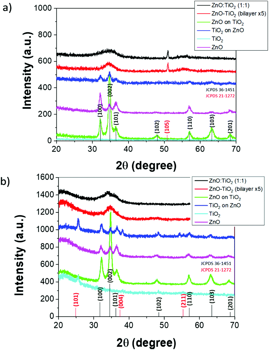 | ||
| Fig. 3 GIXRD patterns recorded from TiO2 (light blue), ZnO (pink), TiO2 on ZnO (dark blue) and ZnO on TiO2 (green), ZnO–TiO2 ×5 bilayer (red) and ZnO:TiO2 1:1 (black) grown on (a), an oxide-covered Si(100) substrate and (b), glass substrates. See insert caption for detail. | ||
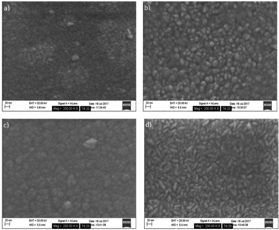
SEM reveals that the underlying structure of the ZnO layer affects the structure of the TiO2 grown on top. This can be seen by comparing the morphology of TiO2 grown directly on the substrate versus TiO2 grown on ZnO (Fig. 4 and 5). The morphology is comparable to ZnO. Growth also appears to be substrate-dependent based on the SEM images obtained. A difference can be seen between TiO2 deposited on (a), the oxide-covered Si(100) substrates and (b), the glass substrates. Larger surface features are evident on the glass substrate. These data are analysed further in a later section.
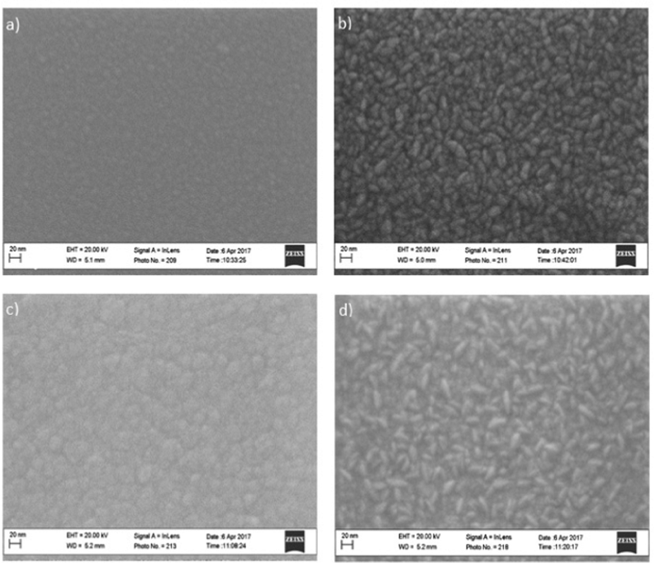 | ||
| Fig. 4 SEM images following ALD growth on Si(100) substrates: (a) TiO2 (b) ZnO (c) TiO2 on ZnO and (d) ZnO on TiO2. | ||
 | ||
| Fig. 5 SEM images following ALD growth glass substrates: (a) TiO2 (b) ZnO (c) TiO2 on ZnO and (d) ZnO on TiO2. | ||
The Scherrer eqn (1) was applied which relates the full width at half maximum height (FWHM) for the XRD peaks to the grain size.
 | (1) |
| Thin film | Scherrer method crystallite size (nm) | Intercept method crystallite size (nm) | |
|---|---|---|---|
| ZnO on TiO2 | Si | 12.1 | 22.7 |
| Glass | 12.0 | 21.9 | |
| TiO2 on ZnO | Si | 14.9 | 29.3 |
| Glass | 15.0 | 29.5 |
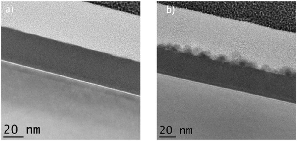
Transmission electron microscopy (TEM) images are presented in Fig. 6. In these images the darker layer is ZnO and the lighter layer is TiO2. The brighter layer seen below the TiO2 is a SiO2 interfacial layer as the Si(100) substrate is naturally oxidized. From Fig. 6(a) it is seen that the ZnO layer is thinner than the TiO2 layer despite the fact that the nominal growth rate of 2 Å per cycle was expected for ZnO and 0.5 Å per cycle for TiO2 which should have resulted in both layers having thicknesses of 40 nm. From the TEM images measured layer thicknesses of 35 nm for ZnO and 55–60 nm for TiO2 were obtained. This observation suggests that there was a delay in the nucleation of the ZnO layer at the start of the ALD growth process. It is possible that ZnO may self-inhibit when growing on Si and as a result there may be a need to fine tune the recipe to correct this discrepancy.
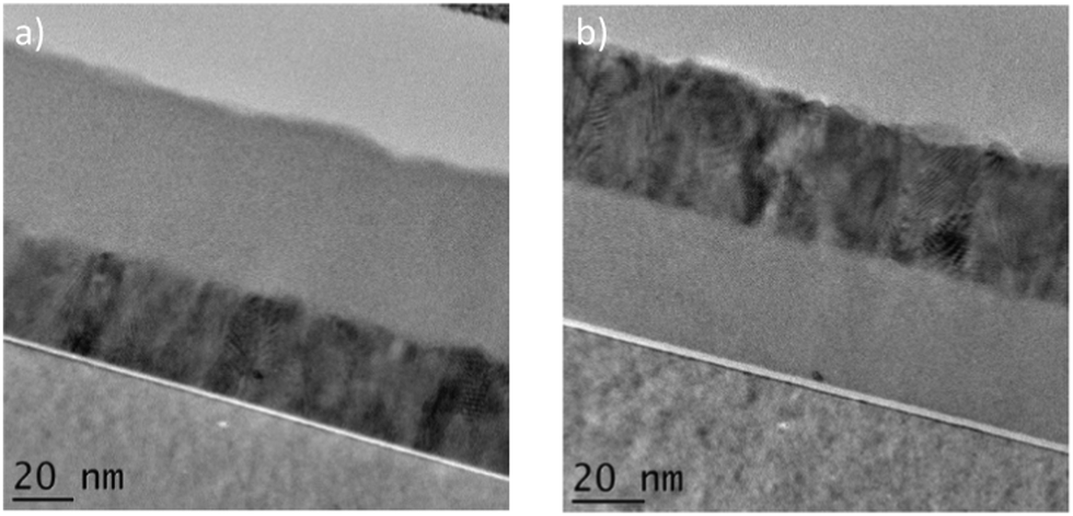 | ||
| Fig. 6 (a) TEM images of (a) the Si(100)/ZnO/TiO2 and (b) the Si(100)/TiO2/ZnO bilayer structures grown on the naturally-oxidized Si(100) substrates. Note the differences in layer thickness for the darker, ZnO layers when comparing both structures. | ||
In support of this proposal it is apparent that in contrast to the SiO2/ZnO/TiO2 structure, the SiO2/TiO2/ZnO structure shows similar layer thicknesses for the TiO2 and ZnO layers, Fig. 6(b). From these TEM images it is evident that ZnO is crystalline due to clear lattice plane images being present in the TEM image and TiO2 is amorphous which explains why no diffraction peaks were obtained in the XRD pattern on Si substrate.
Fig. 7 shows TEM images of true nanolaminate films. Again, the darker layers represent ZnO and the lighter coloured layers represent TiO2. The nanolaminate remains intact and the layers can clearly be distinguished. In support of the earlier proposal that the growth of the ZnO on the oxidized Si(100) surface is somewhat inhibited, from Fig. 7 it is possible to see clearly that the first of the very thin ZnO layers simply did not grow due to the proposed delay in nucleation. Interestingly in this example, the TiO2 layers were thicker than expected, being some 6 nm as opposed to the expected 4 nm. The GPC of TiO2 grown on ZnO appears to be greater than that of pure TiO2 deposited directly on substrate. The opposite is observed with ZnO where the GPC of ZnO deposited on TiO2 is reduced compared to that of pure ZnO grown directly on the substrate. This may be explained by considering surface chemisorption reactions. ALD is very sensitive to the chemical activity of the growth surface. Differences may exist in the chemical activity of the TDMAT and DEZn precursors and these differences could explain the resulting GPC values. A similar result has been observed in other ALD experiments.57,58
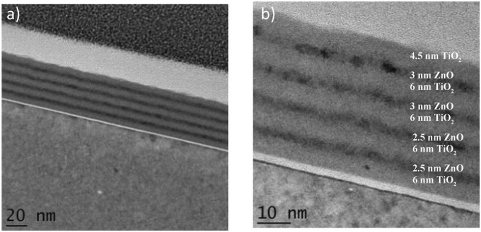 | ||
| Fig. 7 TEM images of ZnO and TiO2 multilayers laminate (4 nm ZnO + 4 nm TiO2) ×5 at (a) 20 nm and (b) 10 nm. | ||
As seen in Fig. 8 the TEM images of the mixed ZnO/TiO2 (1:1) layer reveal that after annealing some new deposits appear at the surface of the layer which also appears to have reduced in overall thickness from roughly 32 nm to 29 nm. Given the tendency of ZnO to readily form crystalline deposits it is proposed that the new deposits consisted on ZnO nanocrystals that form via segregation of Zn2+ ions from the mixed layer, oxidation and crystallisation. With this proposal in mind ZnO lattice constants were calculated in accordance with Bragg's law59 Using 1.54 Å for λ (Cu Kα radiation). The values for d; the interplanar spacing for ZnO(002) and (100) orientations are 2.68 Å and 2.9 Å respectively, confirming that the deposits were most likely ZnO nanocrystals having a predominant orientation on the (002) direction as the interplanar spacing measurement was in agreement with the theoretical value. It has previously been reported that annealing ALD ZnO produces films preferentially oriented with the c-axis perpendicular to the substrate.60,61Fig. 9 shows the interplanar spacing within the ZnO nanocrystals as observed using TEM.
 | ||
| Fig. 8 TEM images of the mixed 1:1 ZnO:TiO2 (1:1) layer (a) before and (b) after, annealing at 400 °C for 60 minutes in air. | ||
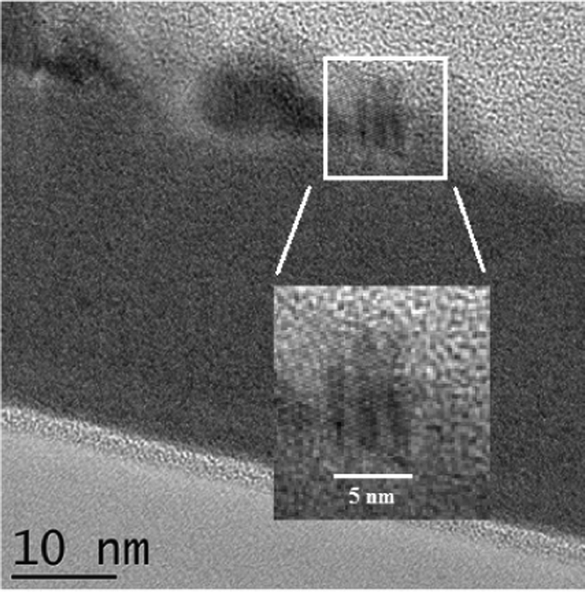 | ||
| Fig. 9 TEM image of the annealed mixed ZnO/TiO2 layer focusing on one of the deposits that appear at the surface of the layer after annealing at 400 °C for 60 minutes in air. | ||
Atomic force microscopy (AFM) was employed to evaluate the surface topography of the ZnO, TiO2 and ZnO/TiO2 nanolaminate films. AFM images recorded for all films are presented in Fig. 10. The sampling surface area of the films analysed was 1 × 1 μm2. The lighter coloured areas in the images indicate higher surface features. The Z scale of the AFM data is situated to the left of each image. The Z scale values vary from sample to sample with a maximum of >20 nm for ZnO deposited on TiO2 on glass substrate.
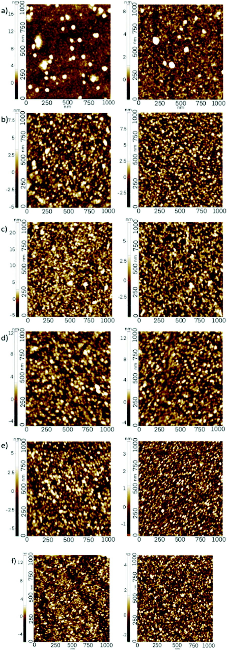 | ||
| Fig. 10 AFM images of (a) TiO2, (b) ZnO, (c) ZnO on TiO2, (d) TiO2 on ZnO, (e) mixed ZnO:TiO2 (1:1) layer and, (f) ×5 bilayers. | ||
The RMS roughness was evaluated for each of the films. These results are displayed in Table 2. It can be seen from the results that RMS roughness increases for all films grown on glass substrates when compared to the same films deposited on Si substrate. This supports the proposal that growth is substrate-dependent as previously implied from the XRD results. Comparing TiO2 and TiO2 grown on ZnO, the RMS roughness values are practically the same on glass substrates, at ca. 1.49 nm and 1.5 nm respectively. However, the RMS roughness value doubles in the case of growth on the Si(100) substrate from 0.64 nm for TiO2 alone to 1.2 nm for TiO2 grown onto ZnO on Si(100). In other words the surface of the TiO2 layer is considerably rougher when deposited onto ZnO grown on Si(100) as compared to that obtained when the TiO2 was deposited directly on the Si(100) substrate.
| RMS roughness of films grown on glass substrates (nm) | RMS roughness of films grown on Si(100) substrates (nm) | |
|---|---|---|
| ZnO | 1.49 | 0.64 |
| TiO2 | 1.68 | 1.27 |
| ZnO on TiO2 | 1.77 | 1.64 |
| TiO2 on ZnO | 1.50 | 1.21 |
| ZnO:TiO2 (1:1) mixed layer |
1.63 | 0.61 |
| ZnO/TiO2 ×5 | 1.24 | 0.80 |
Comparing ZnO and ZnO deposited onto TiO2, again the RMS roughness values are very similar on glass substrates although a slight increase in RMS roughness is observed when the ZnO is deposited onto the TiO2 layer grown on glass, having a slightly larger value at 1.77 nm as compared to 1.68 nm. Similarly the RMS roughness value obtained from the surface of the ZnO layer deposited onto the TiO2 layer grown on the Si(100) substrate is again higher than that for ZnO grown directly on the Si(100) substrate, at 1.64 nm versus 1.27 nm, although the increase in RMS roughness isn’t as substantial as that observed for the TiO2 layer. For the nanolaminate stacks, RMS roughness values were found to be lower in comparison to the other films, being ca. 1.24 nm on glass and 0.8 nm on Si(100).
Interestingly, the mixed ZnO/TiO2 1:1 layer grown on a glass substrate had one of the highest results in terms of RMS roughness, at ca. 1.63 nm. In contrast, the same structure grown on the Si(100) substrate had one of the lowest RMS roughness values, at ca. 0.61 nm.
Fig. 10 below present AFM images for the nanolaminate films. For all images, films deposited on glass substrates are the left and films deposited on Si(100) substrates are on the right.
XPS was employed to characterise the chemical bonding and composition of the films. Fig. 11(a)–(c) show the XPS spectra of the Ti 2p, Zn 2p and O 1s peaks after mild argon-ion sputtering designed to remove the surface contamination that arises due to handling in air. The major doublet peaks at 459 eV and 465 eV in Fig. 11(a) can be assigned to Ti 2p3/2 and Ti 2p1/2 peaks of Ti–O bonding, consistent with the literature that exists for TiO2.48,62,63 The spectra can also be fitted with a second doublet at Ti 2p3/2 at approx. 457.5 eV which can be attributed to Ti(III) oxide and hence Ti3+.62,63 The 2 peaks seen in Fig. 11(b) at 1021 eV and 1044 eV correspond to Zn 2p3/2 and Zn 2p1/2 and corresponds to accepted XPS data for ZnO found in the literature.48 The O 1s spectrum depicted in Fig. 11(c) shows a peak at 529 eV which is attributed to oxygen bound to metal ions in the form of Ti–O and Zn–O species.48
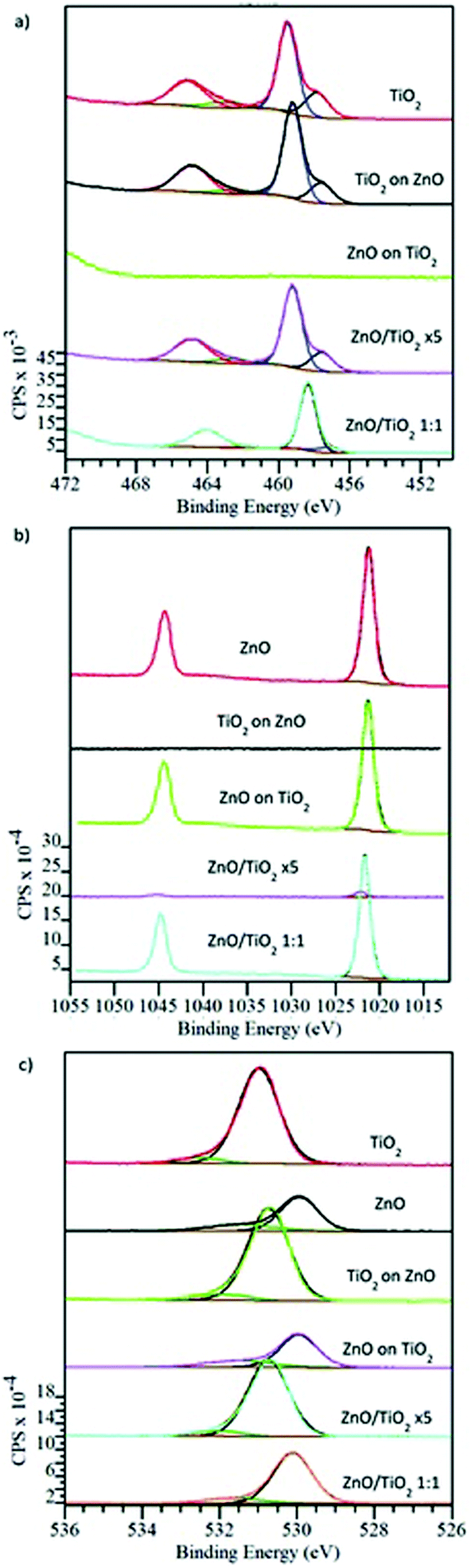 | ||
| Fig. 11 XPS spectra on Si(100) substrates of (a) Ti 2p for TiO2, TiO2 on ZnO, ZnO on TiO2, ZnO/TiO2 ×5 and ZnO:TiO2 (1:1) (b) Zn 2p for ZnO, TiO2 on ZnO, ZnO on TiO2, ZnO/TiO2 ×5 and ZnO:TiO2 (1:1) and (c) O 1s for TiO2, ZnO TiO2 on ZnO, ZnO on TiO2, ZnO/TiO2 ×5 and ZnO:TiO2 (1:1). | ||
The XPS data are entirely consistent with the growth of the target materials and do not indicate that layers are deficient in terms of any particular species. However, for the films which terminate in a TiO2 layer, or for the deliberately mixed films, XPS can be particularly useful as a means of detecting Ti3+ species which have been reported to play a crucial role in determining the photocatalytic activity of the film. Ti3+ formation may arise from oxygen vacancies created as a result of oxygen diffusion.64Table 3 lists the percentage of Ti3+ present in the TiO2 only film, the ZnO/TiO2 ×5 nanolaminate stack, the ZnO/TiO2 bilayer nanolaminate and the ZnO:TiO2 (1:1) as determined from the Ti 2p XPS data:
| Sample | % Ti3+ |
|---|---|
| TiO2 | 25.6 |
| ZnO/TiO2 ×5 | 21.9 |
| TiO2 on ZnO | 20.5 |
| ZnO:TiO2 (1:1) |
8.8 |
From Table 3 it may be seen that the layered nanolaminate structures has 20–25% of the titanium present as Ti3+ and the rest as Ti4+. These surfaces may provide photogenerated hole traps and assist with enhancing photocatalytic activity. Hole traps can increase the excited electron lifetimes located near the surface oxide species. This offers an opportunity for a greater chance of surface reactive oxide species (ROS) generation.65–67 This will be further discussed in terms of photocatalytic activity later. However, mixed nanolaminate ZnO:TiO2 (1:1) is seen to behave differently that it has a lower relative concentration of Ti3+ and Ti 2p3/2 peak of the dominant Ti(IV) oxide is shifted to a lower binding energy of 458.3 eV suggesting that the immediate chemical/structural environment of the Ti4+ is different to that of the other layered TiO2 nanolaminates.
Optical properties
The optical transmittance spectra for ZnO:TiO2 (1:1), ZnO/TiO2 (×5 bilayer), ZnO/TiO2 and TiO2/ZnO bilayer nanolaminate structures grown on glass can be seen in Fig. 12. The average transmittance over the entirety of the visible wavelength range 400 to 550 nm is >60% rising to a maximum of ∼80% at 400 nm for the TiO2 on ZnO sample and to ∼90% for the ZnO on TiO2 sample. At 380 nm, a strong absorption peak is evident due to the fundamental band gaps of the materials. A slight bump is seen at 350 nm which may be a consequence of the film being a composite of two separate layers. The transmittance values for both films decline to ∼0% at lower wavelengths due to near complete absorption in the UV region. The ZnO/TiO2 and TiO2/ZnO bilayer nanolaminates absorb more strongly in the UV/visible region in comparison to the ZnO:TiO2 (1:1) and ZnO/TiO2 (×5 bilayer) films. A blue shift in the wavelength of the absorption edge is observed with the ZnO:TiO2 (1:1) and ZnO/TiO2 (×5 bilayer) films with ZnO:TiO2 (1:1) possessing the greatest effect on the shift. The blue shift observed may be explained by the Burstein–Moss effect. In this instance, the optical band gap of a semiconductor is increased with increasing electron concentration as the conduction band is occupied with excited electrons. The bottom of the conduction band is filled with donor electrons. According to Pauli's principle no two electrons may occupy the same state hence leading to a blockage in low-energy transitions which in turn enhances the optical band gap.68 The structure of the latter films resemble that of Ti-doped ZnO (TZO). Hence, the carrier concentration may effectively be increased as Ti could be behaving as a donor material.
 | ||
| Fig. 12 Transmittance spectra of the ZnO:TiO2 (1:1), ZnO/TiO2 (×5 bilayer), ZnO/TiO2 bilayer nanolaminate structures grown on glass. | ||
Contact angle and photocatalytic activity
Contact angle (CA) measurements were taken in order to get an idea of the hydrophilic or hydrophobic nature of the films. In general a low surface energy and a rough microstructure equate to super-hydrophobicity.69 The CA was measured prior to UV exposure, after 30 minutes and after 1 hour UV exposure. All values displayed are taken from films that had been annealed at 400 °C for 1 hour in air.Initially, films grown on the glass substrates had lower CAs than those grown on Si(100) substrates. In some ways this would not be unexpected since XRD revealed that on these samples there was evidence of anatase formation and anatase is generally found to be the most photoactive form of TiO2.70 Following 30 minutes UV irradiation, the CAs decreased for all samples except for the TiO2 on ZnO grown on glass sample (Fig. 13) and for ZnO/TiO2 (×5 bilayers) grown on Si (Fig. 14). After 1 hour UV exposure, the CA for TiO2 on ZnO grown on glass increased dramatically. Out of all the samples, the CAs for the ZnO:TiO2 (1:1) films were found to be the some of the highest, however a slight decrease in CA with increasing irradiation time was observed. CAs of <5° were recorded for TiO2 on glass after UV exposure which is indicative of superhydrophilicity. This is again indicative of some photoactivity arising from the presence of some anatase. Although no general consensus exists to explain why, amorphous TiO2 surfaces are not found to be particularly photoactive while anatase surfaces are the most photoactive.70
 | ||
| Fig. 13 Contact angle measurements for TiO2 and TiO2 on ZnO grown on both Si(100) and glass substrates, after annealing at 400 °C for 1 hour in air and then exposed to UV radiation, as a function of time. | ||
 | ||
| Fig. 14 Contact angle measurements for ZnO/TiO2 (×5 bilayers) and ZnO:TiO2 (1:1) grown on both Si(100) and glass substrates, after annealing at 400 °C for 1 hour in air and then exposed to UV radiation, as a function of time. | ||
Morphological influences may also influence CA values. In our case particularly if the TiO2 adopts the shape of the ZnO grown directly beneath it as in the case of the TiO2 on ZnO grown on Si(100) substrate sample (see Fig. 4(c)). The CA data for this sample is shown in the red solid line in Fig. 13 and reveals that the CA remains high despite UV irradiation for an hour. In this particular case it would be tempting to assume that the very prominent texturing of the TiO2 surface that arises from the ZnO template underneath dominates the CA response completely. However a similar level of texturing, albeit less uniform in nature, arises for TiO2 on ZnO grown on a glass substrate and as may be seen from the red dotted line in Fig. 13 this material has a low CA value to start with which actually increases during UV exposure. Such potentially conflicting results are indicative of the fact that CA measurements are at best only a very rough guide to wards understanding the hydrophobicity or hydrophilicity of a sample surface.
Photocatalytic activity was also investigated via dye degradation experiments. Films were coated with an even layer of basic blue 66 dye and exposed to UV light and the change in the colour of the ink was monitored and recorded over time by use of a handheld digital scanner. Digital image analysis as described by Mills et al. was used to assess photo-activity of the films.71
Fig. 15 below shows the films initially covered with a thin layer of dye before UV exposure and after 150 minutes of UV bleaching.
 | ||
| Fig. 15 Images of the samples before and after 150 minutes UV irradiation on glass substrate: (a) TiO2 (b) ZnO (c) TiO2 on ZnO (d) ZnO on TiO2 (e) ZnO/TiO2 ×5 and (f) ZnO:TiO2 (1:1).† | ||
By comparing the before and after images presented in Fig. 15, it is concluded that the dye did not degrade to any visual degree on the ZnO/TiO2 ×5 nanolaminate stack grown on glass suggesting nearly complete inactivity (samples (e) in Fig. 15). For the samples shown in (c) in these figures which were the ZnO/TiO2 bilayer samples grown on glass with the TiO2 layer on top of the ZnO layer, the dye only showed slight discolouration suggesting that this sample had some, albeit minimal levels of photoactivity.
Comparing the samples shown in (c) TiO2 on ZnO and (d) ZnO on TiO2 (c) in these figures, the dye was again degraded suggesting that these films also possessed some degree of photoactivity. Similarly the samples shown in (f) also degraded the dye to some extent showing photoactivity.
Although some of the films display some degree of photoactivity, the shortest time-to-bleach as determined by visual inspection was around 69 minutes exposure.
By assessment of the time-to-bleach values given in Table 4, it may be seen that the ZnO and TiO2 films are the most photoactive, followed closely by ZnO:TiO2 (1:1). A value for the time to bleach ZnO/TiO2 ×5 bilayer could not be calculated.
:TiO2 (1:1) films
The results from the dye degradation experiments are in good agreement with the CA values obtained for the films after 1 hour UV exposure. Interestingly, XPS results revealed that the TiO2 on ZnO film contained the highest percentage of Ti3+ on its surface. However, CA and dye degradation experiments suggest that this film is not particularly photoactive. The presence of Ti3+ influences the electronic structure and surface activity of TiO2.72 In particular it is likely that the presence of Ti3+ extends the wavelength range where the material absorbs into the visible region of the spectrum. If this were the case then it might provide a mechanism whereby the visible light-induced photocatalytic activity could become significant.73–77 However as noted above, these samples were not found to be photoactive using the tests employed.
Conclusions
TiO2/ZnO nanolaminates were deposited via an ALD process which revealed a slight delay in nucleation with ZnO. SEM showed that TiO2 morphology follows that of the ZnO underneath. XRD results suggested that layer growth was substrate-dependent as crystalline TiO2 was only identified on glass. The ZnO was polycrystalline as evidenced by the appearance lattice fringes in the TEM images while the TiO2 was amorphous. TEM revealed that the laminates remained intact after annealing. Nanocrystals were seen on top of the mixed Zn:Ti (1:1) film and thus it is apparent that the mixed film is not stable towards high temperature annealing. These results suggest that formation of a nanolaminate structure may help with stability. After 1 hour UV exposure, the TiO2 yielded a CA value of <5°, suggesting superhydrophilicity.
This study highlights how the use of an underlayer may act as a template of morphology. It also suggests the possible role of nanolaminates in stabilizing materials. In a practical sense, TiO2 may act as a stabilizer for ZnO in a TiO2/ZnO bilayer stack when used as an anode material in lithium ion batteries (LIBs).78
Author contributions
S. D. fabricated nanolaminate films, carried out; SEM analysis (supervised by Vincent Lodge at Tyndall National Institute), optical measurements, contact angle measurements and photocatalytic activity experiments (supervised by Harry Manley at Tyndall National Institute). S. D. also prepared the manuscript. L. R. and M. M. M. fabricated nanolaminate films. M. M. carried out GIXRD and AFM analysis. M. S. carried out FIB/TEM analysis. F. L. carried out the XPS analysis. All authors have given approval to the final version of the manuscript.Conflicts of interest
There are no conflicts to declare.Acknowledgements
This work forms part of the research currently underway at Tyndall funded by Science Foundation Ireland (SFI) Principal Investigator Project number 15/IA/3015 ‘Design, Deposition and Exploitation of Novel Micro and Nano-scale Materials and Devices for Advanced Manufacturing – DEPO-Man’. The author gratefully acknowledges the support of the Irish Research Council GOIPG/2016/990.Notes and references
- B. Radisavljevic, A. Radenovic, J. Brivio, V. Giacometti and A. Kis, Single-layer MoS2 transistors, Nat. Nanotechnol., 2011, 6(3), 147–150 CrossRef CAS PubMed.
- O. Lopez-Sanchez, D. Lembke, M. Kayci, A. Radenovic and A. Kis, Ultrasensitive photodetectors based on monolayer MoS2, Nat. Nanotechnol., 2013, 8(7), 497–501 CrossRef CAS PubMed.
- S. Bertolazzi, J. Brivio and A. Kis, Stretching and Breaking of Ultrathin MoS2, ACS Nano, 2011, 5(12), 9703–9709 CrossRef CAS PubMed.
- H. Zeng, J. Dai, W. Yao, D. Xiao and X. Cui, Valley polarization in MoS2 monolayers by optical pumping, Nat. Nanotechnol., 2012, 7, 490–493 CrossRef CAS PubMed.
- W. Zhang, C. P. Chuu, J. K. Huang, C. H. Chen, M. L. Tsai, Y. H. Chang, C. T. Liang, Y. Z. Chen, Y. L. Chueh, J. H. He, M. Y. Chou and L. J. Li, Ultrahigh-Gain Photodetectors Based on Atomically Thin Graphene-MoS2 Heterostructures, Sci. Rep., 2014, 23(4), 3826 Search PubMed.
- C. Cong, J. Shang, X. Wu, B. Cao, N. Peimyoo, C. Qiu, L. Sun and T. Yu, Synthesis and Optical Properties of Large-Area Single-Crystalline 2D Semiconductor WS2 Monolayer from Chemical Vapor Deposition, Adv. Opt. Mater., 2014, 2, 131–136 CrossRef.
- Y. Cai, J. Lan, G. Zhang and Y. W. Zhang, Lattice vibrational modes and phonon thermal conductivity of monolayer MoS2, Phys. Rev. B: Condens. Matter Mater. Phys., 2014, 89, 035438 CrossRef.
- J. Azadmanjiri, C. C. Berndt, J. Wang, A. J. Kapoor and V. K. Srivastavac, Nanolaminated composite materials: structure, interface role and applications, RSC Adv., 2016, 6, 109361 RSC.
- P. Sundberg and M. Karppinen, Organic and inorganic-organic thin film structures by molecular layer deposition: a review, Beilstein J. Nanotechnol., 2014, 5, 1104–1136 CrossRef PubMed.
- D. F. Schmidt, Nanolaminates - Bioinspired and beyond, Mater. Lett., 2013, 108, 328–335 CrossRef CAS.
- J. Azadmanjiri, C. C. Berndt, J. Wang, A. J. Kapoor, V. K. Srivastavac and C. Wen, A review on hybrid nanolaminate materials synthesized by deposition techniques for energy storage applications, J. Mater. Chem. A, 2014, 2, 3695–3708 RSC.
- M. Puttaswamy, M. Vehkamäki, K. Kukli, M. C. Dimri, M. Kemmel, T. Hatanpää, M. J. Heikkilä, K. Mizohata, R. Stern, M. Ritala and M. Leskelä, Bismuth iron oxide thin films using atomic layer deposition of alternating bismuth oxide and iron oxide layers, Thin Solid Films, 2016, 611, 78–87 CrossRef CAS.
- G. Zhang, H. Wu, X. Wang, D. Zhang, T. Wang and C. Liu, Modulation of the dissipation factor in transparent AlZnO/ZrO2/AlZnO capacitors, J. Alloys Compd., 2017, 690, 777–782 CrossRef CAS.
- J. R. Martínez-Castelo, J. López, D. Domínguez, E. Murillo, R. Machorro, H. A. Borbón-Nuñez, I. Fernandez-Alvarez, A. Arias, M. Curiel, N. Nedev, M. H. Farías and H. Tiznado, Structural and electrical characterization of multilayer Al2O3/ZnO nanolaminates grown by atomic layer deposition, Mater. Sci. Semicond. Process., 2017, 71, 290–295 CrossRef.
- T. Onaya, T. Nabatame, T. Sawada, K. Kurishima, N. Sawamoto, A. Ohi and A. Ogura, Improved leakage current properties of ZrO2/(Ta/Nb)Ox -Al2O3/ZrO2 nanolaminate insulating stacks for dynamic random access memory capacitors, Thin Solid Films, 2018, 655, 48–53 CrossRef CAS.
- W. Chen, W. Ren, Y. Zhang, M. Liu and Z. G. Ye, Preparation and properties of ZrO2 and TiO2 films and their nanolaminates by atomic layer deposition, Ceram. Int., 2015, 41, S278–S282 CrossRef CAS.
- A. Rodríguez, M. B. Gonzalez, F. Campabadal, J. Suñé and E. Miranda, Electrical characterization of multiple leakage current paths in HfO2/Al2O3-based nanolaminates, Microelectron. Reliab., 2015, 55(9-10), 1442–1445 CrossRef.
- H. Cho, K. W. Park, C. H. Park, H. J. Cho, S. J. Yeom, K. Hong, N. J. Kwak and J. H. Ahn, Abnormally enhanced dielectric constant in ZrO2/Ta2O5 multi-laminate structures by metallic Ta formation, Mater. Lett., 2015, 154, 148–151 CrossRef CAS.
- J. López, J. Martínez, N. Abundiz, D. Domínguez, E. Murillo, F. Castillón, R. Machorro, M. Farías and H. Tiznado, Thickness effect on the optical and morphological properties in Al2O3/ZnO nanolaminate thin films prepared by atomic layer deposition, Superlattices Microstruct., 2016, 90, 265–273 CrossRef.
- R. Lo Nigro, E. Schilirò, G. Greco, P. Fiorenza and F. Roccaforte, Laminated Al2O3–HfO2 layers grown by atomic layer deposition for microelectronics applications, Thin Solid Films, 2016, 601, 68–72 CrossRef CAS.
- C. Mahata, Y. An, S. Choi, Y. C. Byun, D. K. Kim, T. Lee, J. Kim, M. H. Cho and H. Kim, Electrical properties of the HfO2–Al2O3 nanolaminates with homogeneous and graded compositions on InP, Curr. Appl. Phys., 2016, 16(3), 294–299 CrossRef.
- J. Zhang, X. Ding, J. Li, H. Zhang, X. Jiang and Z. Zhang, Performance enhancement in InZnO thin-film transistors with compounded ZrO2–Al2O3 nanolaminate as gate insulators, Ceram. Int., 2016, 42(7), 8115–8119 CrossRef CAS.
- J. Gao, G. He, Z. Sun, H. Chen, C. Zheng, P. Jin, D. Xiao and M. Liu, Modification of electrical properties and carrier transportation mechanism of ALD-derived HfO2/Si gate stacks by Al2O3 incorporation, J. Alloys Compd., 2016, 667, 352–358 CrossRef CAS.
- A. Rodriguez, M. B. Gonzalez, F. Campabadal, J. Suñé and E. Miranda, Breakdown time statistics of successive failure events in constant voltage-stressed Al2O3/HfO2 nanolaminates, Microelectron. Eng., 2015, 147, 85–88 CrossRef CAS.
- C. Mahata, Y. C. Byun, C. H. An, S. Choi, Y. An and H. Kim, Comparative study of atomic-layer-deposited stacked (HfO2/Al2O3) and nanolaminated (HfAlOx) dielectrics on In0.53Ga0.47As, ACS Appl. Mater. Interfaces, 2013, 5(10), 4195–4201 CrossRef CAS PubMed.
- L. H. Kim, K. Kim, S. Park, Y. J. Jeong, H. Kim, D. S. Chung, S. H. Kim and C. E. Park, Al2O3/TiO2 Nanolaminate Thin Film Encapsulation for Organic Thin Film Transistors via Plasma-Enhanced Atomic Layer Deposition, ACS Appl. Mater. Interfaces, 2014, 6, 6731–6738 CrossRef CAS PubMed.
- A. Singh, F. Nehm, L. Müller-Meskamp, C. Hoßbach, M. Albert, U. Schroeder, K. Leo and T. Mikolajick, OLED compatible water-based nanolaminate encapsulation systems using ozone based starting layer, Org. Electron., 2014, 15, 2587–2592 CrossRef CAS.
- J. Oh, S. Shin, J. Park, G. Ham and H. Jeon, Characteristics of Al2O3/ZrO2 laminated films deposited by ozone-based atomic layer deposition for organic device encapsulation, Thin Solid Films, 2016, 599, 119–124 CrossRef CAS.
- E. G. Jeong, Y. C. Han, H. G. Im, B. S. Bae and K. C. Choi, Highly reliable hybrid nano-stratified moisture barrier for encapsulating flexible OLEDs, Org. Electron., 2016, 33, 150–155 CrossRef CAS.
- F. Nehm, F. Dollinger, H. Klumbies, L. Müller-Meskamp, K. Leo, A. Singh, C. Richter, U. Schroeder, T. Mikolajick, C. Hossbach, M. Albert and J. W. Bartha, Atomic layer deposited TiOx/AlOx nanolaminates as moisture barriers for organic devices, Org. Electron., 2016, 38, 84–88 CrossRef CAS.
- J. Leppäniemi, P. Sippola, M. Broas, J. Aromaa, H. Lipsanen and J. Koskinen, Corrosion protection of steel with multilayer coatings: Improving the sealing properties of physical vapor deposition CrN coatings with Al2O3/TiO2 atomic layer deposition nanolaminates, Thin Solid Films, 2017, 627, 59–68 CrossRef.
- P. A. Radi, G. E. Testoni, R. S. Pessoa, H. S. Maciel, L. A. Rocha and L. Vieira, Tribocorrosion behavior of TiO2/Al2O3 nanolaminate, Al2O3, and TiO2 thin films produced by atomic layer deposition, Surf. Coat. Technol., 2018, 349, 1077–1082 CrossRef CAS.
- B. Díaz, E. Härkönen, J. Światowska, A. Seyeux, V. Maurice, M. Ritala and P. Marcus, Corrosion properties of steel protected by nanometre-thick oxide coatings, Corros. Sci., 2014, 82, 208–217 CrossRef.
- E. Härkönen, S. Tervakangas, J. Kolehmainen, B. Díaz, J. Swiatowska, V. Maurice, A. Seyeux, P. Marcus, M. Fenker, L. Tóth, G. Radnöczi and M. Ritala, Interface control of atomic layer deposited oxide coatings by filtered cathodic arc deposited sublayers for improved corrosion protection, Mater. Chem. Phys., 2014, 147, 895–907 CrossRef.
- H. Mohseni and T. W. Scharg, Role of atomic layer deposited solid lubricants in the sliding wear reduction of carbon–carbon composites at room and higher temperatures, Wear, 2015, 332-333, 1303–1313 CrossRef CAS.
- J. López, H. A. Borbón-Nuñez, E. G. Lizarraga-Medina, E. Murillo, R. Machorro, N. Nedev and G. Soto, Al2O3 -Y2O3 ultrathin multilayer stacks grown by atomic layer deposition as perspective for optical waveguides applications, Opt. Mater., 2017, 72, 788–794 CrossRef.
- N. Pinna and M. Knez, Atomic Layer Deposition of Nanostructured Materials, Wiley-VCH: Weinheim, Germany, 2012 Search PubMed.
- H. B. Lee, V. R. Anderson and S. M. George, Growth and Properties of Hafnicone and HfO2/Hafnicone Nanolaminates and Alloy Films Using Molecular Layer Deposition Techniques, ACS Appl. Mater. Interfaces, 2014, 6, 16880–16887 CrossRef PubMed.
- M. Leskelä and M. Ritala, Atomic layer deposition (ALD): from precursors to thin film structures, Thin Solid Films, 2002, 409, 138–146 CrossRef.
- R. W. Johnson, A. Hultqvist and S. F. Bent, A brief review of atomic layer deposition: from fundamentals to applications, Mater. Today, 2014, 17(5), 236–246 CrossRef CAS.
- C. A. P. Handwerker and T. M. Pollock, Emerging Science and Research Opportunities for Metals and Metallic Nanostructures, JOM, 2014, 66(7), 1321–1341 CrossRef CAS.
- A. Janotti and C. G. Van de Walle, Fundamentals of zinc oxide as a semiconductor, Rep. Prog. Phys., 2009, 72, 126501 CrossRef.
- D. Reyes-Coronado, G. Rodríguez-Gattorno, M. E. Espinosa-Pesqueira, C. Cab, R. de Coss and G. Oskam, Phase-pure TiO2 nanoparticles: anatase, brookite and rutile, Nanotechnology, 2008, 19, 145605 CrossRef CAS PubMed.
- L. Xu, L. Shi and X. Li, Effect of TiO2 buffer layer on the structural and optical properties of ZnO thin films deposited by E-beam evaporation and sol-gel method, Appl. Surf. Sci., 2008, 255, 3230–3234 CrossRef CAS.
- J. Tian, L. Chen, Y. Yin, X. Wang, J. Dai, Z. Zhu, X. Liu and P. Wu, Photocatalyst of TiO2/ZnO nano composite film: Preparation, characterization, and photodegradation activity of methyl orange, Surf. Coat. Technol., 2009, 204, 205–214 CrossRef CAS.
- P. Prasannalakshmi and N. Shanmugam, Fabrication of TiO2/ZnO nanocomposites for solar energy driven photocatalysis, Mater. Sci. Semicond. Process., 2017, 61, 114–124 CrossRef CAS.
- Y. Z. Gu, H. L. Lu, Y. Geng, Z. Y. Ye, Y. Zhang, Q. Q. Sun, S. J. Ding and D. W. Zhang, Optical and microstructural properties of ZnO/TiO2 nanolaminates, Nanoscale Res. Lett., 2013, 8, 107 CrossRef PubMed.
- X. Qian, M. Y. Gao, Y. Q. Cao, B. L. Guo and A. D. Li, Preparation and phase structures of Zn–Ti–O ternary compounds by atomic layer deposition, J. Vac. Sci. Technol., A, 2013, 31 Search PubMed.
- W. K. Wang, H. C. Wen, C. H. Cheng, C. H. Hung, W. C. Chou, W. H. Yau, P. F. Yang and Y. S. Lai, Nanotribological properties of ALD-processed bilayer TiO2/ZnO films, Microelectron. Reliab., 2014, 54, 2754–2759 CrossRef CAS.
- R. Chen, J. L. Lin, W. J. He, C. L. Duan, Q. Peng and X. L. Wang, Spatial atomic layer deposition of ZnO/TiO2 nanolaminates, J. Vac. Sci. Technol., A, 2016, 34, 5 Search PubMed.
- A. Leelavathi, G. Madras and N. Ravishankar, Origin of enhanced photocatalytic activity and photoconduction in high aspect ratio ZnO nanorods, Phys. Chem. Chem. Phys., 2013, 15, 10795–10802 RSC.
- C. Han, M.-Q. Yang, B. Weng and Y.-J. Xu, Improving the photocatalytic activity and anti-photocorrosion of semiconductor ZnO by coupling with versatile carbon, Phys. Chem. Chem. Phys., 2014, 16, 16891–16903 RSC.
- W. Li, G. Wang, C. Chen, J. Liao and Z. Li, Enhanced Visible Light Photocatalytic Activity of ZnO Nanowires Doped with Mn2+ and Co2+ Ions, Nanomaterials, 2017, 7(1), 20 CrossRef PubMed.
- E. Rokhsat and O. Akhavan, Improving the photocatalytic activity of graphene oxide/ZnO nanorod films by UV irradiation, Appl. Surf. Sci., 2016, 371, 590–595 CrossRef CAS.
- P. Scherrer, Bestimmung der Größe und der inneren Struktur von Kolloidteilchen mittels Röntgenstrahlen, Nachr. Ges. Wiss. Goettingen, Math.-Phys. Kl., 1918, 98 Search PubMed.
- H. Abrams, Grain Size Measurement by the Intercept Method, Metallography, 1971, 4(1), 59–78 CrossRef.
- P. Poodt, A. Lankhorst, F. Roozeboom, K. Spee, D. Maas and A. Vermeer, High-Speed Spatial Atomic-Layer Deposition of Aluminum Oxide Layers for Solar Cell Passivation, Adv. Mater., 2010, 22(32), 3564–3567 CrossRef CAS PubMed.
- M. Vehkamäki, T. Hatanpää, M. Ritala and M. Leskelä, Bismuth precursors for atomic layer deposition of bismuth-containing oxide films, J. Mater. Chem., 2004, 14(21), 3191–3197 RSC.
- W. H. Bragg, The Reflection of X-rays by Crystals, Proc. R. Soc. London, Ser. A, 1913, 88(605), 428–438 CAS.
- J.-L. Tian, H.-Y. Zhang, G.-G. Wang, X.-Z. Wang, R. Sun, L. Jin and J.-C. Han, Influence of film thickness and annealing temperature on the structural and optical properties of ZnO thin films on Si(100) substrates grown by atomic layer deposition, Superlattices Microstruct., 2015, 83, 719–729 CrossRef CAS.
- C.-Y. Yen, S.-R. Jian, G.-J. Chen, C.-M. Lin, H.-Y. Lee, W.-C. Ke and J.-Y. Juang, Influence of annealing temperature on the structural, optical and mechanical properties of ALD-derived ZnO thin films, Appl. Surf. Sci., 2011, 257(17), 7900–7905 CrossRef CAS.
- B. Bharti, S. Kumar, H. N. Lee and R. Kumar, Formation of oxygen vacancies and Ti3+ state in TiO2 thin film and enhanced optical properties by air plasma treatment, Sci. Rep., 2016, 6, 1–13 CrossRef PubMed.
- P. Chen, A novel synthesis of Ti3+ self-doped Ag2O/TiO2 (p-n) nanoheterojunctions for enhanced visible photocatalytic activity, Mater. Lett., 2016, 163, 130–133 CrossRef CAS.
- Y. Zhang, Z. P. Xing, X. F. Liu, Z. Z. Li, X. Y. Wu, J. J. Jiang, M. Li, Q. Zhu and W. Zhou, Ti3+ self-doped blue TiO2 single-crystalline nanorods for efficient solar driven photocatalytic performance, ACS Appl. Mater. Interfaces, 2016, 8(40), 26851–26859 CrossRef CAS PubMed.
- A. L. Linsebigler, G. Q. Lu and J. T. Yates, Photocatalysis on TiO2 surfaces - Principles, mechanisms and selected results, ACS Appl. Mater. Interfaces, 1995, 8(40), 26851–26859 Search PubMed.
- M. Muruganandham and M. Swaminathan, Solar photocatalytic degradation of a reactive azo dye in TiO2-suspension, Sol. Energy Mater. Sol. Cells, 2004, 81(4), 439–457 CrossRef CAS.
- M. A. Fox and M. T. Dulay, Heterogeneous photocatalysis, Chem. Rev., 1993, 93(1), 341–357 CrossRef CAS.
- F. K. Shan, G. X. Liu, W. J. Lee and B. C. Shin, Stokes shift, blue shift and red shift of ZnO-based thin films deposited by pulsed-laser deposition, J. Cryst. Growth, 2006, 291, 328–333 CrossRef CAS.
- M. Nosonovsky and B. Bhushan, Multiscale Dissipative Mechanisms and Hierarchical Surfaces, Springer, Berlin, Heidelberg, 1st edn, 2008, ch. 6, pp. 81–113. Search PubMed.
- T. Luttrell, S. Halpegamage, J. Tao, A. Kramer, E. Sutter and M. Batzill, Why is anatase a better photocatalyst than rutile? - Model studies on epitaxial TiO2 films, Sci. Rep., 2015, 4, 4043 CrossRef PubMed.
- A. Mills, C. O'Rourke and N. Wells, A smart ink for the assessment of low activity photocatalytic surfaces, Analyst, 2014, 139, 5409 RSC.
- Y. Xu, S. Wu, P. Wan, J. Sun and Z. D. Hood, Introducing Ti3+ defects based on lattice distortion for enhanced visible light photoreactivity in TiO2 microspheres, RSC Adv., 2017, 7, 32461 RSC.
- L. R. Grabstanowicz, S. Gao and T. Li, et al., Facile Oxidative Conversion of TiH2 to High-Concentration Ti3+ - Self-Doped Rutile TiO2 with Visible-Light Photoactivity, Inorg. Chem., 2013, 52, 3884–3890 CrossRef CAS PubMed.
- X. Chen, L. Liu and F. Huang, Black Titanium Dioxide (TiO2) Nanomaterials, Chem. Soc. Rev., 2015, 44, 1861–1885 RSC.
- P. Deak, B. Aradi and T. Frauenheim, Oxygen deficiency in TiO2: Similarities and differences between the Ti self-interstitial and the O vacancy in bulk rutile and anatase, Phys. Rev. B: Condens. Matter Mater. Phys., 2015, 92(4), 045204 CrossRef.
- L. Aïnouche, L. Hamadou, A. Kadri, N. Benbrahim and D. Bradai, Ti3+ states induced band gap reduction and enhanced visible light absorption of TiO2 nanotube arrays: Effect of the surface solid fraction factor, Sol. Energy Mater. Sol. Cells, 2016, 151, 179–190 CrossRef.
- X. Lui, G. Du and M. Li, True Photoreactivity Origin of Ti3+ - Anatase TiO2 crystals with Respectively Dominated Exposed {001}, {101}, and {100} Facets, ACS Omega, 2019, 4, 14902–14912 CrossRef PubMed.
- Y. Q. Cao, S.-S. Wang, C. Liu, D. Wu and A.-D. Li, Atomic layer deposition of ZnO/TiO2 nanolaminates as ultra-long life anode material for lithium-ion batteries, Sci. Rep., 2019, 9, 11526 CrossRef PubMed.
Footnote |
| † Sample has been annealed at 400 °C for 60 minutes in air. |
| This journal is © The Royal Society of Chemistry 2022 |