
 Open Access Article
 This Open Access Article is licensed under a
 Creative Commons Attribution 3.0 Unported Licence
The role of surface oxides and stabilising carboxylic acids of copper nanoparticles during low-temperature sintering†
Rintaro
Tokura
a,
Hiroki
Tsukamoto
a,
Tomoharu
Tokunaga
b,
Mai Thanh
Nguyen
 a and
Tetsu
Yonezawa
*a
a and
Tetsu
Yonezawa
*a
aDivision of Materials Science and Engineering, Faculty of Engineering, Hokkaido University, Kita 13 Nishi 8, Kita-ku, Sapporo, Hokkaido 060-8628, Japan. E-mail: tetsu@eng.hokudai.ac.jp
bDepartment of Materials Science and Engineering, Faculty of Engineering, Nagoya University, Furo-cho, Chikusa-ku, Nagoya, Aichi 464-8603, Japan
First published on 5th April 2022
Abstract
This article provides a detailed discussion of 1-hexanoic-acid-stabilised copper nanoparticles with an average diameter of ∼80 nm prepared from cupric oxide micro-powders for low-temperature sintering applications. The obtained fine particles were dispersed in dipropylene glycol using a bead mill to obtain a stable paste containing 50 wt% copper. Sintering experiments at temperatures in the range of 120–250 °C were performed under a nitrogen or 3%H2–N2 gas flow. The lowest resistivity, approximately three times that of bulk copper, was obtained at 250 °C. These particles exhibited good conductivity upon sintering under nitrogen only. 1-Hexanoic acid contributed to the acceleration of sintering by removing the Cu64O oxide layer of the particles and activating the surface. The dispersed copper paste and the copper layer after sintering were observed using SEM.
Introduction
In recent years, printed electronics have attracted a lot of attention as a result of the spread of electronic devices because of their simplicity and lower energy consumption compared with conventional industrial processes, including vacuum processes such as lithography.1–5 For example, conductive patterns such as antennas,6,7 touch screen panels,8–11 and electrodes12–14 can be prepared using conductive inks or pastes and sintering, and such pastes can also be applied as die-bonding materials for power electronics packages.15–17 For this purpose, materials such as metal nanoparticles, e.g., silver ones, nanowires, decomposable metal complexes, graphene, and molten metals, as well as various printing methods, including ink jet and screen printing, have been studied. Among them, conductive inks or pastes containing metal nanoparticles and metal complex inks have been formed by printing on substrates and sintering.18–22Silver has good electrical and thermal conductivities (1.58 × 10⁻⁶ Ω cm23 and 429 W m−1K−1,24 respectively). Silver also has good resistance to oxidation in air. Because of these excellent properties, silver is a good component of conductive pastes and inks and has been intensively studied. However, because of the disadvantages of silver, such as its high cost (∼800 USD kg−1) and low electromigration resistance, alternative materials are required. Copper should be considered a promising component. Copper has similar properties to silver (1.68 × 10⁻⁶ Ω cm and 401 W m−1K−1, respectively25) and is considerably cheaper than silver. In addition, copper is less likely to migrate than silver. From these perspectives, sintering of copper fine particles/nanoparticles to form electroconductive layers has been intensively studied in recent years.14,18–20,26–30 The inner electrodes of a multi-layered ceramic condenser (MLCC) can also be prepared by sintering copper fine particle pastes.13 However, high-temperature sintering is usually required for copper because the melting point of copper is as high as 1084 °C.31 One approach to solve this issue is to decrease the size of copper particles to the nanoscale to suppress the melting point, in particular surface melting, to decrease the sintering temperature.32 However, copper can be readily oxidised in air and in aqueous media, resulting in the formation of cuprous and cupric oxide (Cu2O and CuO, respectively), which hinders the diffusion of metallic copper atoms between adjacent copper particles and greatly affects the conductivity. Copper has various oxidation conditions. Not only Cu2O and CuO but also crystalline structures of metaphases, such as Cu8O and Cu64O were reported so far.33–39 Therefore, the control of surface conditions of copper particles is highly important for sintering. Joshi et al. reported minor fraction of Cu64O phase could be found in CuO nanoarchitectures which was determined by XRD.35 Carbon nanotube–Cu8O and Cu64O composites have been proposed by Kim, et al.36 Mixed films of CuO and Cu64O was reported by Mohamed et al.37 We have also found Cu64O phases on the gelatine-stabilised copper fine particles collected under nitrogen atmosphere.38
Various strategies have been proposed to reduce the oxide layer on fine copper particles and nanoparticles. First, copper particles can be capped by organic materials or inorganic layers to prevent oxidation.40–45 However, if organic materials remain in the copper film after sintering, they lead to a decrease in the electrical conductivity and mechanical strength. Second, the formation of surface oxides can be prevented by sintering in an inert atmosphere (nitrogen or argon) or a reducing atmosphere (formic acid or hydrogen).14,18,40–45 Third, metal–organic decomposition (MOD) inks can be applied.18,27,46,47 MOD is a method for obtaining a sintered metallic film by thermally decomposing a metal complex at a low temperature. In the case of copper(II) formate (Cu(HCOO)2), which is used as a precursor of MOD, no loss of conductivity is generated by the residue of the printing pattern because the decomposition by-products are volatile (H2, H2O, and CO2). Hydrogen molecules generated from formate can reduce copper cations to metallic copper and can prevent the oxidation of copper at high temperatures.
There are various sintering methods. In general, when sintered at high temperatures, the diffusion of Cu atoms becomes more active and copper particles are connected to each other with wide necking, resulting in higher electrical conductivity. However, flexible conventional polymer substrates cannot be used for circuit boards when sintered at high temperatures because of their low thermal stability. For flexible polymer substrates, other sintering methods, such as laser sintering and intense pulsed light (IPL) sintering, have been proposed.19,48,49 However, these processes require expensive optical equipment, and their application to large areas is not very simple. Therefore, thermal sintering is always the cheapest and simplest method, and copper nanoparticles or fine particle pastes that can be sintered at low temperatures are in high demand.
We recently proposed alkylamine or alkyl carboxylic acid-stabilised copper nanoparticles/fine particles for printed electronics.44,45,50 The surfaces of these copper nanoparticles are hydrophobic, and oxidation with water and oxygen is markedly decreased. In our previous report, pastes with 1-hexanoic acid-stabilised copper nanoparticles that were dispersed using bead milling were introduced for low-temperature sintering, and the effect of the pre-addition of the dispersed medium was introduced.50 In this paper, a detailed discussion of the relationship between the crystal structure of copper nanoparticles and the low resistivity obtained by low-temperature sintering will be reported. On the copper nanoparticle surface, Cu2O and Cu64O could be found. During heating at a low temperature, 1-hexanoic acid worked as a flux to reduce Cu64O to metallic Cu and introduced the sintering even under nitrogen atmosphere. In addition, the effect of sintering conditions, such as the atmosphere and temperature, will also be discussed.
Experimental
Materials
Cupric oxide(II) micron-sized powder (CuO, Nissin Chemco, Japan) was selected as the copper source. 1-Hexanoic acid (HA, CH3(CH2)4COOH, Junsei, Japan) was used as a capping agent for the copper nanoparticles. The liquid-phase reduction reaction was performed in ethanol (CH3CH2OH, Japan Alcohol), and hydrazine monohydrate (N2H4·H2O, Kanto or Junsei, 80%) was used as the reducing agent. The obtained copper nanoparticles were collected by centrifugation and purified with acetone ((CH3)2CO, Kanto, Japan) and methanol (CH3OH, Junsei). Dipropylene glycol (DPG, mixture of HO(CH2)3O(CH2)3OH and CH3CH(OH)CH2OCH2CH(OH)CH3, Wako, Japan) was used as the dispersion medium for the copper pastes.Preparation and characterisation of copper nanoparticles
Copper nanoparticles and pastes were prepared as previously reported.50 Cupric oxide micron-sized powder (1 mol, 80 g) was introduced into 1 dm3 of ethanol in a reaction flask. Then, 60 × 10−3 mol (7.0 g) of 1-hexanoic acid was introduced with stirring (250 rpm) using a magnetic stirring bar. Hydrazine monohydrate (97 mL) was injected once. The dispersion was stirred for 1 h at 70 °C. After cooling the dispersion, the copper nanoparticles were collected by centrifugation and washed twice with acetone and methanol. X-ray diffraction (XRD) patterns of the obtained Cu nanoparticles were collected using a Rigaku MiniFlex II (D/TEX Ultra) using Cu Kα radiation (1.5418 Å). XRD patterns at high temperatures were obtained using a Rigaku Smart Lab using Cu Kα radiation equipped with a high temperature attachment Reactor X. Sample heating temperature increased with the rate of 5 °C min−1. The standard patterns were obtained from JCPDS cards (Cu: 04-0836, Cu2O: 05-0667, Cu64O: 77-1898). The structures of the Cu nanoparticles were obtained by field-emission scanning electron microscopy (FE-SEM, JEOL JSM-6701F, acceleration voltage 15 kV), transmission electron microscopy (TEM, JEOL JEM-2000FX, acceleration voltage: 200 kV), and field-emission aberration-corrected TEM (JEOL JEM-ARM200F, acceleration voltage: 200 kV). The FT-IR analysis was carried out using a PerkinElmer Frontier MIR spectrometer equipped with a single reflection diamond universal attenuated total reflection (ATR) accessory.Preparation of copper nanoparticle pastes
After centrifugation to separate the obtained copper nanoparticles from the reduction dispersion, the nanoparticles were introduced into DPG, mixed, and stirred for 12 min in a planetary centrifuge mixer (AR-100, Thinky, Japan). Then, the obtained premixed Cu paste was mixed with ZrO2 microbeads (φ30 μm, Nikkato, Japan, the same amount of copper) using a bead milling machine (Nihon Cokes, Powder Labo.). The bead milling conditions used were 1000 rpm for 30 min and 2000 rpm for 30 min. Then, the beads were separated by filtering with a metal mesh, and the copper nanoparticles in the obtained paste were observed by SEM to investigate aggregate formation. The dispersion and separation processes were performed in air, and SEM observations were carried out by dropping a copper paste diluted 100 times with DPG onto a filter. The small amount of methanol remaining in the paste was removed by vacuuming with a rotary pump for 1 h with stirring at 100 rpm to prevent void formation during sintering.Sintering process
The obtained pastes were applied on an alumina substrate with a doctor blade with a thickness of 40 μm. The doctor blade was moved at a speed of 24–25 mm s−1 for film formation. The prepared sample was then placed in a tube firing furnace (As One, TMF-500N, Japan) and kept at room temperature for 30 min to replace the gas atmosphere. The gases used in this study were 3%H2–N2 (v/v) mixed gas flow and nitrogen flow (99.99%) at a flow rate of 1 dm3 min−1. Sintering was performed at various temperatures for 1 h. The resistivity of the obtained copper films was measured by a four-point probe method using a Loresta-GP (Mitsubishi Chemical Analytech) with an ASP probe. XRD patterns of the obtained Cu films were also collected. The morphology of the copper film was observed using FE-SEM. Cross-sectional STEM images were acquired with a thin sample prepared using a Hitachi FB-2100 (40 kV, with micro sampling). Images were acquired using a JEOL JEM-ARM200F.Results and discussion
Characterisation of copper nanoparticles
The obtained copper nanoparticles were highly stable, and no obvious colour change was observed under ambient conditions. The particles were hydrophobic (Fig. S1, ESI†), indicating that the surface was covered by the hydrophobic alkyl groups of 1-hexanoic acid molecules.50 The hydrophobicity of the particle surface is important for preventing surface oxidation because water molecules can oxidise the copper surface.44,50Fig. 1(a) and (b) show a TEM micrograph and the size distribution of the obtained copper nanoparticles, respectively. The average particle size was 82.6 nm, with a standard deviation of 25.2 nm. The size obtained here is similar to that previously reported.50 The XRD patterns of the obtained copper nanoparticles and precursor CuO microparticles are shown in Fig. S2 (ESI†). FT-IR measurement of the obtained copper NPs was also carried out as shown in Fig. 2. A C![[double bond, length as m-dash]](https://www.rsc.org/images/entities/char_e001.gif) O stretch band at 1703 cm−1 dramatically moved to ca. 1540 cm−1. Also, a O–H bend peak located at 1414 cm−1 slightly moved to 1429 cm−1 on the copper nanoparticles. These results strongly indicate that the carboxylic acid group of 1-hexanoic acid molecule are attached to the copper nanoparticle surface. Therefore, the alkyl chains of 1-hexanoic acid should cover the particle surface, making them hydrophobic.
O stretch band at 1703 cm−1 dramatically moved to ca. 1540 cm−1. Also, a O–H bend peak located at 1414 cm−1 slightly moved to 1429 cm−1 on the copper nanoparticles. These results strongly indicate that the carboxylic acid group of 1-hexanoic acid molecule are attached to the copper nanoparticle surface. Therefore, the alkyl chains of 1-hexanoic acid should cover the particle surface, making them hydrophobic.
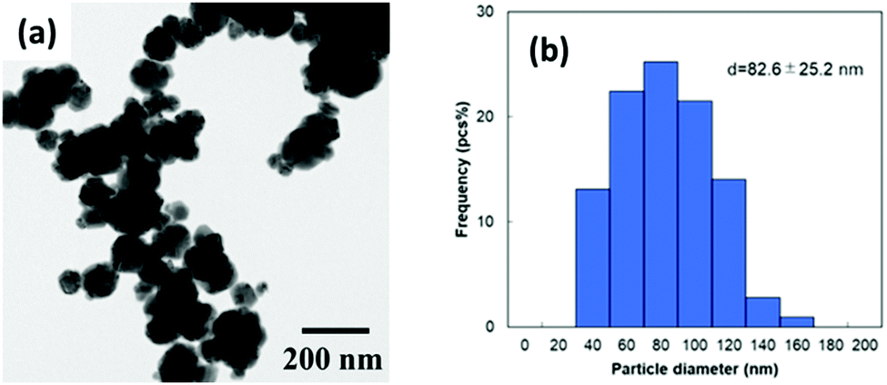 | ||
| Fig. 1 (a) Transmission electron microscopy (TEM) image and (b) size distribution of 1-hexanoic-acid-stabilised copper nanoparticles prepared by hydrazine reduction of CuO micro particles. | ||
 | ||
| Fig. 2 FT-IR spectra of 1-hexanoic acid (orange) and 1-hexanoic acid-stabilised copper nanoparticles (blue) prepared by hydrazine reduction of CuO micro particles. Attribution of the peaks of 1-hexanoic acid: 2976 cm−1, O–H stretch; 1703 cm−1, CO stretch; 1414 cm−1, O–H bend; 1282 cm−1 C–O stretch; and 933 cm−1 O–H bend. | ||
As previously reported, reduction of CuO was completed under these preparation conditions, and no CuO peak could be found in the sample, which indicates that the reduction was complete. The main product of the sample is metallic copper, but a small and broad peak corresponding to Cu-rich orthorhombic copper oxide Cu64O(044) can be observed at 2θ = 40.7°.33 The crystal structure of Cu64O has been reported in the literature.33,35–39
The obtained particles were re-dispersed into DPG by pre-mixing with a planetary centrifuge mixer and milling with zirconia beads (30 μm). The optimised milling conditions found in this study were 1000 rpm for 30 min and 2000 rpm for 30 min.50 When a stronger milling condition was applied (3000 rpm for 30 min), fusion of the particles occurred, forming very large copper flakes. The XRD patterns of the copper particles before milling and in the paste obtained after milling are shown in Fig. 3. After the dispersion milling process, a small and wide cuprous oxide (Cu2O) peak was observed because the milling with beads was carried out under ambient conditions. This small and broad peak corresponding to Cu2O indicates that the surface of the copper nanoparticles was slightly oxidised during milling in air with zirconia beads.
 | ||
| Fig. 3 X-ray diffraction patterns of (yellow) the prepared copper nanoparticles stabilised by 1-hexanoic acid and (blue) the copper nanoparticles after bead milling. The peaks of the solid circle, solid triangle, and solid square correspond to Cu(111), Cu2O(111), and Cu64O(044) planes, respectively. After the milling process, a small and wide peak of Cu2O was observed. | ||
To confirm the detailed crystalline structure of the copper nanoparticles, an aberration-corrected TEM bright-field (BF) image was obtained. Fig. 4 shows the BF image of the copper nanoparticles after milling with zirconia beads. The surface of the particle is covered by an amorphous layer with a thickness of approximately 1.2 nm, which corresponds to the 1-hexanoic acid monolayer and thin amorphous layer of copper oxide. The amorphous formation of copper was probably due to damage during milling with hard zirconia beads. The particles had a hydrophobic surface, which supported the formation of a 1-hexanoic acid monolayer. Crystalline fringe patterns in the metallic cores were carefully observed. Lattice fringes corresponding to metallic Cu(200), Cu-rich copper oxide Cu64O (044), and cuprous oxide Cu2O(111) can be observed in the image. Cu2O is clearly observed on the surface, indicating that the Cu2O layers were generated during milling. The small and broad peak observed in the XRD pattern after milling (Fig. 3(blue)) also suggests that a Cu2O thin layer was generated on the surface of the nanoparticles. Conversely, metallic Cu (200) and Cu64O (044) fringes were found in the core area of the particles. The core of the particles mostly consisted of metallic Cu, and a small portion of Cu64O was found. This result also corresponds to the XRD pattern shown in Fig. 3. From the XRD pattern obtained in this figure, another metaphase such as Cu8O phase cannot be found.
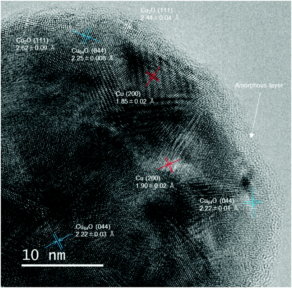 | ||
| Fig. 4 Aberration-corrected TEM bright-field (BF) image of 1-hexanoic-acid-stabilised copper nanoparticles after milling with small zirconia beads (30 μm). (ref. Cu(200) 1.808 Å, Cu64O(044) 2.215 Å, Cu2O(111) 2.465 Å). | ||
X-Ray photospectroscopy (XPS) is well known as a very powerful tool to understand the electronic state of metals and other elements. However, in the case of copper, interpretation of the peaks is quite difficult. No significant difference of binding energies between metallic Cu and Cu2O. Furthermore, in our sample, the layers of Cu64O and Cu2O were found in XRD patterns. It is very difficult to distinguish all three components (Cu, Cu64O and Cu2O) by XPS. Therefore, we have used abbreviation-corrected atomic resolution TEM to reveal the crystalline structures of the surface of copper nanoparticles. Similar discussion was also carried out in the case of gelatine-stabilized copper fine particles.38
In order to understand the stability of 1-hexanoic acid-stabilised copper nanoparticles against temperature, in situ heating XRD measurements were carried out (Fig. 5). The relationship between the temperature and the ratios (w/w) of each component (Cu, Cu64O and Cu2O) obtained by using reference intensity ratio (RIR) method is indicated in Fig. 6. Oxidation of copper surface and increasing of Cu2O peak height can be observed with the temperature increasing. However, up to 80 °C, we can find a small peak corresponding to Cu64O (044) at 2θ of 40.7°. This peak intensity change with temperature strongly supports that the peak here is different from those of metallic Cu, Cu2O and CuO. The weight ratio of Cu64O decreased with the increase of the temperature and over 100 °C, this peak completely disappeared (Fig. 6, green). These changes in the XRD patterns strongly indicate that during heating, mainly metallic Cu was oxidised directly to Cu2O and that Cu64O metaphase is relatively stable even under air.
 | ||
| Fig. 5 In situ heating XRD patterns of 1-hexanoic acid-stabilised copper nanoparticles. The sample was heated under air. | ||
 | ||
| Fig. 6 The weight ratios of Cu (orange left y-axis), Cu2O (red left y-axis), and Cu64O (small green diamonds: left y-axis, green circle: right y-axis) phases in 1-hexanoic acid-stabilised copper nanoparticles. The weight ratios were calculated from the XRD patterns obtained at high temperatures (Fig. 5) using reference intensity ratio (RIR) calculation. | ||
The grain size of the metallic copper in the obtained copper nanoparticles was determined from the Cu (111) peak using Scherrer's equation, as shown in Fig. 2. The grain size of the obtained copper nanoparticles was 14.1 nm, and that of the copper nanoparticles after milling was 15.0 nm. The large difference between the particle diameter and the grain size indicates that these copper nanoparticles have an internal polycrystalline structure. According to Pawlow's thermodynamic model,51,52 the sintering temperature of metal nanoparticles and fine particles depends on the particle size. A smaller grain size is likely to be more useful for low-temperature sintering. The diffusion rate of metal atoms at the grain boundaries is usually higher than that in crystalline cores.
Sintering of printed copper nanoparticle pastes
The obtained copper nanoparticle pastes were printed on alumina substrates and sintered under pure nitrogen gas flow (99.99%) and 3%H2–N2 mixed gas flow. As indicated in Fig. 5 and 6, under air, the copper nanoparticles were oxidised when heated under air. Therefore, for obtaining conductive copper layers, inert or reductive atmosphere is required. Sintering at higher temperatures was beneficial in both cases. Fig. 7 shows digital images of the printed copper paste layers deposited on an alumina substrate using a doctor blade (40 μm) before and after sintering at various temperatures under 3%H2–N2 mixed gas or nitrogen gas. Before sintering, the printed copper layer shows a red-black colour consistent with the plasmon absorption of the copper nanoparticles. Fig. 7(a) and (f) are the digital images of as prepared copper nanoparticle films before sintering. Fig. 7(b)–(e) show digital images of the copper layer sintered under 3%H2–N2 mixed gas. A copper metallic lustre can be observed after sintering, which indicates that sintering was successfully carried out and neckings among the particles were generated. Conversely, as shown in Fig. 7(g)–(j), when the printed layer was sintered under nitrogen flow, no obvious lustre of the copper layer could be found. his is probably due to the fact that fewer necking points were fabricated during sintering under nitrogen flow, as nitrogen is not a reductive gas. In fact, no electrical conductivity was observed when the copper layer was sintered at 120 °C under a nitrogen gas flow, as indicated in Fig. 8. In Fig. S3 (ESI†), RGB (red–green–blue) values of the digital images of the sintered copper layers (Fig. 7) were plotted against the sintering temperatures. The maximum brightness of the digital images was obtained after sintering at 200 °C. The brightness of the layers sintered at 250 °C under nitrogen flow considerably lower than that of the layer sintered at 200 °C. This can be attributed to oxidation of copper particles during sintering without reducing atmosphere as discussed above. | ||
| Fig. 7 Digital images of the surface of the sintered copper nanoparticle layers. (a) Before sintering, (b–e) sintered at various temperatures indicated in the image under 3%H2–N2 gas flow, (f) before sintering, (g–j) sintered at various temperatures under nitrogen gas flow. | ||
 | ||
| Fig. 8 Relationship between the resistivity of the copper layer film after sintering and the sintering temperature. Red: Sintered under nitrogen gas flow. Blue: Sintered under 3%H2–N2 gas flow. | ||
The electrical resistivities of the copper layers sintered between 120 and 250 °C under 3%H2–N2 or nitrogen gas flow are shown in Fig. 8. Surprisingly, our particle layer shows good electrical conductivity after sintering under 3%H2–N2 mixed gas at temperatures as low as 120 °C, which can be used on poly(ethylene terephthalate) (PET) films. The copper layers obtained by sintering under H2–N2 mixed gas flow had a lower resistivity than those sintered under nitrogen gas. Under 3%H2–N2, the lowest resistivity obtained in this study was 5.1 × 10⁻⁶ Ω cm at 250 °C, which is three times that of bulk copper (1.7 × 10⁻⁶ Ω cm). In the previous report, the similar system sintered at 200 °C under 3%H2–N2 gas flow showed the resistivity of 6.63 × 10⁻⁶ Ω cm,50 and it is well corresponding to the results obtained in this study. At temperatures above 160 °C, the value was less than 10−4 Ω cm. It did not reach 10−6 Ω cm level, even after sintering at 250 °C. Because of the lack of reductive conditions, copper oxide layers on the surface of copper nanoparticles prevented necking formation and an increase in conductivity. Reductive conditions are important for generating very low resistivity.
The XRD patterns of the copper layers sintered at various temperatures under 3%H2–N2 and nitrogen gas flow are shown in Fig. 9. (Extra XRD patterns of Cu nanoparticle layers sintered at 140 °C and 180 °C are added in Fig. S4 (ESI†) (3%H2–N2 gas flow) and Fig. S5 (ESI†) (nitrogen gas flow)) Enlarged peaks in the range of 2θ = 30–40° are shown separately in the same figure. The copper layer sintered under a 3%H2–N2 gas flow a show very small peak corresponding to Cu2O up to 150 °C according to the reducing atmosphere. In contrast, in the XRD patterns of the copper layer sintered under nitrogen flow, the peak corresponding to cuprous oxide (Cu2O) became slightly larger after sintering at 150 °C, and this peak is increased with the increase of the sintering temperature. It can be clearly observed in the XRD pattern of the copper layer sintered at 250 °C. This can be attributed to the high sensitivity of metallic copper to a small amount of oxygen in the nitrogen flow (99.99%). However, the peak corresponding to Cu64O(044) could not be found in any of the XRD patterns after sintering. This phenomenon indicates that Cu64O was reduced to metallic copper during sintering in both cases. This reduction with the change in the crystalline structure generates a large diffusion of copper atoms. This diffusion of copper atoms could form neckings between the particles, which enhances the conductivity of the copper layer, even after sintering under nitrogen gas flow. When the paste layer is sintered, the Cu64O layer is reduced to metallic copper by removing oxygen atoms as H2O molecules, and Cu ions are also removed as RCOO–Cu complexes. A detailed discussion is provided below.
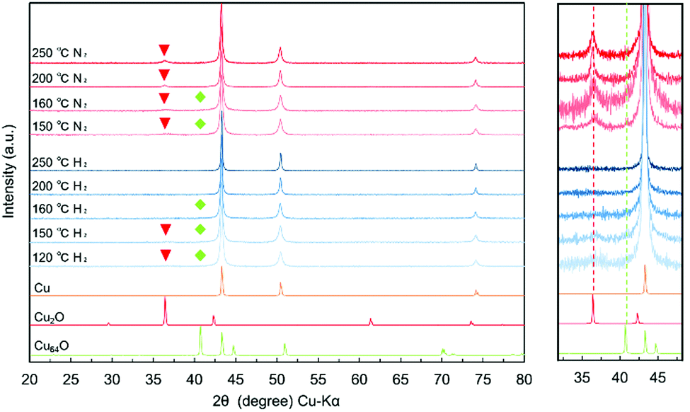 | ||
| Fig. 9 X-ray diffraction patterns of the copper layers sintered at various temperatures under nitrogen gas flow and 3%H2–N2 mixed gas flow. The peak height is normalised to the height of the Cu(111) peak (2θ = 43.3°). Red triangle, red broken line: Cu2O(111) (2θ = 36.4°). Green diamond, green broken line: Cu64O(044) (2θ = 40.7°). | ||
Scanning electron microscopy (SEM) images of the surface morphology of the copper layer after sintering are shown in Fig. 10. These images reveal that the particles form wide necking structures and connect with each other by sintering under a 3%H2–N2 gas flow, even when the particles are fully covered by 1-hexanoic acid molecules. After milling, the copper nanoparticles were slightly oxidised, and Cu2O layers were formed, according to the XRD pattern shown in Fig. 3. Wider necking and network of the particles can be more clearly observed after sintering at higher temperatures (Fig. 10e and g). In contrast, for the copper layers sintered under non-reductive nitrogen gas flow, wide necking structures cannot be found in the SEM images (Fig. 10b, d, f and h), and the particles retained their shape, even at 250 °C. However, after sintering, good conductivity was observed, even after sintering under nitrogen. This suggests that a metallic connection of the particles was formed by the sintering process.
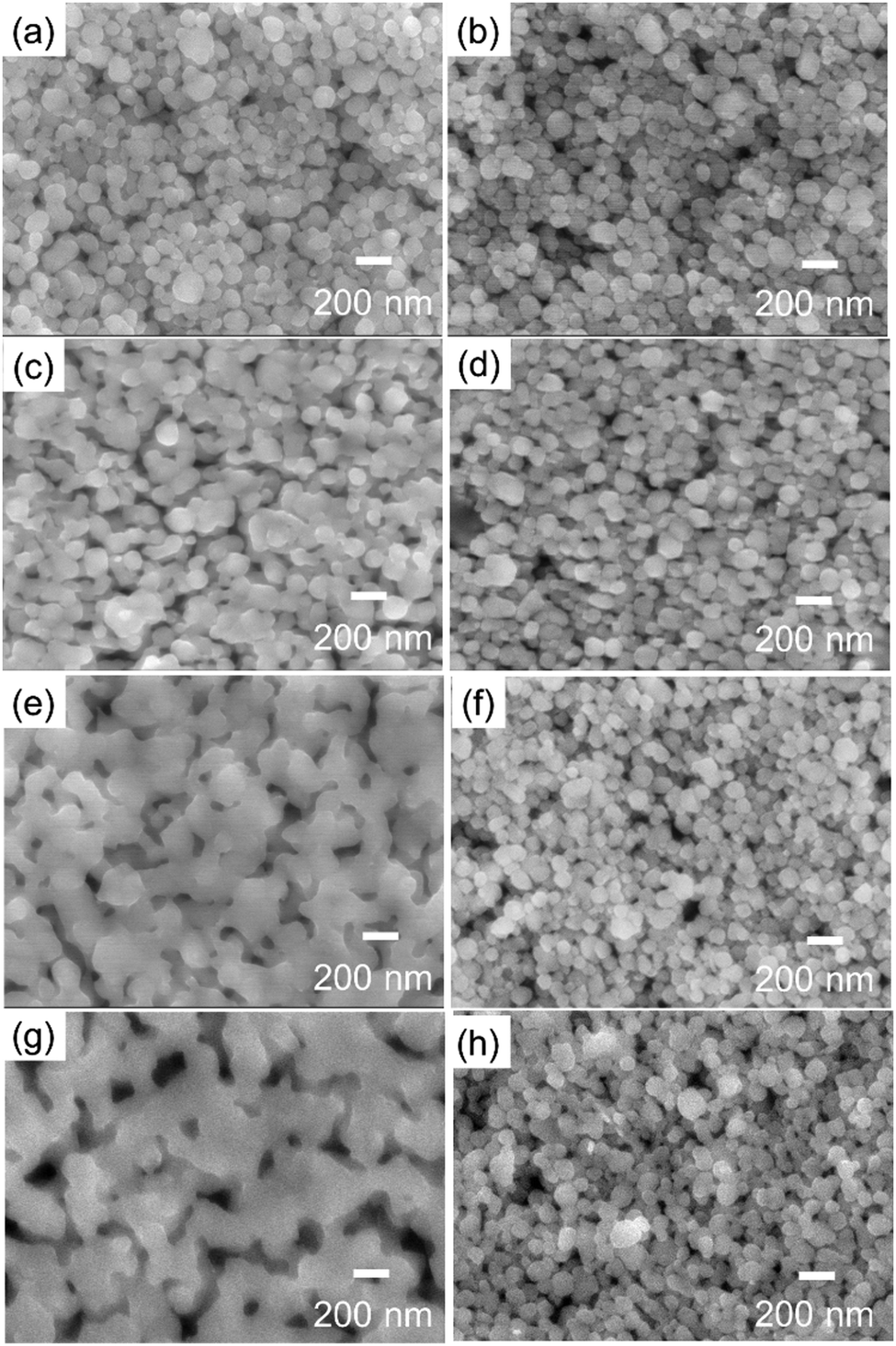 | ||
| Fig. 10 Scanning electron microscopy (SEM) images of the surface of the sintered copper nanoparticles after sintering at various temperatures. (a,c,e,g) Sintered under 3%H2–N2 mixed gas flow, (b,d,f,h) sintered under nitrogen gas flow. Sintering for 1 h at (a and b) 150 °C, (c and d) 180 °C, (e and f) 200 °C, and (g and h) 250 °C. | ||
Cross-section of these sintered Cu nanoparticle layers was also observed by SEM (Fig. S6, ESI†). The particles were densely packed in the sintered layers. The nanoparticles were well sintered especially in the surface region. The layers obtained by sintering under 3%H2–N2 gas flow show the connected surface layers (Fig. S6(e) and (g), ESI†) as indicated also in Fig. 10(e) and (g).
Fig. 11 shows the grain size of the sintered copper layers at various temperatures under a 3%H2–N2 flow and nitrogen flow. The grain sizes were calculated using Scherrer's equation from the Cu(111) peaks shown in Fig. 9, Fig. S4, and S5 (ESI†). In both cases, the grain size of the copper layer after sintering was larger than that of the copper particles. This strongly suggests that copper atom diffusion occurs, even at 140 °C. The grain sizes of the copper layer sintered under 3%H2–N2 flow were larger than those sintered under nitrogen flow. The grain size of the copper layer sintered at 200 °C under 3%H2–N2 flow was almost double that sintered under nitrogen flow. This result indicates that the reduction of Cu2O and Cu64O to metallic copper strongly enhances the very high diffusion coefficient of copper atoms, according to the crystalline structure changes during the reduction.
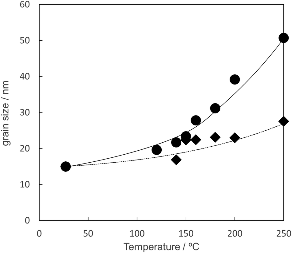 | ||
| Fig. 11 Relationship between the sintering temperature and the grain size of copper in the copper layers. The grain sizes were obtained from Cu(111) peaks of X-ray diffractograms shown in Fig. 9, Fig. S4, and S5 (ESI†) using Scherrer's equation. Closed circle: sintered under 3%H2–N2 gas flow. Closed diamond: sintered under nitrogen gas flow. | ||
The XRD patterns of the sintered copper layers prepared under nitrogen flow (Fig. S5, ESI†) show a broad peak corresponding to Cu2O, but no peak corresponding to Cu64O can be observed. This suggests that the reduction of the surface Cu64O and Cu2O is important for the formation of neckings. Even under a nitrogen atmosphere, the surface copper oxide layer containing Cu64O was removed because of the carboxylic acid group of the stabiliser 1-hexanoic acid. (Fig. 12) The estimated reaction is shown in eqn (1). 1-Hexanoic acid dissolves the oxide layer on the surface of the copper particles under heating. By heating the copper particle layer, metallic copper atoms were generated on the surface, changing the crystal structure. (Cu64O: cuprite structure, Cu: fcc, Fig. 13(a)). During structural deformation, necking between the particles was created to minimise the surface energy. However, at higher temperatures, metallic copper was oxidised to Cu2O by the oxygen molecules included in nitrogen gas (99.99%).
| Cu64O + 2RCOOH → Cu (RCOO)2 + 63Cu + H2O | (1) |
 | ||
| Fig. 12 Schematic illustration of the sintering procedure of 1-hexanoic-acid-stabilised copper nanoparticles with a Cu64O layer. | ||
Moreover, in the presence of hydrogen, the Cu2O layer is reduced to metallic Cu (eqn (2)) more rapidly and form strong neckings between the particles, which results in a lower resistivity than the Cu layer sintered under nitrogen gas flow. The crystalline structure change from Cu2O (cuprite structure) to Cu (fcc).
| Cu2O + H2 → 2Cu + H2O | (2) |
Fig. 13 shows the crystalline structures of the components of the copper nanoparticles and their changes to metallic copper during sintering. The explanation of this structure is introduced in ESI† (Fig. S7,33 S833 and S9, ESI†). Cu64O has an orthorhombic structure, and Cu2O shows a cuprite structure. And metallic Cu has an fcc structure. As the unit cell of Cu64O contains 128 Cu and 2 O atoms, it is very complicated to be instantly understood. Therefore, a crystal with a shape close to that of fcc metallic copper were cut from the Cu64O unit cell (Fig. S9, ESI†) and displayed for easier understanding (Fig. 13(a) left). This cell has two rhombus faces with four rectangle faces.
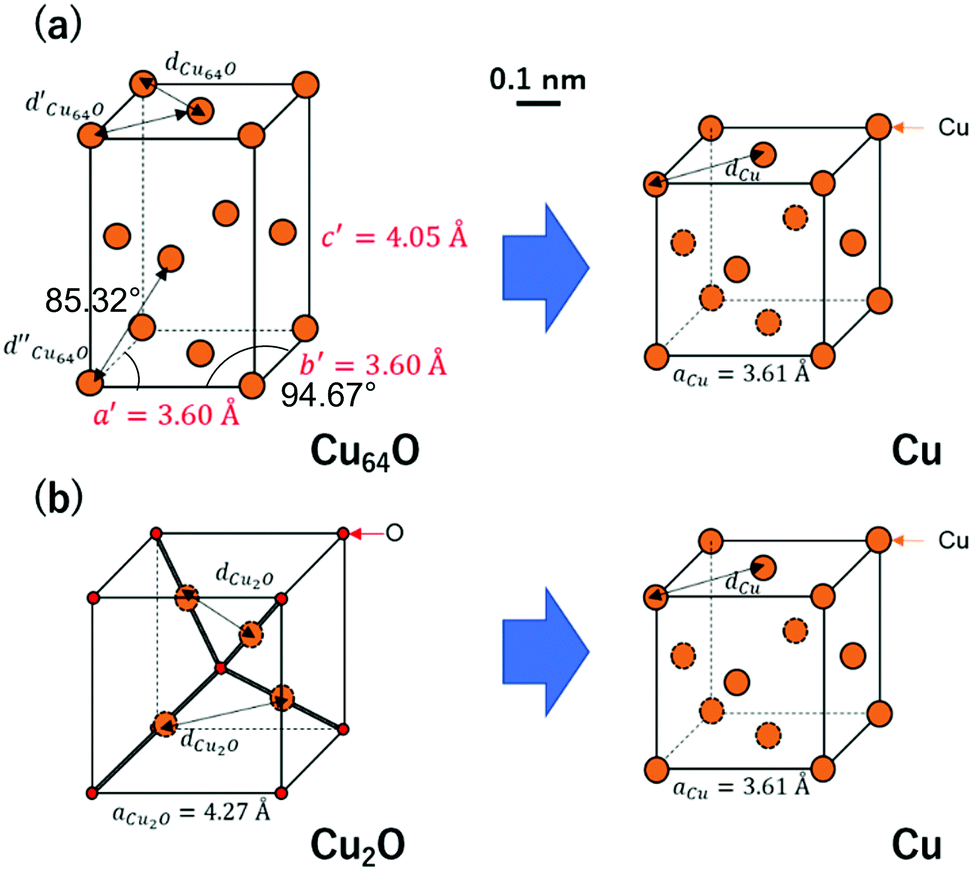 | ||
| Fig. 13 Schematic illustration of crystalline structural changes during sintering. (a) Cu64O to Cu and (b) Cu2O to Cu. | ||
As discussed above, during sintering, 1-hexanoic acid works as a flux and reduces the surface even under nitrogen flow to expose the metallic copper atoms on the surface. The exposed copper atoms connect the nanoparticles for necking. With reduction from Cu64O to metallic Cu (Fig. 13(a)), the length of the c-axis decreased by almost 11%. It can be estimated that this change in the crystal structure from orthorhombic to face-centred cubic leads to a large copper atom diffusion coefficient, even at low temperatures. Conversely, Cu2O can be reduced to metallic Cu during sintering under a 3%H2–N2 flow. In this case, there is a considerable structural change from the cuprite structure to fcc, as shown in Fig. 13(b). This change also introduces a large copper atom diffusion rate.
In the case of silver, Suganuma et al. proposed a similar strategy, “nano-volcanoic” eruption.53 Intermediate Ag–O fluids were generated at the grain boundary of Ag and redeposited on the surface. This mechanism enhances the diffusion of Ag atoms at low temperatures and enables the formation of strong dye bonds and highly conductive films by the low-temperature sintering of silver nanoparticles. However, in the case of copper, the reduction of Cu64O by the flux 1-hexanoic acid and of Cu2O by hydrogen enhances the diffusion of Cu atoms.
To understand the sintering process of 1-hexanoic-acid-stabilised copper nanoparticles, thin samples of the cross-section of the sintered layer were observed by aberration-corrected TEM. The sample for this observation was prepared using a focused ion beam (FIB).
Fig. 14 shows the aberration-corrected TEM results of the cross-sectional thin sample of the copper layer obtained by sintering under a 3%H2–N2 flow at 200 °C. The necking and network of copper particles can be observed in Fig. 14(a). The enlarged image of the necking position (Fig. 14(b)) shows clear lattice fringes corresponding to Cu64O (green numbers). The calculated lattice angles between (404) and (175) and between (036) and (616) of Cu64O were 59.5° and 61.0°, respectively. The angles indicated in Fig. 14(b) correspond well with the calculated values. The lattice fringe corresponding to metallic copper is indicated by the brown numbers. Fig. 14(c) shows the selected area electron diffraction (SAED) pattern of the thin copper layer sample. The spots fit well with metallic copper. The brown numbers indicate the corresponding face numbers of the metallic copper. These TEM observations strongly suggest that the surface of the FIB-sliced samples was slightly oxidised to Cu64O because the samples were exposed to air after FIB treatment, and the core of the sample can be attributed to metallic copper, which suggests that the sintered layer is composed of metallic copper, as indicated by the XRD patterns shown in Fig. 9.
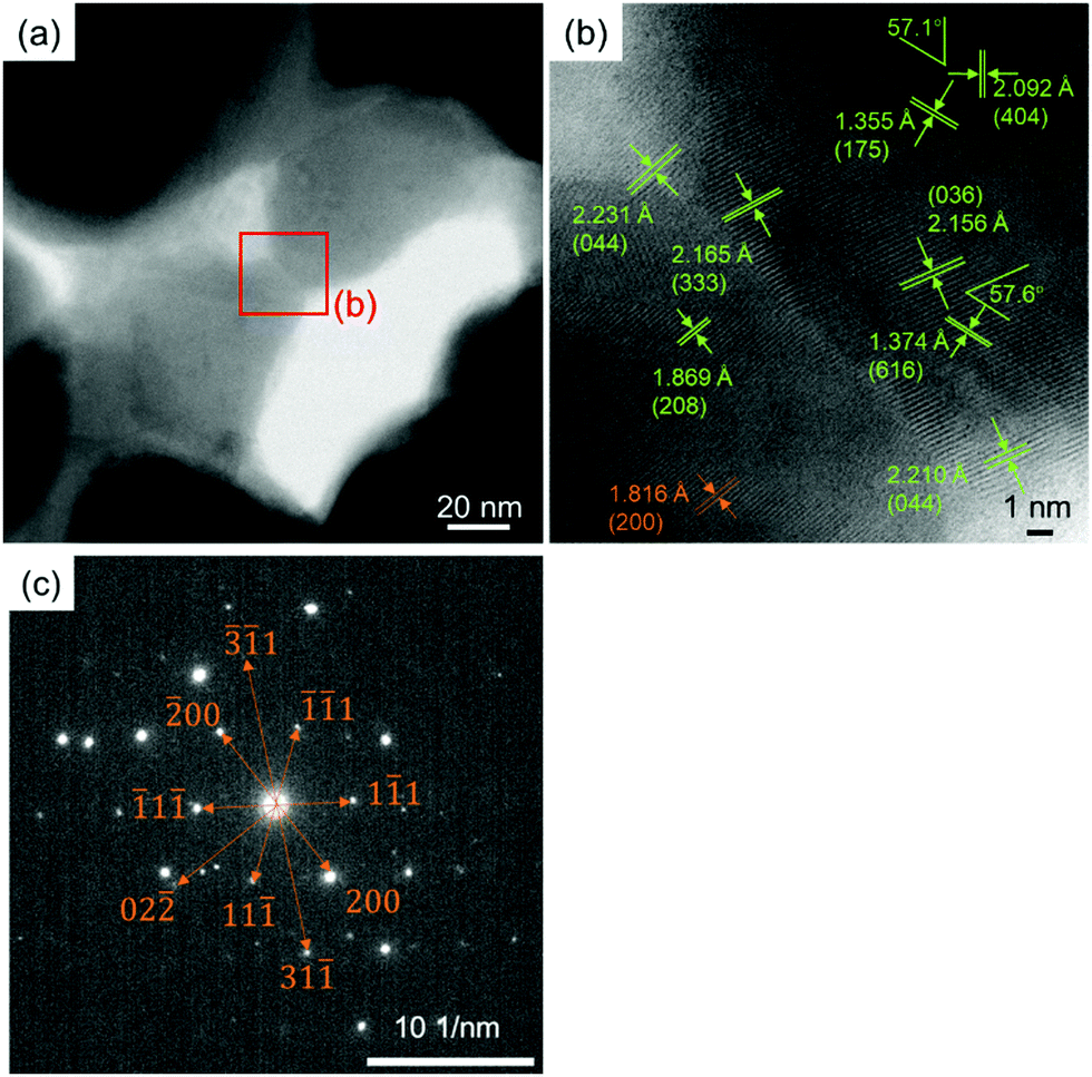 | ||
| Fig. 14 Aberration-corrected TEM images and SAED pattern of the cross-section of the obtained copper layer sintered under 3%H2–N2 flow. The sintering temperature was 200 °C. (b) is an enlarged image of the red square area in (a). Green numbers shown in (b) are the distances of the fringes corresponding to crystalline Cu64O. Brown numbers shown in (c) are the face indexes of the corresponding metallic copper. This indicates that the core of this thin layer is metallic, and the surface is slightly oxidised to Cu64O. The sample was exposed to air after FIB treatment. | ||
Fig. 15 shows the aberration-corrected TEM results of the cross-sectional thin sample of the copper layer obtained by sintering under nitrogen flow at 200 °C. Similar to the copper layer sintered under 3%H2–N2 flow (Fig. 14(a)), neckings and connections of the particles can be observed, as shown in Fig. 15(a). In the enlarged images in Fig. 15(b) and (c), clear lattice fringes can be observed. The calculated lattice angles between (448) and (236) and between (036) and (054) of Cu64O were 50.1° and 77.9°, respectively. The indicated angles in Fig. 15(b) and (c) correspond well with the calculated values. However, unlike the sintering in the 3%H2–N2 flow environment, the sintering in nitrogen flow showed the presence of Cu2O at the edge of neckings, as shown in Fig. 15(b) and (d) (red numbers). This strongly suggests that the necking growth between copper nanoparticles was inhibited by the presence of Cu2O, probably because Cu2O cannot be reduced by 1-hexanoic acid. The existence of Cu2O in the sintered copper layer under nitrogen flow is also indicated by the XRD patterns shown in Fig. S2 (ESI†). From the XRD patterns, the use of hydrogen is highly recommended for the sintering of copper nanoparticles at higher temperatures (>160 °C). Fig. 15(e) shows the selected area electron diffraction (SAED) pattern of the thin copper layer sample, and all spots are attributed to metallic copper (brown numbers). This indicates that the core of the sintered copper layer consisted of metallic copper.
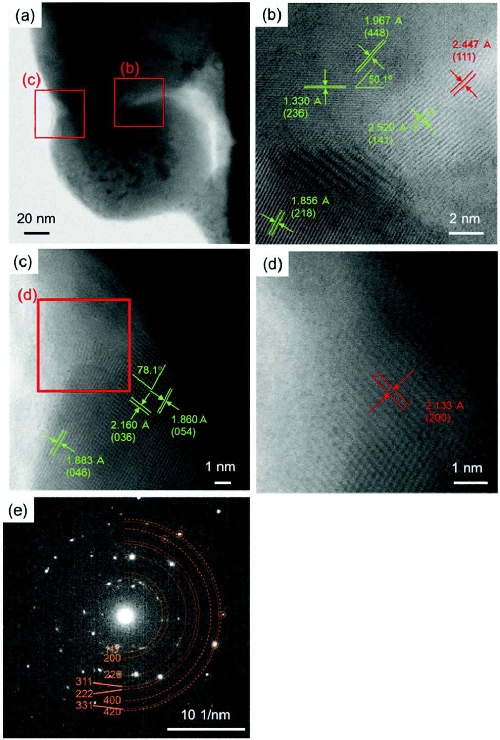 | ||
| Fig. 15 Aberration-corrected TEM images and SAED pattern of the cross-section of the obtained copper layer sintered under nitrogen flow. The sintering temperature was 200 °C. (b) and (c) are enlarged images of the red square area in (a). (d) is an enlarged image of the red square area in (c). Green numbers shown in (b) and (c) are the distances of the fringes and face indexes corresponding to Cu64O crystal. Red numbers shown in (c) and (d) are the distances and face indexes corresponding to crystalline Cu2O. Brown numbers shown in (e) are the face indexes of the corresponding metallic copper. This indicates that the core of this thin layer is metallic, and the surface is slightly oxidised to Cu64O during sample preparation. The sample was exposed to air after FIB treatment. Cu2O was not reduced to copper by sintering under nitrogen. | ||
Fig. 16 is a schematic illustration of necking formation between 1-hexanoic-acid-stabilised copper nanoparticles by low-temperature sintering in a 3%H2–N2 flow and nitrogen flow. To prepare the copper nanoparticle pastes in DPG, the bead milling process was carried out in air. The copper nanoparticles were covered by a very thin Cu2O layer and Cu64O islands, as observed in the high-resolution TEM image of the copper nanoparticles. When the particles were sintered in a 3%H2–N2 flow, all oxides could be reduced to metallic copper and wide neckings were generated as a result of the large copper diffusion coefficient because of the change in crystal structure during reduction. Conversely, when the particles entered the nitrogen flow, Cu64O was successfully reduced by the flux effect of 1-hexanoic acid, generating necking between the particles. However, Cu2O stopped the necking. Therefore, especially at higher temperatures, the grain growth, growth of the necking structure, and network of copper particles after sintering were significantly improved by sintering in the presence of hydrogen, as shown in Fig. 10 and 11, and a higher conductivity was obtained, as indicated in Fig. 8.
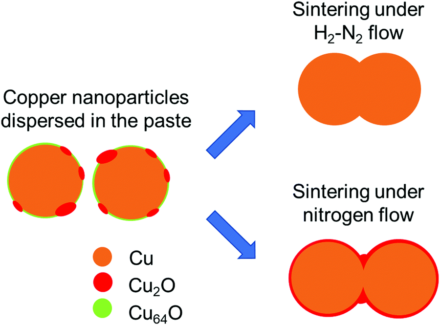 | ||
| Fig. 16 Schematic illustration of necking formation during sintering of 1-hexanoic-acid-stabilised copper nanoparticles. | ||
Conclusions
In the present study, copper nanoparticles stabilised with 1-hexanoic acid were successfully fabricated. Homogeneous copper nanoparticle pastes were obtained using a mill with small bead particles. The obtained paste was printed on an alumina substrate with a doctor blade and sintered under a nitrogen or 3%H2–N2 mixed gas flow. The copper layers obtained after thermal sintering were electrically conductive. The lowest resistivity obtained in this study was 5.1 × 10⁻⁶ Ω cm (250 °C under 3%H2–N2). 1-Hexanoic acid dissolved the Cu64O oxides on the surface of the particles and promoted particle-to-particle bonding. In the sintering under nitrogen, they were bonded in the presence of 1-hexanoic acid, but because of the nitrogen flow, Cu2O was eventually observed at high temperatures.Conflicts of interest
There are no conflicts to declare.Acknowledgements
This work was partially supported by Hokkaido University, a Grant-in-Aid for Challenging Research (Exploratory) (19K22094 to TY), and the Fund for the Promotion of Joint International Research (Fostering Joint International Research (B)) (18KK0159 to TY and MTN) from JSPS, Japan. The authors acknowledge the Adaptable and Seamless Technology transfer Program through targetdriven R&D (A-STEP) funded by the Japan Science and Technology Agency (JST) for the partial financial support. The A3 Foresight Program “Organic/Inorganic Nanohybrid Platforms for Precision Tumour Imaging and Therapy” from JSPS is also gratefully acknowledged. Authors thank Profs T. Satoh and T. Isono (Hokkaido University) for their experimental assistance of FT-IR measurements. It was also partially supported by the Management Expenses Grants for Network Joint Research Centre for Materials and Devices (20211067, 20211242, 20201248, and 20191253). The authors thank Dr Y. Ishida (Hokkaido University) and Prof. T. Sugahara (Osaka University) for fruitful discussions.Notes and references
- W. Wu, Nanoscale, 2017, 9, 7342–7372 RSC.
- A. Kamyshny and S. Magdassi, Chem. Soc. Rev., 2019, 48, 1712–1740 RSC.
- H.-H. Lee, K.-S. Chou and K.-C. Huang, Nanotechnology, 2005, 16, 2436–2441 CrossRef CAS PubMed.
- W. Li, Q. Sun, L. Li, J. Jiu, X.-Y. Liu, M. Kanehara, T. Minari and K. Suganuma, Appl. Mater. Today, 2020, 18, 100451 CrossRef.
- A. C. Arias, J. D. MacKenzie, I. McCulloch, J. Rivnay and A. Salleo, Chem. Rev., 2010, 110, 3–24 CrossRef CAS PubMed.
- M. Mäntysalo and P. Mansikkamäki, AEU Int. J. Electron. Commun., 2009, 63, 31–35 CrossRef.
- M. L. S. N. S. Lakshmi, B. T. P. Madhav, H. Khan and P. V. V. Kishore, Flexible Printed Electron., 2020, 5, 025007 CrossRef CAS.
- J. Kwon, H. Cho, H. Eom, H. Lee, Y. D. Suh, H. Moon, J. Shin, S. Hong and S. H. Ko, ACS Appl. Mater. Chem. Interfaces, 2016, 8, 11575–11582 CrossRef CAS PubMed.
- S. Li, B. N. Peele, C. M. Larson, H. Zhao and R. F. Shepherd, Adv. Mater., 2016, 23, 9770–97750 CrossRef PubMed.
- D. Gao, J. Wang, K. Ai, J. Xiong, S. Li and P. S. Lee, Adv. Intell. Syst., 2020, 2, 2000088 CrossRef.
- P. He, J. Cao, H. Ding, C. Liu, J. Neilson, Z. Li, I. A. Kinloch and B. Derby, ACS Appl. Mater. Interfaces, 2019, 11, 32225–32234 CrossRef CAS PubMed.
- W. Li, H. Zhang, Y. Gao, J. Jiu, C. Li, C. Chen, D. Hu, Y. Goya, Y. Wang, H. Koga, S. Nagao and K. Suganuma, J. Mater. Chem. C, 2017, 5, 1155–1164 RSC.
- T. Yonezawa, S. Takaoka, H. Kishi, K. Ida and M. Tomonari, Nanotechnology, 2008, 19, 145706 CrossRef PubMed.
- Y. Hokita, M. Kanzaki, T. Sugiyama, R. Arakawa and H. Kawasaki, ACS Appl. Mater. Interfaces, 2015, 7, 19382–19389 CrossRef CAS PubMed.
- J. Liu, H. Chen, H. Ji and M. Li, ACS Appl. Mater. Interfaces, 2016, 8, 33289–33298 CrossRef CAS PubMed.
- Y. Zuo, S. Carter-Searjeant, M. Green, L. Mills and S. H. Mannan, Mater. Lett., 2020, 276, 128260 CrossRef CAS.
- J. Xie, J. Shen, J. Deng and X. Chen, J. Electron. Mater., 2020, 49, 2669–2676 CrossRef CAS.
- T. Yonezawa, H. Tsukamoto, Y. Yong, M. T. Nguyen and M. Matsubara, RSC Adv., 2016, 6, 12048–12052 RSC.
- W.-Y. Chung, Y.-C. Lai, T. Yonezawa and Y.-C. Liao, Nanomaterials, 2019, 9, 1071 CrossRef CAS PubMed.
- Y. Yong, M. T. Nguyen, H. Tsukamoto, M. Matsubara, Y.-C. Liao and T. Yonezawa, Sci. Rep., 2017, 7, 45150 CrossRef CAS PubMed.
- P. Calvert, Chem. Mater., 2001, 13, 3299–3305 CrossRef CAS.
- L. Mo, Z. Guo, L. Yang, Q. Zhang, Y. Fang, Z. Xin, Z. Chen, K. Hu, L. Han and L. Li, Mol. Sci., 2019, 20, 2124 CrossRef CAS PubMed.
- L. Mo, Z. Guo, Z. Wang, L. Yang, Y. Fang, Z. Xin, X. Li, Y. Chen, M. Cao, Q. Zhang and L. Li, Nanoscale Res. Lett., 2019, 14, 197 CrossRef PubMed.
- M. Li, Y. Xiao, Z. Zhang and J. Yu, ACS Appl. Mater. Interfaces, 2015, 7, 9157–9168 CrossRef CAS PubMed.
- The Engineering Toolbox webpage. https://www.engineeringtoolbox.com/.
- T. Yonezawa, H. Tsukamoto and M. Matsubara, RSC Adv., 2015, 5, 61290–61297 RSC.
- Y. Yong, M. T. Nguyen, H. Tsukamoto, M. Matsubara, Y.-C. Liao and T. Yonezawa, Sci. Rep., 2017, 7, 45150 CrossRef CAS PubMed.
- W. Li, W. Li, J. Wei, J. Tan and M. Chen, Mater. Chem. Phys., 2014, 146, 82–87 CrossRef CAS.
- R. Tokura and T. Yonezawa, Acc. Mater. Surf. Sci., 2022, 7, 18–26 Search PubMed.
- M. Nishimoto, R. Tokura, M. T. Nguyen and T. Yonezawa, Mater. Trans., 2022 DOI:10.2320/matertrans.MT-N2021004.
- H. Kuwae, K. Yamada, T. Kamibayashi, W. Momose, S. Shoji and J. Mizuno, Trans. Jpn. Inst. Electron. Packag., 2000, 13, E19-014-1–E19-014-9 CrossRef.
- P. Buffat and J. P. Borel, Phys. Rev. A: At., Mol., Opt. Phys., 1976, 13, 2287–2298 CrossRef CAS.
- R. Guan, H. Hashimoto and K. H. Kuo, Acta Crystallogr., Sect. B: Struct. Sci., 1985, 41, 219–225 CrossRef.
- R. Guan, H. Hashimoto and K. H. Kuo, Acta Crystallogr., Sect. B: Struct. Sci., 1984, B40, 560–566 CrossRef CAS.
- A. Kulkami, M. Satbhai, W. Li, D. Bornare, K. Syed and S. Joshi, Mater. Adv., 2022, 3, 418–436 RSC.
- Y. Wu, J. Qiu, H.-K. Kim, Y.-H. Hwang, Y. Wu, Z. Wang, S.-J. Park, H.-K. Kim and Y.-H. Hwang, J. Korean Phys. Soc., 2010, 56, 421–424 CrossRef CAS.
- M. S. Alqahtani, N. M. A. Hadia and S. H. Mohamed, Optik, 2018, 173, 101–109 CrossRef CAS.
- T. Yonezawa, Y. Uchida and H. Tsukamoto, Phys. Chem. Chem. Phys., 2015, 17, 32511–32516 RSC.
- Y. Ahmed, J. Hussain, F. Ullah and S. Asif, engrXiv., 21, Nov. 2020, DOI:10.31224/osf.io/75fa6.
- M. Tomonari, K. Ida, H. Yamashita and T. Yonezawa, J. Nanosci. Nanotechnol., 2008, 8, 2468–2471 CrossRef CAS PubMed.
- T. Yonezawa, H. Tsukamoto and M. T. Nguyen, Adv. Powder Technol., 2017, 28, 1966–1971 CrossRef CAS.
- M. Matsubara, T. Yonezawa and H. Tsukamoto, Bull. Chem. Soc. Jpn., 2015, 88, 1755–1759 CrossRef CAS.
- Y. Kamikoriyama, H. Imamura, A. Muramatsu and K. Kanie, Sci. Rep., 2019, 9, 899 CrossRef PubMed.
- T. Yonezawa, J. Shi, H. Tsukamoto and M. T. Nguyen, MRS Adv., 2019, 4, 413–418 CrossRef CAS.
- Y. Yong, T. Yonezawa, M. Matsubara and H. Tsukamoto, J. Mater. Chem. C, 2015, 3, 5890–5895 RSC.
- S. K. Tam, K. Y. Fung and K. M. Ng, J. Mater. Sci., 2016, 51, 1914–1922 CrossRef CAS.
- K.-M. Huang, H. Tsukamoto, Y. Yong, H.-L. Chiu, M. T. Nguyen, T. Yonezawa and Y.-C. Liao, RSC Adv., 2017, 7, 25095–25110 RSC.
- Y.-R. Jang, C.-H. Ryu, Y.-T. Hwang and H.-S. Kim, Int. J. Precis. Eng., 2021, 8, 471–485 Search PubMed.
- C. C. Leong, L. Lu, J. Y. H. Fuh and Y. S. Wong, Mater. Sci. Eng., A, 2002, 338, 81–88 CrossRef.
- S. Liu, R. Tokura, M. T. Nguyen, H. Tsukamoto and T. Yonezawa, Adv. Powder Technol., 2020, 31, 4570–4575 CrossRef CAS.
- P. Pawlow, Z. Phys. Chem., 1909, 65U, 545–548 CrossRef.
- A. Barybin and V. Shapovalov, J. Appl. Phys., 2011, 109, 034303 CrossRef.
- S.-k. Lin, S. Nagao, E. Yokoi, C. Oh, H. Zhang, Y.-c. Liu, S.-g. Lin and K. Suganuma, Sci. Rep., 2016, 6, 34769 CrossRef CAS PubMed.
Footnote |
| † Electronic supplementary information (ESI) available: Digital images of a water droplet on 1-hexanoic acid-stabilised copper nanoparticles, XRD patterns of copper nanoparticles and CuO precursor powders, RGB values of the digital images of the copper layers sintered at various conditions, XRD patterns of the copper layers sintered at various temperatures and under N2 or 3%H2–N2 atmospheres, cross-sectional SEM images of the sintered copper layers, discussions on the crystal structure of Cu64O. See DOI: https://doi.org/10.1039/d1ma01242h |
| This journal is © The Royal Society of Chemistry 2022 |