
 Open Access Article
 This Open Access Article is licensed under a
 Creative Commons Attribution 3.0 Unported Licence
The electronic stability of tin-halide perovskite charged regions†
Cameron
Underwood
a,
Zhou
Wang
b,
Guosheng
Shao
b,
J. David
Carey
 a and
S. Ravi P.
Silva
*a
a and
S. Ravi P.
Silva
*a
aAdvanced Technology Institute, Department of Electrical & Electronic Engineering, University of Surrey, Guildford, GU2 7XH, UK. E-mail: s.silva@surrey.ac.uk
bState Center for Designer Low-Carbon & Environmental Materials, Zhengzhou University, 100 Kexue Avenue, Zhengzhou 450001, China
First published on 25th January 2022
Abstract
We report on the evolution of the electronic structure and partial oxidation state of tin and iodine in ASnI3, where A = CH3NH3 (MA), CH(NH2)2 (FA) and Cs, with an aim to develop stable, long-term, non-toxic halide-perovskite solar cells. Although charge cannot be directly removed from specific elements, we show a reduction in the charge of primarily SnI3 in a hypothetical [ASnI3]2+ unit cell, which was calculated due to the valence band edge being dominated by Sn 5s and I 5p anti-bonding states, accompanied by a reduction in the unit cell volume of [ASnI3]2+ compared to ASnI3. The band structure calculations show semiconducting behaviour in ASnI3 with metallic behaviour in [ASnI3]2+, and similar behaviour is also found for APbI3 and [APbI3]2+, where the Pb atoms exhibit partial charge compared to Sn. This study allows for the analysis of localised charged regions, directing the contribution of the electronic states to stability in perovskite solar absorbers, such as interface recombination and deep trap states.
Introduction
Hybrid organic–inorganic perovskites (HOIPs) have shown great potential as absorber layers in high-performance photovoltaic (PV) devices with a very low fabrication cost compared to current PV materials.1–4 Furthermore, their power conversion efficiencies (PCEs) have made extremely rapid progress, increasing from 3.8% in 2009 to 25.5%, competing with that of the dominant solar cell material in the market, crystalline silicon (c-Si) at 26.7%, but at a lower predicted cost.5 Most perovskite PVs use lead (Pb) as the metallic component of the absorber layer, which has shown very high performance but has the issue of containing water-soluble toxic lead. Tin (Sn) has emerged as a strong contender for the band gap tuning of perovskites and as a possible replacement for Pb in the perovskite system for toxicity reduction in both 3D and 2D systems.6,7 Sn-based perovskites have shown good promise, with very similar structural parameters and electronic properties, resulting in a band gap closer to the optimum Shockley–Queisser limit requirements. Current progress in Sn-based perovskites is hampered by their instability, resulting in lower PCEs compared to Pb-based perovskites largely due to moisture-induced instability, the presence of deep trap states and degradation.8,9 Instability in air and moisture is inherent with Sn, given that it readily oxidises from its Sn2+ oxidation state, which is needed for the formation of stable perovskite octahedra, to its more energetically stable ionic form of Sn4+, resulting in the decomposition of the perovskite lattice. This is an issue that also affects Pb-based perovskites.10,11 Consequently, Sn-based perovskites are currently extremely susceptible to oxidation in both air and moisture, outstripping the advantage of its non-toxic nature. However, the issue of oxidation affects all perovskite structures, with Sn systems allowing much-needed insight into the instability of perovskites. The main chemical oxidation pathway for Sn-based perovskites has been studied and discussed by Leijtens et al.,10 showing the decomposition of the perovskite lattice in the case of the archetypal CH3NH3SnI3 (MASnI3) via the reaction 2MASnI3 + O2 → 2MAI + SnO2 + SnI4. Deep trap states are the major limiting factor in the device performance of both Pb and Sn perovskite absorbers, trapping photoexcited charge carriers and impeding charge collection. Doherty et al.12 recently showed that hole trap clusters are localised in nanoscale regions in the material, resulting in a distribution of states above the valence band. The modelling of charged perovskite systems may aid in developing future methods for the design of materials that can withstand these distributed states.Significant success in power conversion efficiencies and increased device stability have been shown experimentally in triple cation perovskite combinations,13 where cation A is a combination of CH3NH3 (MA), CH(NH3)2 (FA) and caesium (Cs) but studying mixed cation systems is very challenging computationally, given that the computational cost limits ab initio calculations to unit cells or small supercells in most cases. The simplest alternative is to study the three cases separately. Thus, to understand the effect of a charged region on the structure and electronic properties of Sn-based perovskites, we used ASnI3 and [ASnI3]2+, where A = MA, FA or Cs as the key perovskite structures and employed structural and electronic density functional theory (DFT) calculations and density functional perturbation theory (DFPT) phonon calculations to study the properties of an [ABX3]2+ charged region in the perovskite lattice. We report a novel methodology, which describes a heavily hole-doped unit cell of [ASnI3]2+ as a model system to compare to the neutral ASnI3, using increments of charge between 0 and 2+ to understand the development of the electronic structure as a function of charge. Also, phonon band structures were used to understand the stability in this range of systems. Understanding the properties of charged regions in perovskite solar absorbers allows the investigation of the effect the electronic states on the overall stability of the system and will help develop more resilient perovskite systems to overcome adverse effects such as deep trap states and give long-term stability to electronic structures.
Computational details
The structural and electronic properties of ASnI3 and [MASnI3]2+ were calculated from first principles using non-collinear DFT employing the Perdew–Burke–Ernzerhof (PBE) generalized gradient approximation14 implemented in the Vienna ab initio simulation program (VASP).15–18 Projector augmented-wave PBE pseudopotentials19,20 were used with the addition of spin–orbit coupling (SOC) for density of state and band structure calculations, which cause an underestimation of the band gap relative to experimental values but provide a good qualitative description of the electronic structure of the system. The band gap is improved compared to the calculation without SOC, even though it is further from the experimental value. Wavefunctions were expanded in the plane-wave basis up to an energy cutoff of 700 eV. Total energies were fully relaxed to 10−6 eV and atomic forces were relaxed to 0.01 Å eV−1 using a DFT-D2 van der Waals correction for relaxation calculations.21 A conjugate gradient algorithm was used for ASnI3 calculations and an RMM-DIIS algorithm was used for [ASnI3]2+ given that these structures were shown to relax to the pseudocubic triclinic P1 space group for A = MA, FA and cubic P![[m with combining macron]](https://www.rsc.org/images/entities/i_char_006d_0304.gif) 3m space group for A = Cs, which were lowest in total energy, and these results are shown in Table 1. The calculations were sampled with an 8 × 8 × 8 gamma-centered k-point grid. To force the charge state change in our system from ASnI3 to [ASnI3]2+, the INCAR file in VASP was edited from the default value for number of valence electrons (NELECT), for example from 50 per unit cell to 48 in the case of MASnI3, thus forcing an increase of two positive charges on the system.22 A metastable state was found in each case of [ASnI3]2+ when using a conjugate gradient algorithm (set by IBRION = 2 in VASP), which is higher in energy than the stable state found when using the quasi-Newton RMM-DIIS algorithm (set by IBRION = 1 in VASP), and a comparison of the total energies is shown in Table 2. Also, for locating the neutral structure, Universal Structure Predictor: Evolutionary Xtallography (USPEX)23 was used to attempt to find the lowest energy state of [ASnI3]2+ but resulted in metastable states, as shown in Table 3, which were not ultimately used for pre-relaxation structures given their increased total energy compared to the resultant structure of ASnI3 relaxed with the reduction of two electrons. Therefore, for the subsequent calculations, the charged structure was found by relaxing the structure of ASnI3 with two electrons removed using the quasi-Newton RMM-DIIS algorithm. The resulting band structure and partial density of states (PDOS) were calculated using an initial DFT pre-convergence, PBE energy calculation and PBE band structure calculation using an energy convergence criterion of 10−6 eV and energy cutoff of 700 eV. The band-path takes the path of Γ–M–R–X–Γ–R with a k-point spacing of 100. The band structure and density of states plots were post-processed using sumo.24 Electronic structure calculations were repeated for APbI3 with the band structures shown in the ESI.† For the phonon band structure calculations, the total energies were fully relaxed to 10−12 eV and the atomic forces were relaxed to 10−8 Å eV−1 using a DFT-2 van der Waals correction.21 The phonon band structures were calculated using a 2 × 2 × 2 supercell and 4 × 4 × 4 gamma-centered k-point grid using DFPT25 and plotted using sumo24 and Phonopy26 along the same band path used in the electronic structure calculations. Phonon PDOS calculations were performed using the phonon-pdosplot auxiliary tool in Phonopy. Cs was chosen here to minimise the computational cost, with lower degrees of freedom compared to the organic A sites due to the very high precision calculation needed.
3m space group for A = Cs, which were lowest in total energy, and these results are shown in Table 1. The calculations were sampled with an 8 × 8 × 8 gamma-centered k-point grid. To force the charge state change in our system from ASnI3 to [ASnI3]2+, the INCAR file in VASP was edited from the default value for number of valence electrons (NELECT), for example from 50 per unit cell to 48 in the case of MASnI3, thus forcing an increase of two positive charges on the system.22 A metastable state was found in each case of [ASnI3]2+ when using a conjugate gradient algorithm (set by IBRION = 2 in VASP), which is higher in energy than the stable state found when using the quasi-Newton RMM-DIIS algorithm (set by IBRION = 1 in VASP), and a comparison of the total energies is shown in Table 2. Also, for locating the neutral structure, Universal Structure Predictor: Evolutionary Xtallography (USPEX)23 was used to attempt to find the lowest energy state of [ASnI3]2+ but resulted in metastable states, as shown in Table 3, which were not ultimately used for pre-relaxation structures given their increased total energy compared to the resultant structure of ASnI3 relaxed with the reduction of two electrons. Therefore, for the subsequent calculations, the charged structure was found by relaxing the structure of ASnI3 with two electrons removed using the quasi-Newton RMM-DIIS algorithm. The resulting band structure and partial density of states (PDOS) were calculated using an initial DFT pre-convergence, PBE energy calculation and PBE band structure calculation using an energy convergence criterion of 10−6 eV and energy cutoff of 700 eV. The band-path takes the path of Γ–M–R–X–Γ–R with a k-point spacing of 100. The band structure and density of states plots were post-processed using sumo.24 Electronic structure calculations were repeated for APbI3 with the band structures shown in the ESI.† For the phonon band structure calculations, the total energies were fully relaxed to 10−12 eV and the atomic forces were relaxed to 10−8 Å eV−1 using a DFT-2 van der Waals correction.21 The phonon band structures were calculated using a 2 × 2 × 2 supercell and 4 × 4 × 4 gamma-centered k-point grid using DFPT25 and plotted using sumo24 and Phonopy26 along the same band path used in the electronic structure calculations. Phonon PDOS calculations were performed using the phonon-pdosplot auxiliary tool in Phonopy. Cs was chosen here to minimise the computational cost, with lower degrees of freedom compared to the organic A sites due to the very high precision calculation needed.
| Material | a (Å) | b (Å) | c (Å) | α (θ) | β (θ) | γ (θ) | Unit Cell Volume (Å3) | Total energy per atom (eV) | Total energy (eV) |
|---|---|---|---|---|---|---|---|---|---|
| MASnI3 | 6.18 | 6.25 | 6.28 | 87.11° | 90.85° | 89.25° | 242.60 | 4.37 | 52.40 |
| [MASnI3]2+ | 5.25 | 5.24 | 5.24 | 82.46° | 83.59° | 83.42° | 141.28 | 5.02 | 60.19 |
| Metastable [MASnI3]2+ | 5.74 | 5.78 | 3.83 | 72.86° | 73.03° | 69.84° | 119.59 | 5.19 | 62.22 |
| FASnI3 | 6.34 | 6.29 | 6.31 | 86.81° | 95.90° | 93.51° | 250.26 | 4.74 | 56.83 |
| [FASnI3]2+ | 5.37 | 5.35 | 5.25 | 90.07° | 90.02° | 90.00° | 150.81 | 5.32 | 63.81 |
| Metastable [FASnI3]2+ | 6.76 | 5.23 | 3.55 | 100.32° | 103.55° | 81.02° | 123.00 | 5.43 | 65.11 |
| CsSnI3 | 6.21 | 6.21 | 6.21 | 90.00° | 90.00° | 90.00° | 239.18 | 3.14 | 15.69 |
| [CsSnI3]2+ | 5.15 | 5.15 | 5.15 | 90.00° | 90.00° | 90.00° | 136.74 | 4.86 | 24.32 |
| Metastable [CsSnI3]2+ | 5.93 | 5.74 | 3.21 | 72.63° | 106.81° | 94.08° | 106.91 | 5.16 | 25.82 |
| System | Relaxation algorithm | Resulting structure | Total energy (eV) |
|---|---|---|---|
| CsSnI3 (From cubic input) | Conjugate gradient algorithm | Cubic | 15.26 |
| CsSnI3 (From cubic input) | Quasi-Newton RMM-DIIS | Cubic | 16.89 |
| [CsSnI3]2+ (From cubic input) | Quasi-Newton RMM-DIIS | Cubic | 22.13 |
| [CsSnI3]2+ (From cubic input) | Conjugate gradient algorithm | Triclinic | 25.48 |
| [CsSnI3]2+ (From USPEX input) | Quasi-Newton RMM-DIIS | Tetragonal | 25.82 |
| [CsSnI3]2+ (From USPEX input) | Conjugate gradient algorithm | Tetragonal | 25.83 |
| System | Component | Initial valence electrons | Bader valence charge | Difference |
|---|---|---|---|---|
| MASnI3 | SnI3 Unit | 36 | 35.76 | −0.24 |
| MA | 14 | 14.24 | +0.24 | |
| Total | 50 | 50 | 0 | |
| [MASnI3]2+ | [SnI3]2+ Unit | 34 | 33.75 | −0.25 |
| MA | 14 | 14.25 | +0.25 | |
| Total | 48 | 48 | 0 | |
| FASnI3 | SnI3 Unit | 36 | 35.75 | −0.25 |
| FA | 18 | 18.24 | +0.25 | |
| Total | 54 | 54 | 0 | |
| [FASnI3]2+ | [SnI3]2+ Unit | 34 | 33.79 | −0.20 |
| FA | 18 | 18.19 | +0.20 | |
| Total | 52 | 52 | 0 | |
| CsSnI3 | SnI3 Unit | 36 | 35.86 | −0.14 |
| Cs | 8 | 8.14 | +0.14 | |
| Total | 44 | 44 | 0 | |
| [CsSnI3]2+ | [SnI3]2+ Unit | 34 | 33.84 | −0.16 |
| Cs | 8 | 8.16 | +0.16 | |
| Total | 42 | 42 | 0 |
Results
The relaxed crystal structures of ASnI3 and [ASnI3]2+ are shown in Fig. 1, where A = MA, FA or Cs. [FASnI3]2+ moves towards a pseudocubic orthorhombic geometry with the Pmm2 space group and a decrease in its lattice parameters. [CsSnI3]2+ maintains the cubic P3m space group, but with decreased lattice parameters. All the [ASnI3]2+ structures result in a reduction in the unit cell volume in comparison to their ASnI3 counterparts, which is due to the removal of two valence electrons, as shown in Table S1 (ESI†). This volume reduction was observed in the SnI6 octahedra, with little volume change observed in the A site. Distortion of the SnI6 octahedra was also observed in all cases, with a very significant distortion shown in [MASnI3]2+ and [FASnI3]2+ due to the shape of both molecules as shown in Tables S2–S4, (ESI†) where a rotation of the FA molecule is also shown. In [MASnI3]2+, compared to MASnI3, we observed a reduction in the mean Sn–I bond length by ∼16% from 3.13 Å to 2.65 Å and a change in the I–Sn–I bond angles by up to 14°, whereas only a C–H bond length change of from 1.49 Å to 1.45 Å, a mean C–H bond length change of less than 0.01 Å and a mean N–H bond length reduction from 1.04 Å to 1.03 Å were calculated.
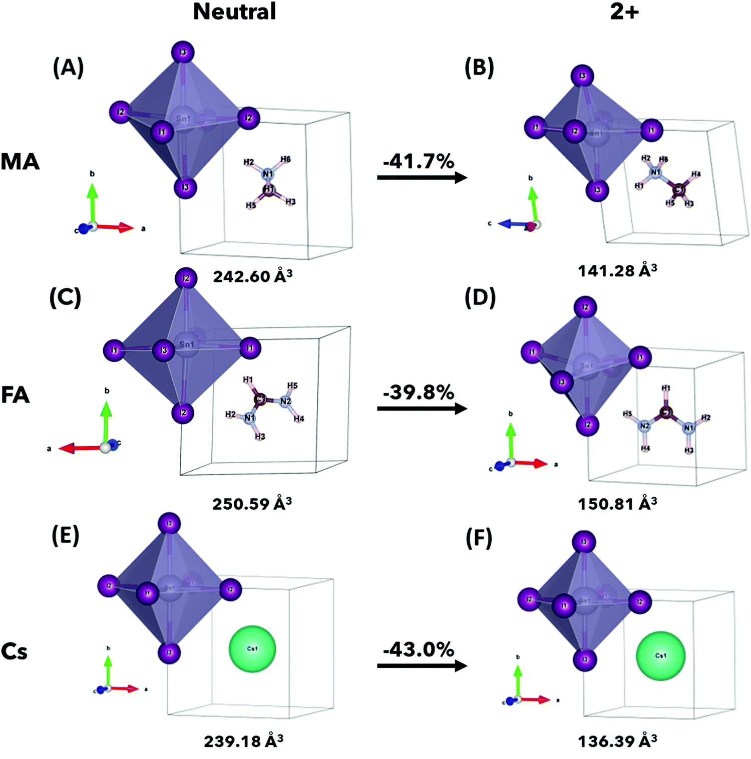 | ||
| Fig. 1 Relaxed unit cells for (A) MASnI3, (B) [MASnI3]2+, (C) FASnI3, (D) [FASnI3]2+, (E) CsSnI3 and (F) [CsSnI3]2+ with labelled atoms (Sn is shown as grey, I as purple, C as brown, N as blue, H as beige and Cs as cyan). Volume relaxation is shown in all cases of [ASnI3]2+ and varying levels of SnI6 octahedral distortion is seen in each case. Volume reduction between ASnI3 and [ASnI3]2+ is indicated by the arrow. | ||
Similar behaviour was observed in [FASnI3]2+ compared to FASnI3, with a mean Sn–I bond length change of ∼18% from 3.31 Å to 2.69 Å and a change in I–Sn–I bond angles of up to 13°, whereas only a mean C–H bond length change from 1.31 Å to 1.29 Å, a C–H bond length change from 1.09 Å to 1.09 Å and a mean N–H bond length change from 1.02 Å to 1.01 Å. An N–C–N bond angle change was also observed from 124.84° to 116.46°. In [CsSnI3]2+ compared to CsSnI3, we observed a mean Sn–I bond length change of ∼14% from 3.10 Å to 2.58 Å, with a very small change in I–Sn–I bond angles of less than 0.01°, which is due to the A+ charge being localized in the center of the unit cell.
It is also worth noting that the magnitude of the total energy of the [ASnI3]2+ relaxed unit cell is significantly higher than that of ASnI3, i.e., 5.02 eV per atom compared to 4.37 eV per atom for A = MA, 5.32 eV per atom compared to 4.74 eV per atom for A = FA and 4.86 eV per atom compared to 3.14 eV per atom for A = Cs. This resultant energy difference is due to the fact that the [ASnI3]2+ system has two electrons removed. This is comparable to the energy of the system plus the partial ionisation energy of Sn and I required to remove the two highest energy valence electrons, where the Sn first ionisation energy is 7.34 eV and the first ionisation energy for I is 10.45 eV.27 Metastable states were also found when using different starting inputs or relaxation algorithms, which were either from a starting point of a cubic unit cell or a starting point of a tetragonal unit cell produced by USPEX, as shown in Table 3 with a visual description of the configuration coordinate energy diagram in Fig. 2. These results can aid in the understanding that the input sensitivity in these strongly doped systems is significant and can result in a variety of local energy minima in the relaxation.
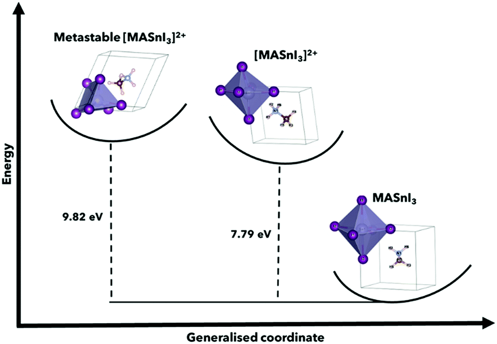 | ||
| Fig. 2 Configuration coordinate energy diagram using MASnI3 and [MASnI3]2+, highlighting the metastable energies for the calculation of perovskite structures, and the variations for A = FA, Cs can be found in Table 1. This shows the found metastable state in comparison to the stable neutral MASnI3 and [MASnI3]2+ systems. The primary driver of the difference in total energy between MASnI3 and [MASnI3]2+ is the reduction in electrons in the unit cell, although this demonstration allows us to understand the relative energy of the metastable state suggested by USPEX compared to the lower energy [MASnI3]2+ structure. | ||
Bader charge analysis28–30 was used to analyse the charge density of our system and calculate the associated charge to each ion. The initial valence electrons for each atom/ion is shown in Table S1, (ESI†) where these are the initial charges in our ab initio calculations, before the energy minimisation calculation. Once the structure was relaxed, each ion in the resulting charge density plot was assigned a value of valence charge by the Bader charge analysis. The summary of this Bader charge analysis for ASnI3 and [ASnI3]2+ is shown in Tables S5–S7, (ESI†) where atoms are as labelled as in Fig. 1. The Bader charge analysis shows that the two-electron reduction was found primarily in the SnI3 unit compared to the A site, as summarised in Table 3.
The SnI3 unit shows an approximate decrease of two in electron charge, shared between Sn and I (this is shown in more detail in Tables S5–S7, ESI†). This is related to the Sn 5s and the I 5p states, which occupy the highest energies in the valence band, given that these are the first to be removed. It was noted that the charge deficiency in the system is shared by Sn and I in the SnI3 unit. This makes the Sn cations less donating and I anions more accepting of electronic charge, thus giving rise to an elevation in the valence band maximum, typical for p-type materials, where this phenomenon is consistent with typical ionic compounds such as doped TiO2.31 This results in the distortion of the octahedra in our relaxed [MASnI3]2+ and [FASnI3]2+ unit cells, whereas the MA and FA molecules remain essentially the same (the small difference here likely originates from the ionic bond between the A and the SnI3 unit being slightly closer in the [ASnI3]2+ cases). We also note that the Bader charge for the H atoms bonded to N is lower than that of the other H atoms, which is due to the hydrogen bonding with I atoms in the octahedra. The results for APbI3 and [APbI3]2+ are shown in Tables S9–S11, (ESI†) where Pb shows a reduced decrease compared to Sn, which is due to the lower energy of the Pb 6s states relative to Sn 5s, where Pb 6s = −11.6 eV and Sn 5s = −10.1 eV under vacuum.32
The resulting band structures for ASnI3 and [ASnI3]2+ are shown in Fig. 3. MASnI3 shows a band gap of 0.179 eV in Fig. 3(A), and we observed the indirect band gap to be 7 meV below the direct band gap transition due to Rashba splitting, which is attributed to the reduced inversion symmetry of the system, as also shown in the study by Wang et al. (2017) in the case of MAPbI3.33 We noted that the band gaps were underestimated due to the choice of the PBE functional with SOC, but this has been shown to generate accurate electronic properties and band characteristics. We repeated the band structure calculation using a k-point mesh of 4 × 4 × 4 and the HSE06 hybrid functional, without spin orbit coupling and calculated a band gap of 1.36 eV for MASnI3, which is very close to the experimentally measured band gap of 1.30 eV,34 as shown in Fig. S4 (ESI†). We calculated a band gap of 0.113 eV for FASnI3, as shown in Fig. 3(C), and 0.060 eV for CsSnI3, as shown in Fig. 3(E). A metallic band structure was observed for all cases of [ASnI3]2+ with the occupancy shown at the Fermi energy. The original bands occupying the previous VBM and CBM were observed at around 2 eV in all cases, which were calculated for the case of an entirely charged material and suggest a tenancy towards p-type semiconducting behaviour in the bulk material of smaller charge. Specifically, as the valence band is pushed up with respect to the Fermi energy, as shown in Fig. 4, where a transition is shown for incremental charges between 0 and 2, this illustrates the transition towards the 2+ structures used in this research, where the results are easier to observe and give a comparison for a more material realistic situation of lower hole doping. Given that the band gap is underestimated via the use of PBE, we can follow this trend to indicate an overall trend towards conductivity, rather than an explicit quantity of charge reduction needed to cause metallic behavior. This is because the band structures here will show conductivity at a lower quantity of charge reduction shown, as the original band gap is reduced. As shown by the Bader charge analysis, most of the states removed are associated with the top of the valence band, where in this case, mostly I 5p and some Sn 5s states. In [ASnI3]2+, due to its strained unit cell, we also observed a broadening in the population of the other states besides the Sn 5s, Sn 5p and I 5p shown to originally be most prevalent in ASnI3. This shows the change in band structure characteristics after the partial oxidation of Sn and I and is shown in more detail compared to the MA composition shown in Fig. S1 (ESI†). This is comparable to the experimental data given that it has been reported that the influence of Sn4+ on the MASnI3 system results in metal-like conductivity.35,36 Our calculations describe behaviour comparable to these [ASnI3]2+ regions within the ASnI3 material, which can be generalised to understand the behaviour of Pb- and Ge-based perovskites, which maintain a similar electronic structure, as shown in the ESI† for Pb.
 | ||
| Fig. 3 Band structure and density of states plots for (A) MASnI3, (B) [MASnI3]2+, (C) FASnI3, (D) [FASnI3]2+, (E) CsSnI3 and (F) [CsSnI3]2+, where the orbital projections highlighting Sn s, Sn p and I p are shown on the band structure plot according to the key in the top left of each plot, and the partial density of state projections for Sn and I are shown in the key in the top right of each plot. All energies are relative to the Fermi energy (EF). | ||
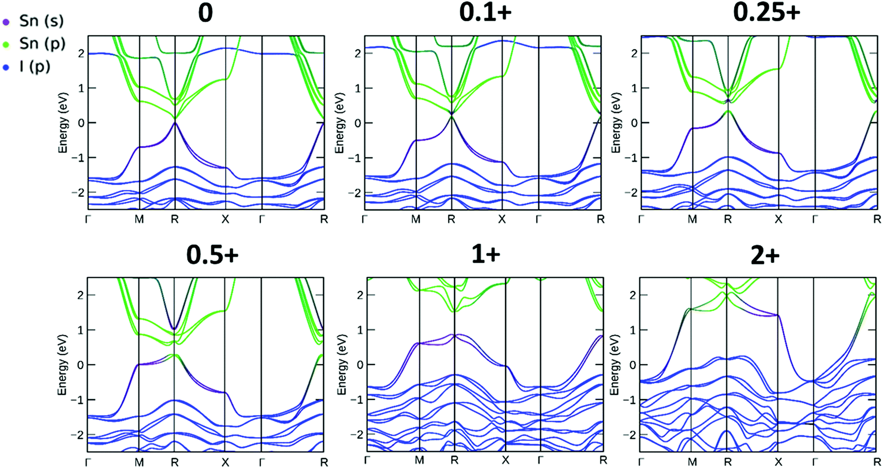 | ||
| Fig. 4 Band structure for increasing total charge between FASnI3 and [FASnI3]2+. A transition from semiconducting to p-doping to metallic behaviour is observed with increasing charge. All energies are relative to the Fermi energy (EF). | ||
The stability of the resulting structure was analysed with use of the calculated phonon band structure. The phonon band structure for CsSnI3 and [CsSnI3]2+ is shown in Fig. 5(A and B), respectively. Negative frequencies were calculated for CsSnI3, which can be used to infer the dynamic instability in the cubic phase of CsSnI3 at 0 K, which is consistent with theory and shown at the R and Γ specific points.37,38 These negative frequencies have been shown to been quenched for cubic CsSnI3 by 500 K.39 The larger negative frequencies calculated for [CsSnI3]2+ can be used to infer significant instability and are also shown at the Γ specific point, which increases the significance of the inferred structural instabilities and is due to the distorted resulting system. The phonon partial density of states was calculated for CsSnI3 and [CsSnI3]2+ and shown in Fig. 5(C and D), respectively. In [CsSnI3]2+, the soft modes and majority of the density of states are contributed by Sn and I, which overlap at low frequencies, and Cs is less affected but shows some soft modes compared to the case of CsSnI3, where the frequency range is narrower and the negative frequency modes are dominated by I. Due to the increase in the range of frequencies, the PDOS is broader in general in the case of [CsSnI3]2+, where the maximum height of the peaks is an order of magnitude less than that of CsSnI3. This increase in frequency range is due to the decreased lattice parameter and resultant structural instability, which is due to the lack of electrons in the Sn–I3 octahedra. Similar results are shown for CsPbI3 and [CsPbI3]2+ in Fig. S5 and S6, (ESI†) respectively, with the majority of negative modes in [CsPbI3]2+ being comprised of I and Sn, which is a reflection of the reduction in electrons shown primarily in I and Sn in Table S11, (ESI†) as well as following the same properties of CsSnI3, also showing negative modes associated with I.
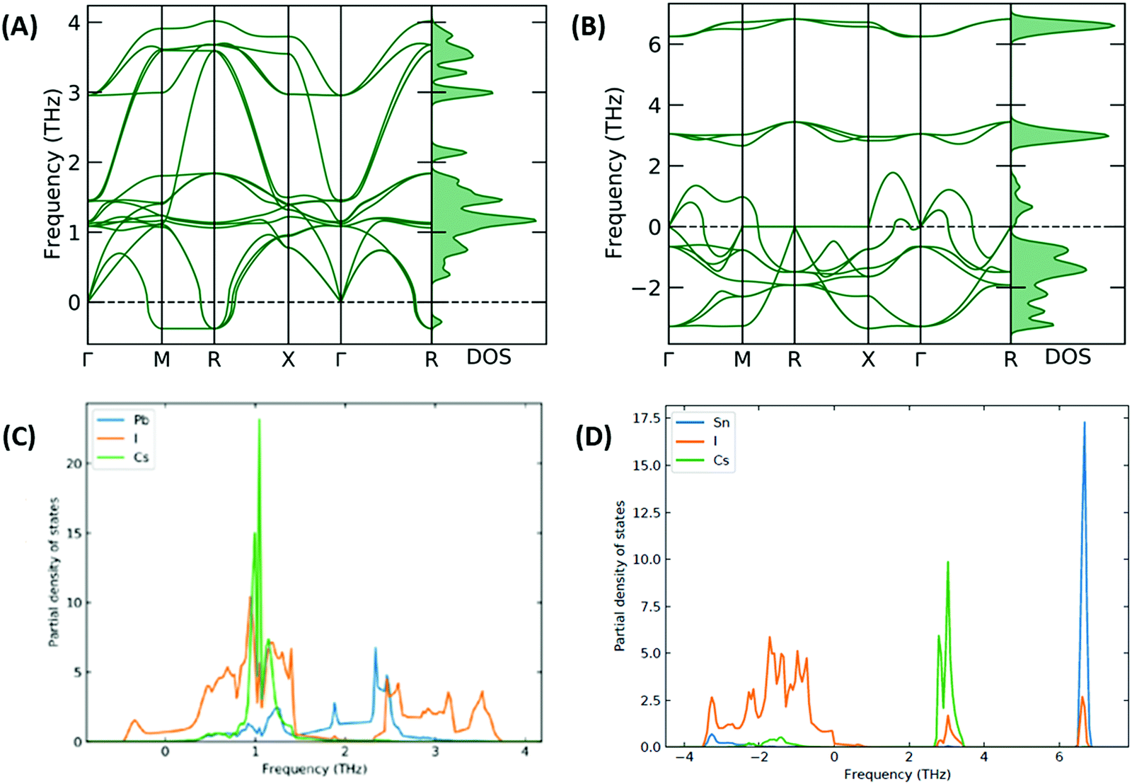 | ||
| Fig. 5 Phonon band structure and density of states for (A) CsSnI3 and (B) [CsSnI3]2+ as well as phonon partial density of states for (C) CsSnI3 and (D) [CsSnI3]2+. Larger negative frequencies are shown in the case of [CsSnI3]2+, indicating dynamic instability, which are associated primarily with the reduction in electrons, primarily in Sn and I, as shown via the highest energy states in the electronic partial density of states, and described by the Bader charge analysis. | ||
Conclusion
An investigation into charged organometallic tin-halide perovskite absorber systems was undertaken to model the effect of a charged region on a fixed perovskite structure, and long-term stability based on electronic charge was analysed. A DFT PBE structural analysis was made and the effect of removing two electrons from the system was discussed. The appearance of calculated metastable states was shown, where this energy landscape may cause instabilities in the material in the presence of overall charge. We performed PBE band structure calculations for both ASnI3 and [ASnI3]2+, where A = MA, FA and Cs, which provided a comprehensive study of the three components of the triple cation system currently in use. The electronic band structures calculated for ASnI3 with a lack of inversion symmetry have indirect band gap behaviour due to Rashba splitting or a direct band gap when inversion symmetry is held, which is consistent with the semiconducting properties experimentally observed for this material. The electronic band structures calculated for [ASnI3]2+ show metallic behaviour in all cases, with the VBM pushed above the position of the Fermi energy, which is comparable with the instability of the solar cell performance observed experimentally in tin-halide perovskite solar cells. The phonon band structure calculated for CsSnI3 shows more structural stability, whereas [CsSnI3]2+ shows significant instability due to the presence of large negative frequency modes. This is caused by the resultant strain due to the change in the size of the Sn–I3 octahedra as a result of the loss of electrostatic charge in the octahedra. Therefore, instabilities were shown here in Sn and I due to the charged state of the system, whereas thermal stabilities have been previously shown due to the movement of Cs in the triple cation metal halide perovskites. This analysis aims to pave the way for the analysis of other charged perovskite 3D and 2D structures and deep charge trap states in perovskite solar absorbers with a view to solve the longer-term stability issues in Pb-free perovskites.Abbreviations
| DFT | Density functional theory. |
| VASP | Vienna Ab Initio Simulation Package. |
| PBE | Perdew–Burke–Ernzerhof |
| DOS | Density of states. |
| PDOS | Partial density of states |
| PV | Photovoltaic |
| PCE | Power conversion efficiency |
Author contributions
The manuscript was written through contributions of all authors.Funding sources
This work was funded and supported by the Engineering and Physical Sciences Research Council (EPSRC) Grant Number GR/1922310/1 and the European Union's Horizon 2020 Musicode No. 953187 EU Horizon Project.Conflicts of interest
There are no conflicts to declare.References
- G. Kojima, K. Teshima, Y. Shirai and T. Miyasaka, Organometal halide perovskites as visible-light sensitizers for photovoltaic cells, J. Am. Chem. Soc., 2009, 131(17), 6050–6051 CrossRef PubMed.
- J. Burschka, N. Pellet, S. J. Moon, R. Humphry-Baker, P. Gao, M. K. Nazeeruddin and M. Grätzel, Sequential deposition as a route to high-performance perovskite-sensitized solar cells, Nature, 2013, 499(7458), 316–319 CrossRef CAS PubMed.
- M. A. Green, A. Ho-Baillie and H. J. Snaith, The emergence of perovskite solar cells, Nat. Photonics, 2014, 8(7), 506 CrossRef CAS.
- M. Liu, M. B. Johnston and H. J. Snaith, Efficient planar heterojunction perovskite solar cells by vapour deposition, Nature, 2013, 501(7467), 395–398 CrossRef CAS PubMed.
- NREL, Best Research-Cell Efficiencies (Accessed 15/12/2020).
- C. C. Underwood, J. D. Carey and S. R. P. Silva, Nonlinear Band Gap Dependence of Mixed Pb–Sn 2D Ruddlesden–Popper PEA2Pb1−xSnxI4 Perovskites, J. Phys. Chem. Lett., 2021, 12(5), 1501–1506 CrossRef CAS PubMed.
- C. C. Underwood, J. D. Carey and S. R. P. Silva, Influence of A site cation on nonlinear band gap dependence of 2D Ruddlesden–Popper A2Pb1−xSnxI4 perovskites, Mater. Adv., 2021, 2(15), 5254–5261 RSC.
- W. Ke and M. G. Kanatzidis, Prospects for low-toxicity lead-free perovskite solar cells, Nat. Commun., 2019, 10, 965 CrossRef PubMed.
- H. Yao, F. Zhou, Z. Li, Z. Ci, L. Ding and Z. Jin, Strategies for Improving the Stability of Tin-Based Perovskite (ASnX3) Solar Cells, Adv. Sci., 2020, 7(10), 1903540 CrossRef CAS PubMed.
- T. Leijtens, R. Prasanna, A. Gold-Parker, M. F. Toney and M. D. McGehee, Mechanism of tin oxidation and stabilization by lead substitution in tin halide perovskites, ACS Energy Lett., 2017, 2(9), 2159–2165 CrossRef CAS.
- N. K. Noel, S. D. Stranks, A. Abate, C. Wehrenfennig, S. Guarnera, A. A. Haghighirad, A. Sadhanala, G. E. Eperon, S. K. Pathak, M. B. Johnston and A. Petrozza, Lead-free organic–inorganic tin halide perovskites for photovoltaic applications, Energy Environ. Sci., 2014, 7(9), 3061–3068 RSC.
- T. A. Doherty, A. J. Winchester, S. Macpherson, D. N. Johnstone, V. Pareek, E. M. Tennyson, S. Kosar, F. U. Kosasih, M. Anaya, M. Abdi-Jalebi, Z. Andaji-Garmaroudi, E. L. Wong, J. Madéo, Y. Chiang, J. Park, Y. Jung, C. E. Peroukhoff, G. Divitini, M. K. L. Man, C. Ducati, A. Walsh, P. A. Midgley, K. M. Dani and S. D. Stranks, Performance-limiting nanoscale trap clusters at grain junctions in halide perovskites, Nature, 2020, 580(7803), 360–366 CrossRef CAS PubMed.
- B. Conings, J. Drijkoningen, J. Gauquelin, A. Babayigit, J. D’Haen, L. D’Olieslaeger, A. Ethirajan, J. Verbeeck, J. Manca, E. Mosconi and F. D. Angelis, Intrinsic thermal instability of methylammonium lead trihalide perovskite, Adv. Energy Mater., 2015, 5(15), 1500477 CrossRef.
- J. P. Perdew, K. Burke and M. Ernzerhof, Generalized gradient approximation made simple, Phys. Rev. Lett., 1996, 77(18), 3865 CrossRef CAS PubMed.
- G. Kresse and J. Hafner, Ab initio molecular dynamics for liquid metals, Phys. Rev. B: Condens. Matter Mater. Phys., 1993, 47(1), 558 CrossRef CAS PubMed.
- G. Kresse and J. Hafner, Ab initio molecular-dynamics simulation of the liquid-metal- amorphous-semiconductor transition in germanium, Rev. B: Condens. Matter Mater. Phys., 1994, 49, 14251 CrossRef CAS PubMed.
- G. Kresse and J. Furthmüller, Efficiency of Ab-initio total energy calculations for metals and semiconductors using a plane-wave basis set, Comput. Mater. Sci., 1996, 6(1), 15–50 CrossRef CAS.
- G. Kresse and J. Furthmüller, Efficient iterative schemes for ab initio total-energy calcu- lations using a plane-wave basis set, Comput. Mater. Sci., 1996, 54(16), 11169 CAS.
- G. Kresse and D. Joubert, From ultrasoft pseudopotentials to the projector augmented- wave method, Rev. B: Condens. Matter Mater. Phys., 1999, 59, 1758 CrossRef CAS.
- P. E. Blöchl, Projector augmented-wave method, Rev. B: Condens. Matter Mater. Phys., 1994, 50(24), 17953 CrossRef PubMed.
- S. Grimme, Semiempirical GGA-type density functional constructed with a long-range dispersion correction, J. Comput. Chem., 2006, 27(15), 1787–1799 CrossRef CAS PubMed.
- G. Kresse and J. Furthmüller, “VASP the GUIDE”. (Computational Materials Physics, Faculty of Physics, Universitat Wien, 2016 Search PubMed.
- C. W. Glass, A. R. Oganov and N. Hansen, USPEX – evolutionary crystal structure prediction, Comput. Phys. Commun., 2006, 175, 713–720 CrossRef CAS.
- A. Ganose, A. Jackson and D. Scanlon, sumo: Command-line tools for plotting and analysis of periodic Ab initio calculations, J. Open Source Softw., 2018, 3(28), 717 CrossRef.
- S. Baroni, S. De Gironcoli, A. Dal Corso and P. Giannozzi, Phonons and related crystal properties from density-functional perturbation theory, Rev. Mod. Phys., 2001, 73(2), 515 CrossRef CAS.
- A. Togo and I. Tanaka, First principles phonon calculations in materials science, Scr. Mater., 2015, 107, 1–5 CrossRef.
- D. R. Lide, CRC Handbook, CRC Handbook of Chemistry and Physics, CRC Press, 88th edn, 2007 Search PubMed.
- G. Henkelman, A. Arnaldsson and H. Jónsson, A fast and robust algorithm for Bader decomposition of charge density, Comput. Mater. Sci., 2006, 36(3), 354–360 CrossRef.
- E. Sanville, S. D. Kenny, R. Smith and G. Henkelman, Improved grid-based algorithm for Bader charge allocation, J. Comput. Chem., 2007, 28(5), 899–908 CrossRef CAS PubMed.
- W. Tang, E. Sanville and G. Henkelman, A grid-based Bader analysis algorithm without lattice bias, J. Phys.: Condens. Matter, 2009, 21(8), 084204 CrossRef CAS PubMed.
- T. Umebayashi, T. Yamaki, H. Itoh and K. Asai, Band gap narrowing of titanium dioxide by sulfur doping, Appl. Phys. Lett., 2002, 81(3), 454–456 CrossRef CAS.
- J. Qian, B. Xu and W. Tian, A comprehensive theoretical study of halide perovskites ABX3, Org. Electron., 2016, 37, 61–73 CrossRef CAS.
- T. Wang, B. Daiber, J. M. Frost, S. A. Mann, E. C. Garnett, A. Walsh and B. Ehrler, Indirect to direct bandgap transition in methylammonium lead halide perovskite, Energy Environ. Sci., 2017, 10(2), 509–515 RSC.
- R. M. I. Bandara, K. D. G. I. Jayawardena, S. O. Adeyemo, S. J. Hinder, J. A. Smith, H. M. Thirimanne, N. C. Wong, F. M. Amin, B. G. Freestone, A. J. Parnell, D. G. Lidzey, H. J. Joyce, R. A. Sporea and S. R. P. Silva, Tin (iv) dopant removal through anti-solvent engineering enabling tin based perovskite solar cells with high charge carrier mobilities, J. Mater. Chem. C, 2019, 7, 8389–8397 RSC.
- H. S. Jung and N. Park, Perovskite solar cells: from materials to devices, Small, 2015, 11(1), 10–25 CrossRef CAS PubMed.
- Y. Zong, Z. Zhou, M. Chen, N. P. Padture and Y. Zhou, Lewis-Adduct Mediated Grain-Boundary Functionalization for Efficient Ideal-Bandgap Perovskite Solar Cells with Superior Stability, Adv. Energy Mater., 2018, 8(27), 1800997 CrossRef.
- C. E. Patrick, K. W. Jacobsen and K. S. Thygesen, Anharmonic stabilization and band gap renormalization in the perovskite CsSnI3, Rev. B: Condens. Matter Mater. Phys., 2015, 92(20), 201205 CrossRef.
- A. Marronnier, H. Lee, B. Geffroy, J. Even, Y. Bonnassieux and G. Roma, Structural instabilities related to highly anharmonic phonons in halide perovskites, J. Phys. Chem. Lett., 2017, 8(12), 2659–2665 CrossRef CAS PubMed.
- C. E. Patrick, K. W. Jacobsen and K. S. Thygesen, Anharmonic stabilization and band gap renormalization in the perovskite CsSnI3, Rev. B: Condens. Matter Mater. Phys., 2015, 92(20), 201205 CrossRef.
Footnote |
| † Electronic supplementary information (ESI) available: Supplementary information is available containing structural information, A site PDOS and detailed Bader charge data as well as relaxed structure files; this also contains information on APbI3. See DOI: 10.1039/d1ma01232k |
| This journal is © The Royal Society of Chemistry 2022 |