DOI:
10.1039/D1MA01096D
(Paper)
Mater. Adv., 2022,
3, 2089-2095
Enhanced photosensitive properties of a single-crystal formamidinium lead bromide iodine (FAPbBr2I) based photodetector†
Received
19th November 2021
, Accepted 3rd January 2022
First published on 6th January 2022
Abstract
In this work, the growth of formamidinium (FA) based mixed halide perovskite single-crystals using the inverse temperature crystallization method is investigated and characterized to detect their photosensitive properties. The structural characterization of the as-grown single crystals was studied using X-ray diffractometry to confirm whether they belong to the {110} family of planes with a high crystallinity. Their optical properties were studied using UV-Vis spectroscopy, which showed a band-gap of 2 eV, and photoluminescence (PL) spectroscopy. The formation of the Ag/FAPbBr2I/Ag structure was tested under an applied bias voltage of up to ±5 V using different excitation light sources. The results showed a remarkable photosensitive performance with a peak current of 1 μA with corresponding responsivity and detectivity values of 0.8 A W−1 and 1.81 × 10¹¹ Jones, respectively, under exposure to a visible (376 nm) laser.
1 Introduction
Perovskite solar cells were discovered in 2009, and since then those based on organic and inorganic metal halides have attracted significant attention.1 Owing to their advanced optoelectronic properties, such as a high carrier mobility, broadband light absorption, and long carrier diffusion length, perovskite materials based on organic–inorganic lead halide have recently attracted remarkable interest.2 Their extraordinary material characteristics have prompted the revolution of a wide range of highly efficient, flexible, and low-cost optoelectronic and photovoltaic devices.3 Methylammonium lead iodide (MAPbI3) is one of the most common, well-known, and effective perovskite materials for solar cell applications, as well as for single-crystal growth. It has been reported that if the halide atom is changed to I, Br, and Cl, the perovskite material band-gap progressively varies, for example, MAPbI3 (1.38 eV), MAPbBr3 (2.17 eV), and MAPbCl3 (2.84 eV).4,5 Along with the mixed halide (Cl and Br), perovskite (MAPbClxBrx−3) single crystals have also been intensively studied.6 Unfortunately, the methylammonium (MA) molecule has a low thermal stability that is responsible for the degradation of the perovskite material, resulting in a risk to the long-term stability of the device.7 Hence, to develop a highly stable device, the best method is to use a MA-free perovskite material. Recently, FA-based perovskite materials have attracted significant attention owing to their photovoltaic performance that is comparable to that of the MA-based perovskites.8 Moreover, it has been observed that the replacement of the MA cation by the FA cation results in a more stable perovskite structure with an increased solar cell power conversion efficiency.9 The advantage of the FA ions over the MA ions is that the FA ions possess a greater size, and owing to this, they form a more systematic perovskite structure and hence contribute to superior stabilities in the FA-based perovskite.10 In addition to the solar cells, the FA-based perovskite single crystals (PSCs) are also desirable owing to their unique optical and electrical properties that make them attractive for use in optoelectronic devices, such as light-emitting diodes and photodetectors.11,12 A single-crystal grown by using retrograde solubility for halide (Br and I) FA-based perovskite (FAPbBr3, FAPbI3) materials has already been reported.10 Owing to the recent development in technologies, micromorphologies, and the compositions of perovskite materials, research on highly efficient photodetector devices based on different hybrid perovskite materials (organic–inorganic) has become a very attractive area.13 In the field of optical communication and night vision, photodetectors have been used for various applications. They have also been used to develop biosensors and in video imaging.14 The photodetectors made of perovskite are classified into photodiodes and photoconductors according to the different device structures.15,16 The fabrication of photoconductors is easy compared to that of photodiodes. However, photoconductors suffer from a slow response and high voltage requirements. The photodiodes also possess a higher extraction efficiency owing to the presence of hole and electron transport layers.17
Herein, we report the fabrication of a FA-perovskite single crystal-based photodetector. This work mainly focuses on the growth of mixed halide single-crystals and compares the optical properties of the as-grown halide perovskite single crystal with that of the mixed halide PSCs. All of the PSCs were grown as a single-crystal by using the anti-solvent assisted method, which increases the growth rate and can result in the growth of crystals within an hour.18 The fabricated photodetector device exhibits an excellent photoresponse, for example, an approximate enhancement of an order of magnitude for the responsivity (0.8 A W−1), and detectivity (1.81 × 10¹¹ Jones) for a visible (376 nm) laser. A proportional investigation of the FA-based perovskite single-crystals with a mixed halide atom was performed involving optical analysis using UV-visible (UV-Vis) and photoluminescence (PL) spectroscopy and structural analysis using X-ray diffraction (XRD) measurements.
2 Materials
PbI2 (lead iodide), PbBr2 (lead bromide), FAI (formamidinium iodide), and FABr (formamidinium iodide), as well as dimethylformamide (DMF) as a solvent, were purchased from Sigma-Aldrich. These chemicals were used without any further purification.
3 Synthesis of the perovskite single-crystals
All of the perovskite single-crystals were successfully grown by utilizing the inverse temperature crystallization (ITC) technique. In the ITC technique, the selection of the solvent is one of the most important steps as the solvent can lose its solubility if the temperature of the solution is increased, thus providing retrograde solubility. Generally, upon increasing the temperature of the precursor solution, the solute dissolves, and this results in a higher insolubility. In the case of retrograde solubility, the solubility rate decreases, which is key to crystallization. This occurs with a specific salt and is suitable for a particular solvent.
The ITC method is appropriate for the low-temperature growth of PSCs. In the ITC method, the excess PbI2 complex changes into Pb2+ ions to assist the nucleation at a low temperature. In addition, the antisolvent in the precursor (liquid or vapor form) will result in the poor solubility of the precursor solutions. Previously reported literature suggests that the γ-butyrolactone (GBL) solvent is suitable for iodine halogen atom perovskites, in which acetonitrile (ACN) will act as an antisolvent, and DMF, as well as dimethlysulfoxide (DMSO), are suitable solvents for the bromine atom perovskite, in which formic acid (FAH) acts as an antisolvent.19–21 The FA-based perovskite is highly suitable for growing a single-crystal using the ITC method, and retrograde solubility enables the facile and rapid growth of the PSCs. Here, an iodine-based single-crystal is grown by selecting GBL as a solvent. Thereafter, a 1 M solution in the optimum solvent GBL is prepared and stirred at 45 °C. After some time, a clear solution is obtained. When the solution is transparent, an antisolvent is added by filtering it through a polytetrafluoroethylene (PTFE) filter with a pore size of 45 μm in diameter. By filtering, undesirable nucleation is avoided, and hence this does not affect the single-crystal growth. Finally, the structure of the perovskite is shown in Fig. 1c. The process for growing PSCs with different halide ions is explained below.
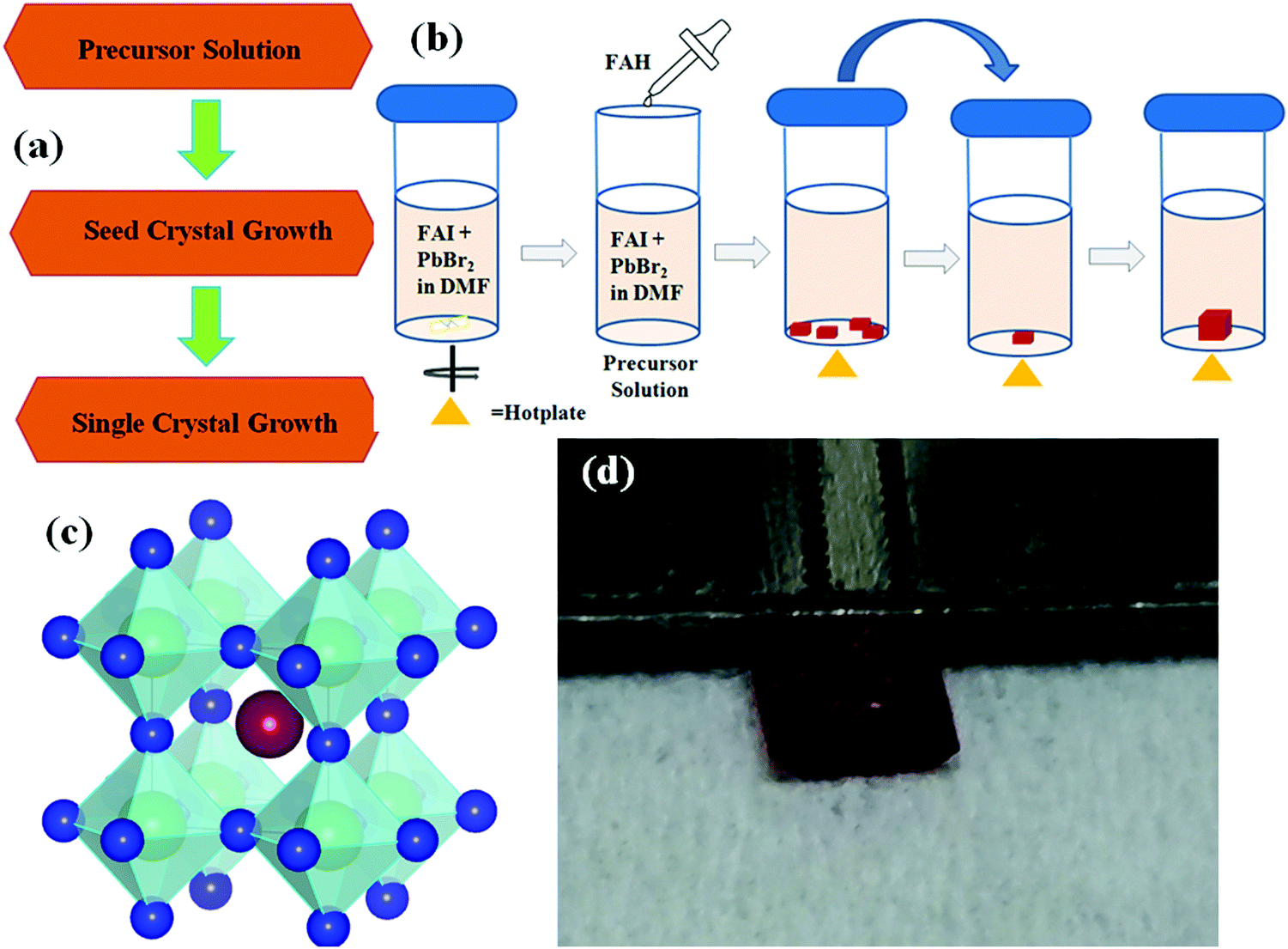
 |
| | Fig. 1 (a) Flow chart showing the synthesis of a single-crystal, (b) schematic representation of the growth of a perovskite single-crystal, (c) perovskite structure and (d) image showing a FAPbBr2I perovskite single crystal. | |
3.1 Preparation of the mixed halide perovskite (FAPbBr2I) single-crystal in DMF
Fig. 1a shows a flow chart of the process used to grow a complete single crystal. It includes the growth of seed crystals by making precursor solutions. In order to grow larger-sized crystals, the seed crystals were put into a separate new solution. For preparing FAPbBr2I, DMF is used as a solvent as it is highly suitable for retrograde solubility. Fig. 1b shows the step-by-step perovskite single crystal growth method. First, the bromide mixed salts (FAI + PbBr2) are prepared by taking a 1 M solution in DMF and this is called the precursor solution. The precursor solution is stirred at room temperature until it turns into a clear solution. Thereafter, FAH is added to the precursor solution. Finally, the solution is filtered using PTFE, kept in a vial and called the mother solution. A vial containing the mother solution is kept in a silicon oil bath at 65 °C. The tiny shimmering single crystal grows in the bottom of the vial. In the next step, one of the shiny seed crystal is picked up and placed into fresh mother solution and kept it in a silicon oil bath at 65 °C. Similarly, both the FAPbI3 and FAPbBr3 PSCs were also grown using the ITC method.22 Thus, the FA-based mixed halide (FAPbBr2I), along with the FAPbI3 and FAPbBr3 perovskite single crystals, were successfully grown via the ITC technique.
4 Discussion
4.1 Photophysical properties of the FA-based perovskite single crystals
For the optical characterization studies, the photoluminescence (PL), as well as the absorption properties, have been studied. To probe the recombination behavior and charge transfer efficiency, the PL characteristics of the FAPbBr2I perovskite single crystal-synthesized via ITC have been studied. The PL spectrum of the as-grown FAPbBr2I perovskite single-crystal was studied at a fixed excitation wavelength at room temperature within the 560–740 nm wavelength range, as shown in Fig. 2a. The broad luminescence peaks were observed around 611 and 660 nm (approximately), and this wavelength corresponds to the band-gap energy. By examining the energy, it seems that the peak around 611 nm corresponds to either the interband or excitonic transition. The 611 nm peak disappears immediately if the sample contains some impurities, and in that case, only one peak corresponding to 660 nm is obtained. The peak that appears at 660 nm is considered to be a result of the defect levels, or impurities that exist in the sample. Alternatively, luminescence peaks generated by the cooled sample corresponds to excitons that start resolving below 600 nm, and the reason for this is the suppression of the thermal broadening of the peak. Measurement of the UV-Vis absorbance of the synthesized FAPbBr2I perovskite single-crystal was performed to probe the interactions (electronic) inside the crystal. Fig. 2b illustrates the absorption spectra of the FAPbBr2I perovskite single-crystal at room temperature in the wavelength range of 500–850 nm. A band-gap of approximately 2.0 eV is observed (Fig. 2b) for the FAPbBr2I perovskite single crystal. This band-gap corresponds to a single absorption peak obtained in the UV analysis. The mixed halide PSCs absorption edge and photoluminescence emission peak are in good agreement with each other, and they also match the results of the optical characterization of the reported thin-film perovskite.23 The higher spectral density suggests that the prepared single crystals are highly crystalline in nature, which were subsequently determined to be low in the case of the polycrystalline perovskite films.24–26 The resultant band gap depicts the influence of the halide ions present during the growing process on the optical properties of the crystal.
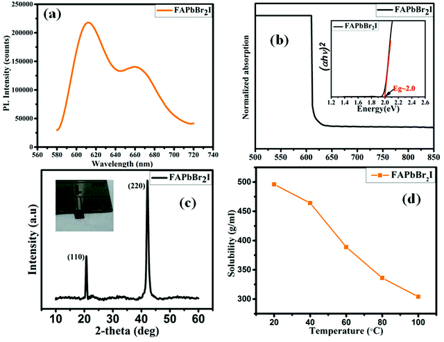 |
| | Fig. 2 (a and b) Emission spectra and absorption spectra for the formamidinium mixed halide (inset Tauc plot). (c) XRD pattern and inset crystal image of the formamidinium FAPbBr2I perovskite single-crystals. (d) Shows the solubility test performances of the perovskite single-crystals. | |
4.2 Structural properties of the FA-based perovskite single crystals
The XRD spectroscopy analysis was performed after the production of the FAPbBr2I single-crystal. Fig. 2c depicts the XRD graph of the perovskite (FAPbBr2I) single-crystal. Prominent XRD peaks were obtained at 2θ–20.7° and approximately 42.1°, denoted by the planes (110) and (220), respectively. These planes show a high crystallinity and were confirmed using the XRD pattern, which revealed a single-crystal that elongated along the direction of the {110} unit. The inset in Fig. 2c shows the image of the FAPbBr2I single-crystal.
4.3 Top-view of the FA-based perovskite single crystal
The scanning electron microscopy (SEM) image of the prepared single-crystal is shown in Fig. S5 in the ESI.† The image reveals the rough surface of the as-grown single-crystal, however, the surface is not smooth. This may be a result of potential fluctuation in the kinetic growth mechanism that hinders these ions from attaching to nearby ions, thus preventing the growth of a uniform profile.
4.4 Solubility test performance of the FA-based perovskite single crystal
To perform a solubility test for the perovskite FA-based single-crystal in their respective solution, a FAPbBr2I single-crystal was ground using a mortar and pestle to form a fine powder. A small amount of the FAPbBr2I powder (0.01 g) was added to the solvent. The solution was stirred and heated to form a clear solution. An equal amount of the solute was added after every 30 min and the solution was tested at different temperatures. It was observed that the solubility decreased with an increase in the temperature, as shown in Fig. 2d. The above process performed in the temperature range of 20–100 °C within the same solution and this was used to conduct the solubility test.
4.5 Photocurrent analysis study using different types of lasers irradiated FAPbBr2I single crystals
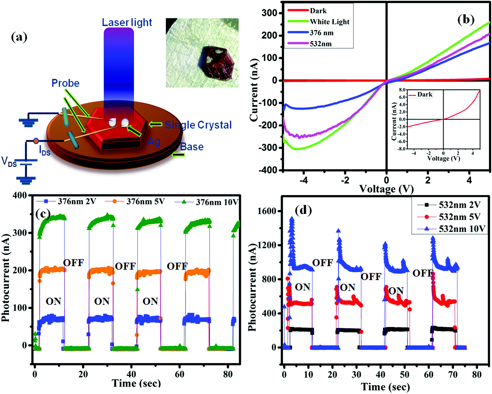
The conversion of a photon into electricity in the devices, the I–V curve, changes under different types of illumination irradiated on the sample. Thus, the I–V characteristics were investigated by making a Ag (silver) contact (ESI,† S1) with the perovskite single crystal. Fig. 3b showed the I–V (current–voltage) characteristics of the fabricated device under different illumination sources. It was observed that the photocurrent increases rapidly when irradiated with a white light and the power response value reaches a few hundred nA, in contrast the current response in the dark was in single digits. Fig. 3a shows the probe station carrying a single-crystal of FAPbBr2I for the I–V characterization. The light on/off current response was successfully tested, as shown in Fig. 3c and d, which depicts the very high repeatability with different voltage values, demonstrating that the photodetector device possesses a good optical switching behavior. In Fig. 3c, it was clearly observed that a sharp increase in the photocurrent arises with the increase in the bias voltage (2, 5 and 10 V) at an incident photon wavelength of 376 nm. This is because the carrier drift velocity speeds up at a high bias voltage, and the photoelectric current was amplified in a very short period of time by several orders of magnitude. Similar results were obtained when the incident laser beam has a wavelength of 532 nm with different bias voltages (2, 5, and 10 V) as shown in Fig. 3d. Furthermore, to measure the time response performance of the FAPbBr2I single crystal-based photodetector devices, the curves of the photoresponse (dependent on time) were calculated under two different types of laser, 376 and 532 nm, illuminated using light with an intensity of 32 mW cm−2 at different bias voltages. It can be observed from Fig. 3c and d that both the photodetector devices based on the FAPbBr2I single-crystal maintained steady response speeds and photocurrent values, indicating that the photodetector devices possess a good stability and reversibility.27,28 The current increases quickly after turning on the light, and there is a sharp fall in the current observed when the light intensity is reduced, which reveals that the surface of perovskite film provides the capacitive response for the different states.29,30
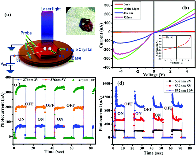 |
| | Fig. 3 (a) Illustration of the probe station, the inset shows the crystal image ready to be characterized, and (b) I–V characteristics of the FAPbBr2I single-crystal. (c) Rise in the photocurrent and the decay characteristics of the bias voltage with an ON/OFF 376 nm laser incident on the FAPbBr2I single-crystal. (d) Rise in the photocurrent and decay characteristics of the bias voltage with an ON/OFF 532 nm laser incident on the FAPbBr2I single crystal. | |
4.6 Time-dependent photocurrent response of the FAPbBr2I perovskite single crystal
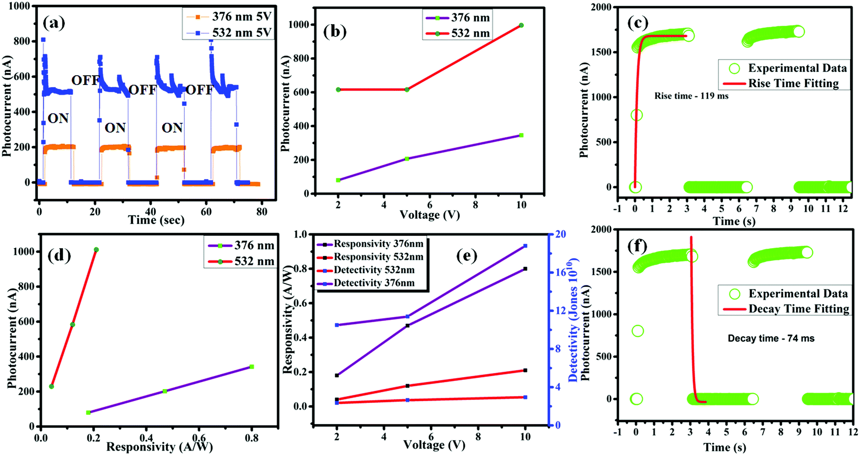
Perovskite single-crystal-based photodetector devices have been reported recently and a few of these are mentioned in Table 1. The reported data comprises the photodetector devices based on FAPbI3, MAPbI2.5Br0.5, MAPbIxBr3−x, MAPbCl3, and with different materials used for carrier transport.14,31–34 In this work, for the purposes of comparison, the amount of responsivity and the detectivity of the photodetector devices based on the FAPbBr2I single-crystal sample are shown in Table 1. It can be clearly observed that the responsivity and detectivity of the photodetector devices based on the FAPbBr2I single-crystal sample are higher than most of the previously reported photodetector devices and also comparable with the highest results reported for the photosensitive materials that form the photodetector devices. The outstanding performance of the photodetector devices based on the FAPbBr2I single-crystal sample are generally a result of the improved photocurrent collection performance and efficiency of the carrier transport. The time dependent photoresponse curves, with an “ON/OFF” state under illumination at 376 and 532 nm at different five bias voltages, were measured and are shown in Fig. 4a, furthermore, the photosensitivity under white light is shown in the ESI,† S3. At a light intensity of 32 mW cm−2 at five different bias voltages, the switching ratio of the photodetector device based on the FAPbBr2I single-crystal sample was very high. The phenomenon resulted in a high switching ratio and indicates that the photodetector device has a high photosensitivity.14 Despite all of these advantages, the photodiodes suffer from a typical switching ratio that reduces their application in comparison to the photoconductors. It is important to mention that the switching ratio is a result of the low intensity of light and this problem can be resolved in the future. A photocurrent of approximately 1 μA was achieved by using a wavelength of 532 nm at a bias voltage of 10 V under a power illumination of 32 mW cm−2 (Fig. 4b). Furthermore, through the analysis shown in Fig. 4c, the time taken for the photocurrent rise after the photodetector device based on the sample was triggered and it was about 119 ms. Fig. 4f clearly shows that the decay time is 74 ms after the irradiation has ended. Fig. 4d depicts the graph between the photocurrent (nA) and the responsivity (A W−1). It can be observed that the photocurrent increases abruptly at a laser wavelength of 532 nm, but a slight variation was observed for 376 nm and the extended photocurrent response is shown in the ESI,† S2. Nonetheless, the high variation in the responsivity for the 376 nm light source is directly related to the fact that higher the energy of the photon, the higher the responsivity will be. Fig. 4e shows the dependence of the calculated responsivity on the voltage, showing the responsivity of the FAPbBr2I photodetector increases with an increase in the voltage. Moreover, to determine the sensibility of detecting a weak optical signal, the detectivity was measured and calculated. The detectivity was calculated to be 1.8 × 10¹¹ Jones at a luminescent light intensity of 32 mW cm−2 at 376 nm and a bias voltage of 10 V. These results are superior or comparable to the previously reported photodetectors shown in Table 1. The values for the responsivity and detectivity for different voltages (2, 5 and 10 V) at two different excitation sources, that is 376 and 532 nm, were calculated and are detailed in Table 2. It was observed that the responsivity and detectivity reach maximum values under a visible laser (376 nm) corresponding to 10 V.
Table 1 Single-crystalline mixed halide perovskite-based detectors and their photocurrent properties
|
|
Perovskite-based detector |
Responsivity |
Detectivity |
Rise time |
Fall time |
Ref. |
| (i) |
FAPbI3 |
0.68 A W−1 |
— |
12.4 ms |
17.2 ms |
31
|
| (ii) |
MAPbI2.5Br0.5 |
∼0.1 A W−1 |
∼4 × 10¹² |
<10 μs |
<10 μs |
32
|
| (iii) |
MAPbIxBr3−x |
∼0.01 A W−1 |
— |
2.3 s |
2.7 s |
33
|
| (iv) |
MAPbCl3 |
∼0.05 A W−1 |
1.2 × 10¹⁰ |
24 ms |
62 ms |
34
|
| (v) |
FAPbBr2I |
0.8 A W−1 |
1.8 × 10¹¹ |
119 ms |
74 ms |
This work |
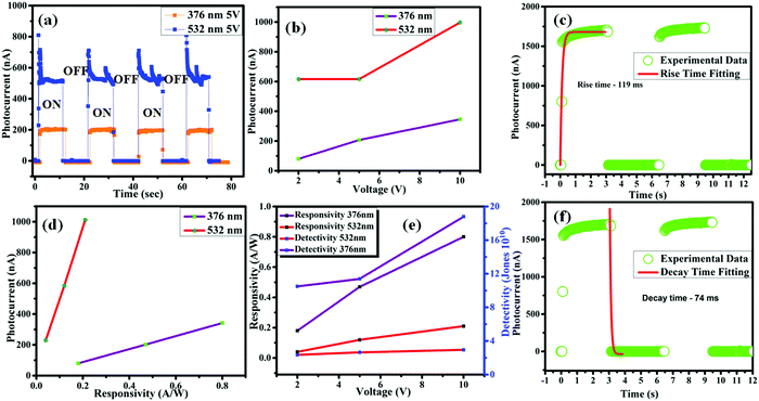 |
| | Fig. 4 (a) Time dependent photocurrent response at a fixed voltage of 5 V, (b) the voltage dependent photocurrent, (d) the responsivity and the photocurrent, and (e) the voltage versus the detectivity and the responsivity. (c) and (f) Show the representative rise and fall time fitting. | |
Table 2 Transient photocurrents for the FAPbBr2I perovskite single crystal
| Laser |
Bias voltages |
Responsivity |
Detectivity |
| 376 nm |
10 V |
0.80 A W−1 |
1.81 × 10¹¹ Jones |
|
|
5 V |
0.47 A W−1 |
1.14 × 10¹¹ Jones |
|
|
2 V |
0.18 A W−1 |
1.05 × 10¹¹ Jones |
| 532 nm |
10 V |
0.21 A W−1 |
2.95 × 10¹⁰ Jones |
|
|
5 V |
0.12 A W−1 |
2.63 × 10¹⁰ Jones |
|
|
2 V |
0.04 A W−1 |
2.35 × 10¹⁰ Jones |
5 Conclusions
A FA-based lead halide single-crystal of FAPbBr2I was successfully grown. The energy band gap for the mixed halide perovskite single crystal lies between FAPbI3 and FAPbBr3, which paves the way for the growth of perovskite single-crystals for their application in optoelectronic devices owing to the influence of the halide content. The structural characterization confirmed that it was a single crystalline in nature. The peak photocurrent 1 μA was achieved under a bias applied voltage of 10 V, and the corresponding responsivity and detectivity reached the maximum values, using a visible (376 nm) laser, of 0.8 A W−1 and 1.81 × 10¹¹ Jones, respectively. This study could significantly improve the applications of perovskite single-crystals and low temperature-based optoelectronic devices, including solar cells.
Conflicts of interest
There are no conflicts to declare.
Acknowledgements
The authors would like to thank EPSRC POLARIS HOUSE (EPSRCPH) for financial support under the SUNRISE (Strategic University Network to Revolutionise Indian Solar Energy) grant number (RP03541). The author (RG) also thanks to the Council of Scientific and Industrial Research (CSIR) New Delhi, India, for providing the senior research fellowship (31/001(0451)/2016-EMR-I).
References
- A. Kojima, K. Teshima, Y. Shirai and T. Miyasaka, J. Am. Chem. Soc., 2009, 131, 6050–6051 CrossRef CAS PubMed.
- O. J. Weber, D. Ghosh, S. Gaines, P. F. Henry, A. B. Walker, M. S. Islam and M. T. Weller, Chem. Mater., 2018, 30, 3768–3778 CrossRef CAS.
- H. Chen, F. Ye, W. Tang, J. He, M. Yin, Y. Wang, F. Xie, E. Bi, X. Yang, M. Grätzel and L. Han, Nature, 2017, 550, 92–95 CrossRef CAS PubMed.
- S. Arya, P. Mahajan, R. Gupta, R. Srivastava, N. kumar Tailor, S. Satapathi, R. R. Sumathi, R. Datt and V. Gupta, Prog. Solid State Chem., 2020, 100286 CrossRef CAS.
- H. J. Yen, P. W. Liang, C. C. Chueh, Z. Yang, A. K. Y. Jen and H. L. Wang, ACS Appl. Mater. Interfaces, 2016, 8, 14513–14520 CrossRef CAS.
- T. Zhang, M. Yang, E. E. Benson, Z. Li, J. Van De Lagemaat, J. M. Luther, Y. Yan, K. Zhu and Y. Zhao, Chem. Commun., 2015, 51, 7820–7823 RSC.
- S. Wang, Y. Jiang, E. J. Juarez-Perez, L. K. Ono and Y. Qi, Nat. Energy, 2017, 2, 1–8 Search PubMed.
- M. L. Lai, F. Deschler, H. J. Snaith, T. Bein, D. Credgington, Z.-K. Tan, F. Hanusch, A. Sadhanala, R. S. Moghaddam, R. Higler, M. Price, P. Docampo, R. H. Friend and L. M. Pazos, Nat. Nanotechnol., 2014, 9, 687–692 CrossRef PubMed.
- J. W. Lee, D. J. Seol, A. N. Cho and N. G. Park, Adv. Mater., 2014, 26, 4991–4998 CrossRef CAS PubMed.
- Z. Li, M. Yang, J. S. Park, S. H. Wei, J. J. Berry and K. Zhu, Chem. Mater., 2016, 28, 284–292 CrossRef CAS.
- T. Matsushima, F. Bencheikh, T. Komino, M. R. Leyden, A. S. D. Sandanayaka, C. Qin and C. Adachi, Nature, 2019, 572, 502–506 CrossRef CAS PubMed.
- H. Algadi, C. Mahata, B. Sahoo, M. Kim, W. G. Koh and T. Lee, Org. Electron., 2020, 76, 105444 CrossRef CAS.
- Z. Song, H. Zhou, P. Gui, X. Yang, R. Liu, G. Ma, H. Wang and G. Fang, J. Mater. Chem. C, 2018, 6, 5113–5121 RSC.
- J. Zhou and J. Huang, Adv. Sci., 2017, 5, 1700256 CrossRef PubMed.
- Z. Yang, J. Dou, M. Wang, J. Li, J. Huang and J. Shao, J. Mater. Chem. C, 2018, 6, 6739–6746 RSC.
- M. Zhang, F. Zhang, Y. Wang, L. Zhu, Y. Hu, Z. Lou, Y. Hou and F. Teng, Sci. Rep., 2018, 8, 1–9 Search PubMed.
- W. Tian, H. Zhou and L. Li, Small, 2017, 13, 1702107 CrossRef.
- S. S. Rong, M. B. Faheem and Y. B. Li, J. Electron. Sci. Technol., 2021, 19, 1–18 Search PubMed.
- D. Shi, V. Adinolfi, R. Comin, M. Yuan, E. Alarousu, A. Buin, Y. Chen, S. Hoogland, A. Rothenberger, K. Katsiev, Y. Losovyj, X. Zhang, P. A. Dowben, O. F. Mohammed, E. H. Sargent and O. M. Bakr, Science, 2015, 347, 519–522 CrossRef CAS PubMed.
- P. K. Nayak, D. T. Moore, B. Wenger, S. Nayak, A. A. Haghighirad, A. Fineberg, N. K. Noel, O. G. Reid, G. Rumbles, P. Kukura, K. A. Vincent and H. J. Snaith, Nat. Commun., 2016, 7, 1–8 Search PubMed.
- R. Gupta, T. B. Korukonda, S. K. Gupta, B. P. Dhamaniya, P. Chhillar, R. Datt, P. Vashishtha, G. Gupta, V. Gupta, R. Srivastava and S. Pathak, J. Cryst. Growth, 2020, 537, 125598 CrossRef CAS.
- M. I. Saidaminov, A. L. Abdelhady, G. Maculan and O. M. Bakr, Chem. Commun., 2015, 51, 17658–17661 RSC.
- P. F. Ndione, Z. Li and K. Zhu, J. Mater. Chem. C, 2016, 4, 7775–7782 RSC.
- Z. Chen, Q. Dong, Y. Liu, C. Bao, X. Xiao, Y. Bai, Y. Deng, J. Huang, Y. Fang, Y. Lin, S. Tang and Q. Wang, Nat. Commun., 2017, 1–7 Search PubMed.
- Y. Fang, H. Wei, Q. Dong and J. Huang, Nat. Commun., 2017, 8, 1–9 CrossRef CAS PubMed.
- T. Kirchartz, F. Staub and U. Rau, ACS Energy Lett., 2016, 1, 731–739 CrossRef CAS.
- X. Zhang, C. Liu, G. Ren, S. Li, C. Bi, Q. Hao and H. Liu, Nanomaterials, 2018, 8, 1–10 Search PubMed.
- S. Li, S. Tong, J. Q. Meng, C. Zhang, C. Zhang, J. Shen, S. Xiao, J. Sun, J. He, Y. Gao, B. Yang and J. Yang, Org. Electron., 2018, 52, 190–194 CrossRef CAS.
- J. Song, L. Xu, J. Li, J. Xue, Y. Dong, X. Li and H. Zeng, Adv. Mater., 2016, 28, 4861–4869 CrossRef CAS PubMed.
- L. Chu, R. Hu, W. Liu, Y. Ma, R. Zhang, J. Yang and X. Li, Mater. Res. Bull., 2018, 98, 322–327 CrossRef CAS.
- Q. Han, S. H. Bae, P. Sun, Y. T. Hsieh, Y. Yang, Y. S. Rim, H. Zhao, Q. Chen, W. Shi, G. Li and Y. Yeng, Adv. Mater., 2016, 28, 2253–2258 CrossRef CAS PubMed.
- D. Arquer, X. Gong, R. P. Sabatini, M. Liu, G. Kim, B. R. Sutherland, O. Voznyy, J. Xu, Y. Pang, S. Hoogland, D. Sinton and E. Sargent, Nat. Commun., 2017, 8, 14757 CrossRef PubMed.
- M. Cao, J. Tian, Z. Cai, L. Peng, L. Yang and D. Wei, Appl. Phys. Lett., 2016, 109, 233303 CrossRef.
- G. Maculan, A. D. Sheikh, A. L. Abdelhady, M. I. Saidaminov, A. Haque, B. Murali, E. Alarousu, O. F. Mohammed, T. Wu and O. M. Bakr, J. Phys. Chem. Lett., 2015, 19, 3781–3786 CrossRef PubMed.
Footnote |
| † Electronic supplementary information (ESI) available. See DOI: 10.1039/d1ma01096d |
|
| This journal is © The Royal Society of Chemistry 2022 |
Click here to see how this site uses Cookies. View our privacy policy here. 
 Open Access Article
 This Open Access Article is licensed under a Creative Commons Attribution-Non Commercial 3.0 Unported Licence
 *c,
Ram
Datt
*c,
Ram
Datt