
 Open Access Article
 This Open Access Article is licensed under a Creative Commons Attribution-Non Commercial 3.0 Unported Licence
Multi-layered composites using polyurethane-based foams and 3D-printed structures to curb electromagnetic pollution†
Kumari
Sushmita
 a,
Subhasish
Maiti
b and
Suryasarathi
Bose
*b
a,
Subhasish
Maiti
b and
Suryasarathi
Bose
*b
aCentre for Nanoscience and Engineering, Indian Institute of Science, Bangalore-560012, India
bDepartment of Materials Engineering, Indian Institute of Science, Bangalore-560012, India. E-mail: sbose@iisc.ac.in
First published on 20th April 2022
Abstract
Herein, a comparative study of the electromagnetic interference (EMI) shielding performance of multi-layered architectures fabricated using different strategies (i.e., polyurethane (PU)-based film, foam, and 3D printed structures) has been evaluated. The key attributes, i.e., conductivity and various losses towards efficient attenuation of the incoming EM radiation, were achieved by incorporating multiwalled carbon nanotubes (CNTs) and ferrite-decorated reduced graphene oxide (rGO–Fe3O4) strategically in the multi-layered structure. To fabricate the multi-layered architecture, rGO–Fe3O4 was incorporated in polyvinylidene difluoride (PVDF) and the CNTs in the polycarbonate (PC) as the two outer layers of the architecture. PU-based structures (film or foam or 3D printed mesh) containing CNTs were fabricated and sandwiched between the PC and PVDF composite films to develop multi-layered architecture with improved shielding performance. The novelty of this work lies in the fabrication and shielding study of such porous-layered composite structures and comparing them with non-porous counterparts. The results suggested that amongst all the fabricated structures, the PU–CNT foam-based multi-layered structure showed a high shielding effectiveness (SET) value of −39 dB in the K-band, with absorption-dominated shielding (91% and above). In order to further enhance the shielding effectiveness, Ag was sputtered on the PU-foam, which resulted in the highest SET value of −50 dB in the X-band. The results presented here begin to suggest that in-situ synthesized foam with non-uniform and dead pores enhances the shielding performance compared to 3D printed mesh structures or non-porous structures.
1. Introduction
Electromagnetic interference (EMI) is when the functioning of one electronic device is influenced by the other nearby devices/instruments. EMI leads to signal perturbation during communication and data loss, which might eventually lead to system failure. Thus, a shielding material is required to block unwanted electromagnetic (EM) radiations from affecting the devices under operation. In a quest to resolve the issue of EMI, several strategies have been adopted, from purely metal-based EMI shields to polymer composite-based EMI shields and also the hybrid of the two approaches.1–4 There has been a significant advancement in designing materials for EMI shielding in the last decade. The data shows that the number of publications related to EMI, its health hazards, and shielding has increased 180–330% during 2007–2017 period.5EMI Shielding, expressed in the units of dB, is a summation of losses due to reflection, absorption, and multiple reflections.6 Bulk metals are the most conventional choice for EMI shielding applications because of free electrons, which reflect the incoming EM wave. However, metals and their reflection-based shielding are acceptable in some scenarios but not all (e.g., walls of the anechoic chamber) as it leads to stray radiations in the vicinity of the shield. Also, most metals suffer from drawbacks such as high density, corrosion, and processing/design difficulty.4,7 To cater to the demand for absorption-based shielding and the ease of designing complex shapes and structures, polymer composites gained popularity.8 The electric, dielectric and magnetic properties in polymer composites can be tuned. One can obtain a reflection or absorption-based shield depending upon the type of nanofillers, its dispersion, and the shield's design. To enhance the microwave absorption properties, the lossy (dielectrically and magnetically) nanofillers are often added along with conductive nanofillers in the polymer matrix.6 The interfaces at the polymer–nanofiller junction also lead to multiple scattering and interfacial polarization losses.9 Many of these polymer composites have flame resistivity, hydrophobic nature, and some specific polymer composites also exhibit self-healing characteristics, an added advantage in terms of applicability.10–17 The tunable electrical–dielectric–magnetic properties, corrosion resistivity, and ability to be shaped into complex structures make polymer composites suitable for several electronic packaging applications where EMI shielding is a necessity.6
Metal, transition metal oxides, and carbon-based nanofillers are the three most commonly used fillers to enhance the effective shielding in polymer-based materials.6,7,18 High aspect ratio carbon nanostructures, such as carbon nanotubes (CNTs), are highly favored nanofiller. CNTs have oxidation resistance, are lightweight, and form conductive network structures at low nanofiller concentrations.6 In addition, carbon nanostructures possess high tensile strength and flexibility and many a time tend to impart a reinforcing effect to polymer composites but within a limited range of concentration.6 The different forms of carbon-based fillers used in EMI shielding applications include CNTs, carbon black, graphite, reduced graphene oxide (rGO), graphene nanoplatelets (GNPs), etc.6,19,20 Apart from these, metal nanofillers (e.g., Ag nanowire, Cu nanostructures, etc.), oxide-based nanofillers (e.g., ZnO, TiO2, BaTiO3, etc.), magnetic nanofillers (e.g., Ferrites, Fe, Ni, Co, and their alloys) and MXenes are often efficient in either enhancing the total shielding or absorption percentage of the total shielding.19–21 A combination of CNT and rGO–Fe3O4 has been employed as fillers in this work. CNTs, their high electrical conductivity, and dielectric properties make them suitable for EMI shielding applications. rGO–Fe3O4 serves as an EMI shielding filler due to its dielectrically and/or magnetically lossy nature.18 It has also been reported that graphene and ferrite nanoparticles result in defect and interfacial polarization, and their coupling adds to the absorption loss.22,23 Also, both CNT and rGO–Fe3O4 enhance the thermal conductivity of the composites.22,24
Besides the nature and distribution of nanofillers in the polymer matrix, the shield design is another parameter influencing the EMI shielding performance. Recent researches in this field have seen a shift from simple composite structures to multi-layered composite structures, foam-based structures, and three-dimensional (3D) printed composite structures.5,25 Multi-layered/sandwiched structures can efficiently control the distribution of nanofillers and thus the formation of the conductive pathway. The multiple interfaces can lead to scattering and polarization losses. Researchers have obtained high EMI shielding performance at low filler content using the multi-layered approach than the composites prepared by common methods.25,26 This strategy also allows tuning the absorption percentage through a rational arrangement of conductive and magnetic filler layers to construct a controllable electromagnetic gradient.26–28 In contrast, porous structures enhance the shielding properties at low filler volume fraction due to filler localization in the solid portion, the air traps, and scattering at multiple interfaces.25 3D foamed polymer composites exhibit low density, large specific surface area, and high porosity, making them suitable for shielding applications in fields such as automobiles and spacecraft. Furthermore, well-designed cell structures can also be obtained using 3D printing technology, a more controllable and repeatable approach to designing porous structures.29–32
3D printing technique was invented a few decades back but now finds usage in various sectors such as aerospace (e.g., aircraft components), biomedical (e.g., implants, scaffolds), electronics (e.g., sensors and actuators), robotics, etc.33–41 3D printing of polymers for EMI shielding applications is a relatively newer area but has been growing for a couple of years.30–32,42–47 In a recent work by Ning Chen et al.,43 they fabricated 3D printed mesh structure (honeycomb geometry) using conducting filament (made up of CNT/graphene nanosheets/PLA). They concluded that a pore size less than 1/5th of incident wavelength (λ/5) is recommended for a lightweight shield with desirable EMI shielding performance. In an earlier work by Yinghong Chen et al.,30 they performed an EMI shielding study using a mesh structure made up of conducting filament with different cell geometries and cell sizes. They concluded that cell geometry had a negligible impact on EMI shielding performance, but with decreasing cell size, EMI shielding increased. Recently, Xing et al.32 prepared CNT/chitosan-based ink and 3D printed square mesh structures for EMI shielding applications. They also simulated and analysed the influence of pore size and conductivity of the composites on the EMI shielding performance for a square hole grid structure. They concluded that for non-magnetic material, conductivity has a more significant influence on the EMI shielding performance than the pore size. Further, to find the maximum pore size (a) for optimum shielding, they did a theoretical calculation (refer to eqn (1)) based on Maxwell and Helmholtz equations (with certain assumptions).32 According to their analysis, when the test EMI frequency range was 8.2–12.4 GHz, with fmax of 12.4 GHz, the relative permeability for non-magnetic material kept as 1, vacuum permeability (μ0) as 4π × 10−7 H m−1, vacuum permittivity (ε0) as 8.854 × 10⁻¹² F m−1 and the relative permittivity kept as 12–14; the square hole size of shielding material should not be more than 3.23 mm. Here 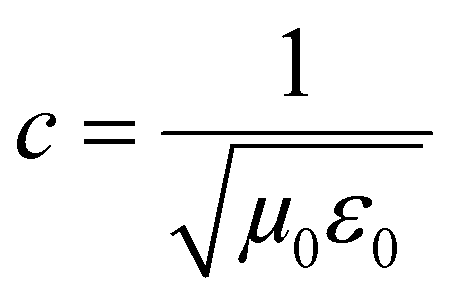 is the speed of light in a vacuum.
 | (1) |
We observe that the value for the pore size obtained in this particular case is equivalent to approximately (λ/7.5). The available literature thus gives an approximate idea of the target pore size for enhancing EMI shielding performance.
PU has been 3D printed for various applications (biomedical implants, stretchable electronics, etc.) primarily because of its flexibility and biocompatibility.48–50 More recently, 4D printing of shape memory PU composites has been targeted because of the tunable properties arising from the hard and soft segments in PU structure.48 However, to the best of our knowledge, this is the first time PU-based 3D printed designs have been fabricated for EMI shielding applications. It is to be noted that 3D printing of PU using fused deposition modeling (FDM) approach is tricky and requires specific temperature and printing speed optimization to minimize material clogging and filament buckling.48
Foams have been extensively studied for EMI shielding applications in the last decade.51–53 In the work by Ding et al.51 published in 2020, they showed a comparison of various composite foams. The SET was found to vary from −7 dB in epoxy-based composite foams (∼2.8 mm thick), −18 dB in polyimide-based composite foams (∼0.5 mm thick), −17 dB in polyetherimide-based composite foams (∼2.5 mm thick), −13 dB in polymethylmethacrylate-based composite foams (∼2.5 mm thick) to −31 dB in PU-based composite foams (∼3 mm thick).51 In a recent review article published by Wang et al.,52 they showed polymer-based composite foams, fabricated using polymers such as epoxy, polymethylmethacrylate, PU, PVDF, high density polyethylene and poly(L-lactic acid), and fillers such as Fe3O4, CNT, graphene-based ones. Amongst the polymer-based composite foams reported in this review article,52 most of them were fabricated using the supercritical CO2 foaming technique and a highest SET of −58 dB was obtained for PU/graphene (10 wt%) foam with a thickness of 60 mm. PU-based foams and composite foams can be easily fabricated at the lab and industrial scale and find a wide range of applications extending from the household, automotive, packaging to electronics and aerospace.54 PU-based composite foams with fillers such as CNT, graphene nanosheets, graphite, rGO, and other hybrid fillers have been widely explored for EMI shielding applications.51,52,55,56 Conducting and/or lossy fillers in PU foam enhances the EMI shielding performance, and certain carbonaceous fillers in PU foam may also exhibit a mechanical reinforcing effect.54
In this work, multi-layered structures were designed in such a way that PU-based thin film or porous structures were sandwiched between the two composite films. As already stated, multi-layered strategy and porous structure are known to enhance EMI shielding performance due to the scattering and polarization losses from multiple interfaces. Here, the porous structures have been fabricated by two approaches, one by synthesis and the other by using 3D printing technology. For comparison, a multi-layered structure with non-porous PU of the same thickness has also been evaluated. As already stated, PU-based foams have been well studied for several applications, including EMI shielding.54–59 However, this work explored a unique strategy to effectively evaluate and assess the multi-layered porous structures. A combination of porous structures with multi-layering has hardly been explored. Also, a comparative study of such multi-layered porous and non-porous structures has not yet been reported. Below are the research details of our work.
• A comparative study of different types of PU-based structures for EMI shielding, i.e., PU-based thin films, foams, and 3D printed structures, has been performed. In the first approach, PU-based film is sandwiched between PC composite film and PVDF composite film (refer to row 1 in Fig. 1). In the second approach, PU-based synthesized foam is sandwiched between PC composite film and PVDF composite film (refer to row 2 in Fig. 1). And in the third approach, the PU-based 3D printed mesh structure is sandwiched between PC composite film and PVDF composite film (refer to row 3 in Fig. 1). As control experiments, PU-based thick non-porous block is sandwiched between PC composite film and PVDF composite film (refer to row 4 in Fig. 1).
 | ||
| Fig. 1 Schematic of the various configurations (with their nomenclature) of multi-layered structures under study in this work. | ||
• Comparison of multi-layering without metal (refer to columns 1 and 2 of Fig. 1) versus multi-layering with a metal layer (here Ag sputtered layer, refer to columns 3 and 4 of Fig. 1) has also been performed.
It is worth mentioning that three different polymers (PC, PU and PVDF) have been used for layering. PC has been chosen as it has a low percolation threshold (<0.5 wt%) for CNTs.60 Being a ductile polymer, PVDF can incorporate a large amount of hybrid filler such as rGO–Fe3O4 without much structural deterioration. PU selection as a porous structure is based on the fact that it is easy to synthesize PU and fabricate foam/composite foam structures using PU.54
2. Experimental section
2.1 Materials
PC (Lexan 143 R, MFI-11 g/10 min, Mw = 37![[thin space (1/6-em)]](https://www.rsc.org/images/entities/char_2009.gif) 492, Mn = 20642, PDI = 1.8) was purchased from Sabic. PVDF was bought from Arkema (Kynar 761 grade, Mw ∼ 440000 g mol−1). PU 3D printing filament was bought from Wol3D. DGEBA (diglycidal ether of bisphenol-A) epoxy pre-polymer with an amine-based hardener system was bought from Atul industries. Pristine multiwalled carbon nanotube (CNT) material, NC7000 (length 1.5 μm and diameter 9.5 nm), was procured from Nanocyl SA (Belgium). Graphene oxide (GO) powder (BTGOX) was purchased from BT Corp. Ferric chloride hexahydrate (FeCl3·6H2O) was bought from Thomas Baker. 4,4′-Methylenebis(phenyl isocyanate) (or MDI, molecular weight = 250.25 g mol−1) was procured from Sigma Aldrich. 1,4 butanediol was purchased from Spectrochem Pvt. Ltd. Polyethyleneglycol 4000 (PEG) flakes were purchased from SRL chemicals. Hydrazine hydrate (H4N2·H2O) (99%), ethylene glycol (C2H6O2), and urea (NH2CONH2) were procured from SDFCL. Chloroform, tetrahydrofuran (THF), and dimethylformamide (DMF) were procured from SDFCL. Analytical grade absolute ethanol was procured from Changshu Hongsheng Fine Chemical Co., Ltd.
492, Mn = 20642, PDI = 1.8) was purchased from Sabic. PVDF was bought from Arkema (Kynar 761 grade, Mw ∼ 440000 g mol−1). PU 3D printing filament was bought from Wol3D. DGEBA (diglycidal ether of bisphenol-A) epoxy pre-polymer with an amine-based hardener system was bought from Atul industries. Pristine multiwalled carbon nanotube (CNT) material, NC7000 (length 1.5 μm and diameter 9.5 nm), was procured from Nanocyl SA (Belgium). Graphene oxide (GO) powder (BTGOX) was purchased from BT Corp. Ferric chloride hexahydrate (FeCl3·6H2O) was bought from Thomas Baker. 4,4′-Methylenebis(phenyl isocyanate) (or MDI, molecular weight = 250.25 g mol−1) was procured from Sigma Aldrich. 1,4 butanediol was purchased from Spectrochem Pvt. Ltd. Polyethyleneglycol 4000 (PEG) flakes were purchased from SRL chemicals. Hydrazine hydrate (H4N2·H2O) (99%), ethylene glycol (C2H6O2), and urea (NH2CONH2) were procured from SDFCL. Chloroform, tetrahydrofuran (THF), and dimethylformamide (DMF) were procured from SDFCL. Analytical grade absolute ethanol was procured from Changshu Hongsheng Fine Chemical Co., Ltd.
2.2 Synthesis of Fe3O4 decorated reduced graphene oxide
Fe3O4 decorated reduced graphene oxide (rGO) was synthesized using a solvothermal synthesis protocol mentioned in our previous work.26 Ferric chloride hexahydrate was used as the iron source. With the help of urea and hydrazine hydrate in the ethylene glycol solvent, the salt was reduced to Fe3O4. This oxide formation took over rGO sheets (derived from commercial GO) during the solvothermal process. The SEM micrographs of rGO–Fe3O4 can be found in Fig. S1 (ESI†). However, a detailed structural characterization and magnetic property study related to the rGO–Fe3O4 can be found in our previous work.262.3 Preparation of PU-based non-porous structures, foams, and 3D printed structures
:MDI:butanediol was kept as 1:(n + 1):n, similar to the one reported by LeÓn et al.61 The final stoichiometry of reactants was chosen through a trial-and-error experiment where we varied ‘n’ from 2 to 6. The synthesized PU showed somewhat poor mechanical properties at a lower value of ‘n’ (brittle while handling). Hence ‘n’ was kept as 5 in the final experiment. The expected reaction mechanism for PU synthesis is shown in Fig. 3.61 The –OH group in PEG acts as a nucleophile and attacks the –NCO group's electrophilic C in MDI to yield a polymer with urethane linkage. This synthesized polymer is PU (refer to step1, Fig. 3). This PU can be further reacted with the chain extender (butanediol) to enhance its mechanical properties (refer to step2, Fig. 3).
2.3.1.1 Preparation of neat PU film/block. In a typical synthesis of neat PU, 2 mmol of PEG was dissolved in 60 ml DMF at 50 °C with N2 purging, as shown in Fig. 2. Thereafter, 12 mmol of MDI was added, and the entire system was kept under N2 environment. The temperature was slowly increased to 100 °C, and after 1 h, butanediol (10 mmol) was dropwise injected into the solution. The reaction was stirred at 100 °C under N2 environment (with reflux) for 24 h. N2 environment is essential to prevent the reaction of the isocyanate group with air moisture. The viscosity increase can be observed during the reaction, indicating polymer formation. The viscous reaction product was poured into a Teflon plate and dried. Subsequently, the dried PU pieces were compression molded (with Teflon sheets on both sides) for different thicknesses at 160 °C to obtain a thin film or thick block (digital image of the film is shown in Fig. S2a, ESI†).
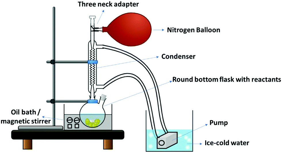 | ||
| Fig. 2 Experimental setup for the PU synthesis. | ||
2.3.1.2 Preparation of PU-CNT film/block. The synthesis protocol of PU-CNT was similar to that of neat PU, except that CNTs were initially added to the reaction mixture. CNTs were added into 100 ml DMF and bath sonicated to obtain a well-dispersed solution. PEG, MDI, and butanediol were added, and subsequent processing was similar to that mentioned in the previous section. It is to be noted that the solvent in the case of PU–CNT synthesis is higher than that of neat PU synthesis. This is because CNTs tend to make the entire solution too viscous, and extra solvent is required for better dispersion of CNTs and dissolution of reactants. It is worth noting that CNT concentration was fixed (through trial and error, confirmed by TGA) to 3–3.5 wt% with respect to PU. The digital image of PU-CNT compression molded film is shown in Fig. S2b (ESI†).
2.3.2.1 Preparation of neat PU foam. PU neat foams (digital image shown in Fig. S2d, ESI†) were synthesized using PEG and MDI (no chain extender) in the molar ratio 1
:7. In a typical synthesis, 2 mmol of PEG was dissolved in 30 ml DMF at 50 °C with N2 purging. Thereafter, 12 mmol of MDI was added, and the entire system was kept under N2 environment. The temperature was slowly increased to 100 °C, and an instant viscosity rise was observed. It was then followed by solidification of the reaction product to give a foam-like structure. Thereafter, it was kept under a vacuum at 60 °C to remove the remnant solvent that resulted in a porous rigid structure. The higher molar ratio of PEG:MDI and the less solvent quantity (as compared to Section 2.3.1.1) was probably the reason for the rapid viscosity rise leading to solidification with solvent traps in it. The removal of solvent through vacuum drying further resulted in a porous structure. In the case of foam synthesis, reaction step 1 (shown in Fig. 3) itself resulted in semi-rigid foam after vacuum drying.
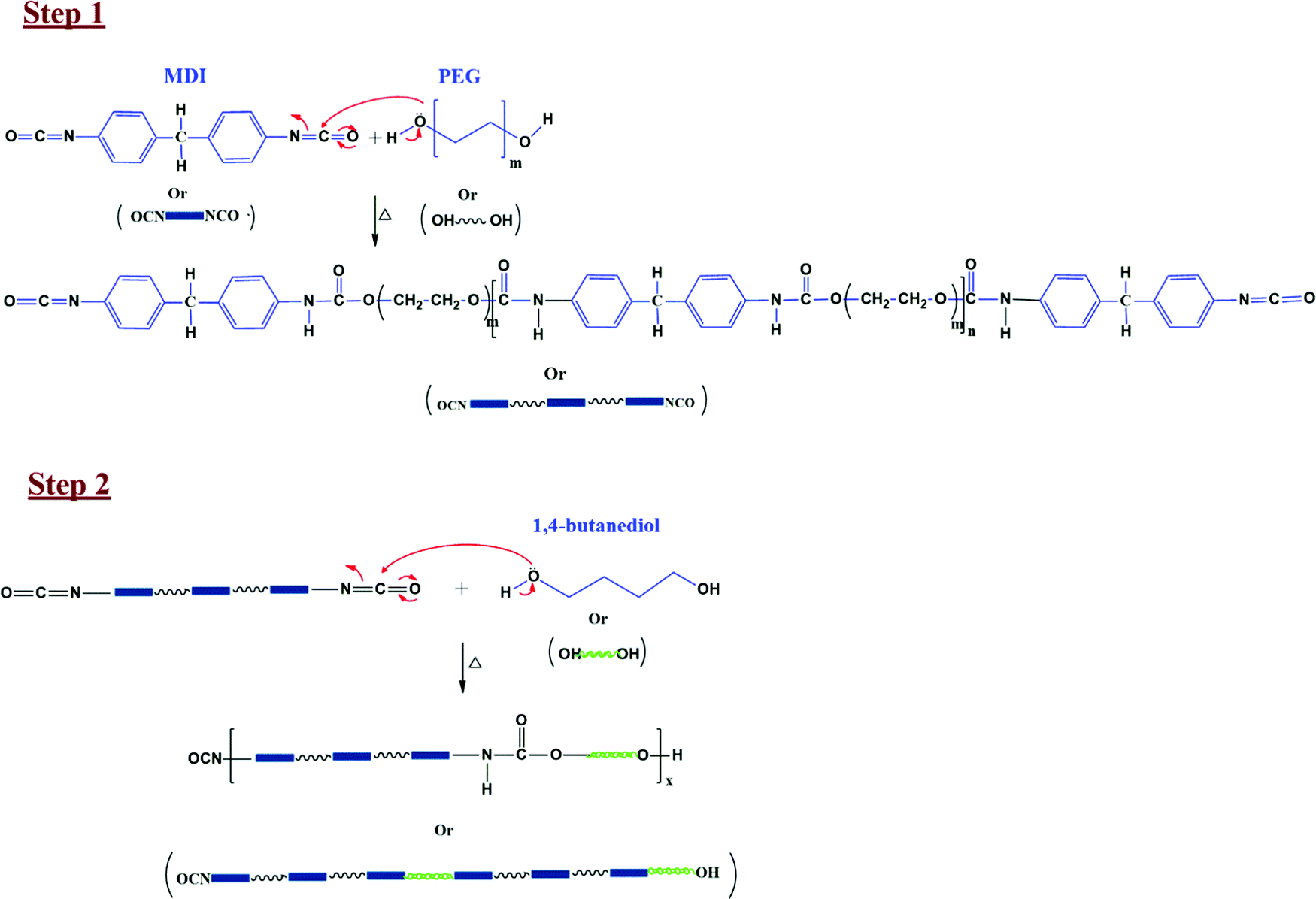 | ||
| Fig. 3 Reaction mechanism involved in the synthesis of PU. | ||
2.3.2.2 Preparation of PU-CNT foam. The synthesis protocol was similar to neat PU foam, except that CNTs were initially added to the reaction mixture. CNTs were added into 60 ml DMF and bath sonicated to obtain a well-dispersed solution. PEG and MDI (molar ratio = 1
:7) were then added to the reaction mixture at 50 °C with N2 purging, and the subsequent synthesis process was similar to that of PU foam. Again, it is to be noted that the solvent quantity is higher than that mentioned in neat PU foam synthesis. Also, CNT concentration was fixed (through trial and error, confirmed by TGA) to 3–3.5 wt% with respect to PU. The digital image of PU-CNT foam is shown in Fig. S2e (ESI†).
2.3.3.1 Preparation of neat PU 3D printed structure. An effort was made to replicate the foam structure using 3D printing technology (FDM). The mesh design (shown in Fig. 4) was printed using a commercially bought neat PU filament. For the mesh design, 1 mm diameter holes were cut, extruded in a helical pathway across the thickness. The helical pathway was chosen as an attempt to give a tortuous pathway to the incoming EM wave. As PU filament is flexible, 3D printing was challenging as the filament was getting stuck during processing. At a print speed of 30–40 mm s−1, nozzle temperature of 220 °C, and bed temperature of 65 °C, we performed the 3D printing successfully. The digital image of the neat PU 3D printed structure is shown in Fig. S2g (ESI†).
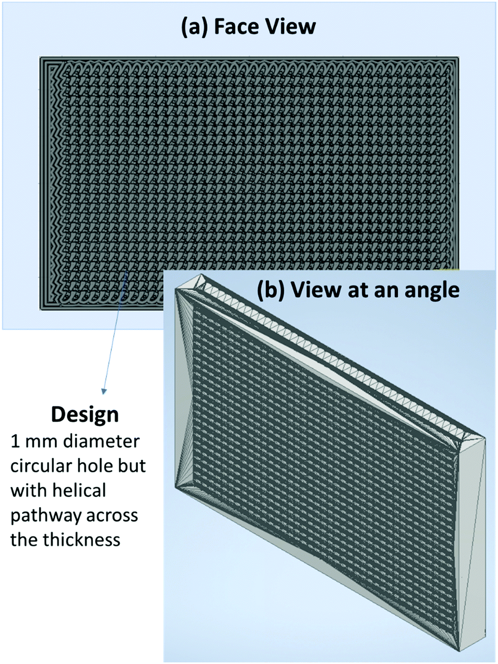 | ||
| Fig. 4 The mesh design for 3D printing (a) face view, (b) view at an angle. | ||
2.3.3.2 Preparation of PU-CNT 3D printed structure. CNT was dispersed in THF by probe sonication followed by bath sonication. The neat PU 3D printed structure was dip-coated in CNT-THF dispersion. Since THF is a solvent for PU, CNT adhered well to the 3D printed structure. However, care is to be taken that dip-coating should be done quickly, and the dip coated-3D printed structure should immediately be desiccated; otherwise, the structure will collapse. Also, CNT concentration was fixed (through trial and error, confirmed by TGA) to 3–3.5 wt% with respect to PU. The digital image of the PU-CNT 3D printed structure is shown in Fig. S2h (ESI†).
Since the PU–CNT foam-based multi-layered structure showed the best performance in terms of total shielding effectiveness (SET) and absorption percentage, PU–CNT foam was also sputter-coated with Ag to study the combined effect of Ag and CNT.
2.4 Preparation of the multi-layered structures
As shown in Fig. 1, several multi-layered structures were fabricated for a comparative study of EMI shielding performance. To obtain the multi-layered structure, PU-based film, block, foam, and 3D printed structure were individually sandwiched between composite sheets of PC+ 3 wt% CNT (or PC–CNT film) and PVDF+ 10 wt% rGO–Fe3O4 (or PVDF–rGO–Fe3O4 film). PC–CNT film was chosen as one of the face sheets because PC has a low percolation threshold for CNTs and has CNT has a reinforcing effect on PC.60,62 The PVDF–rGO–Fe3O4 film was chosen as another face sheet as PVDF is a film-forming polymer. It easily incorporates a high content of fillers such as rGO–Fe3O4, which is both magnetically and dielectrically lossy.60 The digital images of PC–CNT film and PVDF–rGO–Fe3O4 film are shown in Fig. S3 (ESI†). Fig. S3 (ESI†) also depicts that though neat PC is known to be brittle, incorporating CNT into PC reinforces the thin PC–CNT film (more flexible).Since there are several configurations of multi-layered structures, we will label them for simplicity. Hereon, PVDF/PU film/PC denotes that neat PU film is sandwiched between PVDF–rGO–Fe3O4 film and PC–CNT film. It is to be noted that in all such multi-layered nomenclatures, we haven’t explicitly mentioned the fillers (rGO–Fe3O4, CNT) in PVDF and PC for simplicity, but they do exist, i.e., in all the multi-layered structures, PC always has CNT incorporated into it, and PVDF always has rGO–Fe3O4 incorporated in it. Hence by this convention, only the middle term in nomenclature (shown in Fig. 1) changes in each configuration depending upon the choice of the middle layer, i.e., PU film, PU–CNT film, PU–Ag film, PU foam, PU–CNT foam, PU–Ag foam, PU–CNT–Ag foam, PU 3D print, PU–CNT 3D print, PU–Ag 3D print, PU block, and PU–CNT block.
3. Characterizations
Scanning electron microscopy (SEM) and energy-dispersive X-ray spectroscopy analysis (EDS) was performed using a Carl Zeiss Ultra 55 FE-SEM. The SEM samples were coated with a few nm of Au to prevent charging in the electron beam. Ag sputter deposition was done using the Anelva RF magnetron sputtering unit (Model SPF 332H) in the presence of Ar gas. The 3D printer (Model-Creality Cr10s Pro) and PU 3D printing filament used in this work were bought from Wol3D. The thermogravimetric analysis (TGA) of polymers/polymer composites was performed in a platinum pan using TGA Q500 (from TA instruments) under N2 atmosphere. Fourier transform infrared (FTIR) spectroscopy was done using an FTIR instrument bought from PerkinElmer. Universal attenuated total reflectance mode (ATR) was used to obtain % transmittance in the wavenumber range of 4000–650 cm−1. The room temperature AC conductivity study was measured using Alpha-A Analyser (Novocontrol, Germany) in a broad range of frequencies varying from 10−1 to 107 Hz. The film samples of diameter 10 mm were used as specimens, and bulk electrical conductivity measurement was performed across the thickness. EMI shielding interference was studied using the keysight fieldfox microwave analyzer N9918A in the frequency range of 8.2–26.5 GHz. S-Parameters (S11, S12, S21, S22) were obtained from vector network analyzer (VNA), which were then used to obtain the SET and shielding effectiveness due to reflection (SER) and absorption (SEA).4. Results and discussions
4.1 Spectroscopic analysis of the films, foams, and 3D printed structures
The synthesized PU and PU-CNT films, as well as foams, were examined using FTIR spectroscopy, as shown in Fig. 5a and b. The spectra of PU film versus PU-CNT film and PU foam versus PU-CNT foam were similar, suggesting that the CNTs are physically trapped inside PU. When comparing the film versus foam spectra, there were no significant differences in the spectra, except that a few peaks (C![[double bond, length as m-dash]](https://www.rsc.org/images/entities/char_e001.gif) O, C–N) were more intense, suggesting the possibility of more crosslinking leading to the foamability of PU.
O, C–N) were more intense, suggesting the possibility of more crosslinking leading to the foamability of PU.
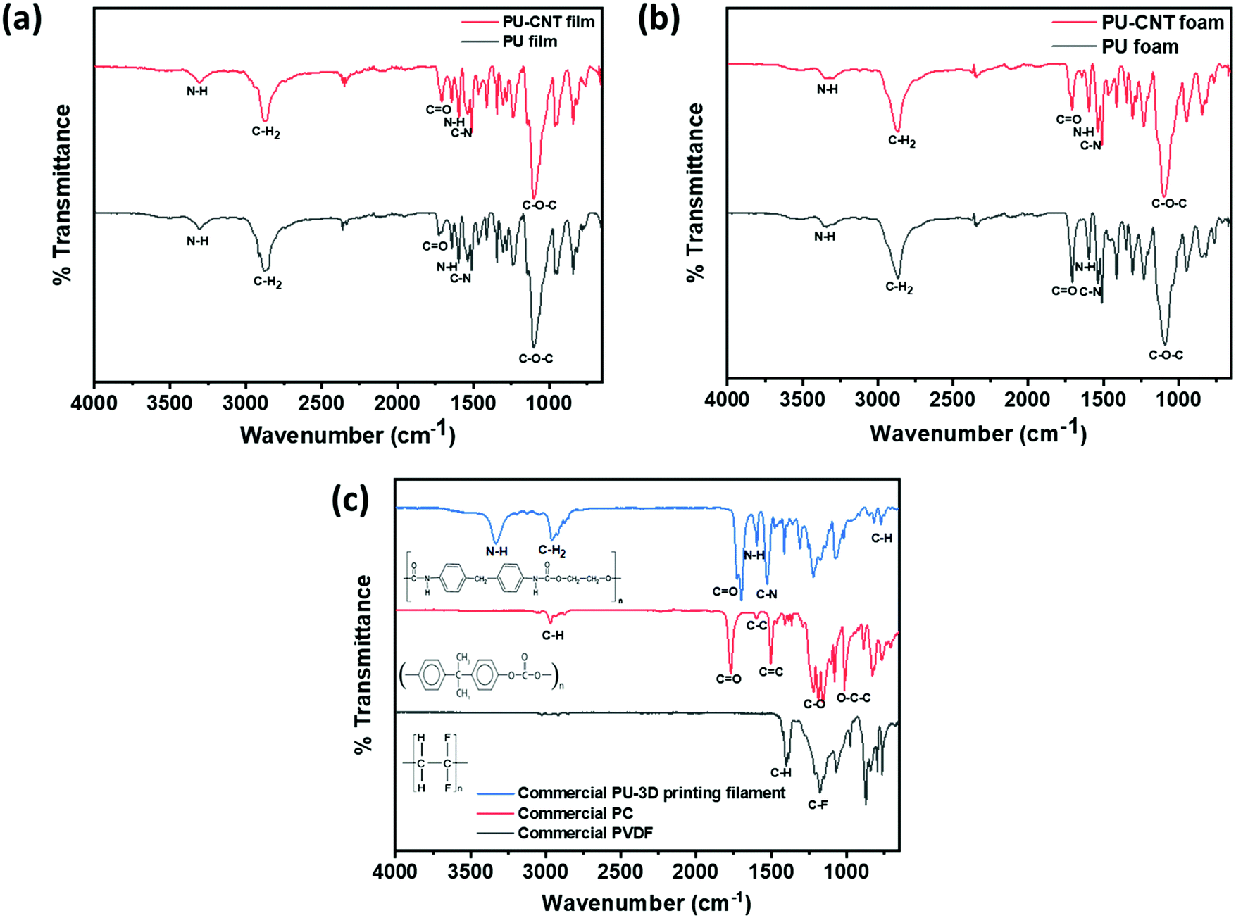 | ||
| Fig. 5 FTIR spectra for (a) PU film and PU-CNT film, (b) PU foam and PU-CNT foam, (c) commercial PVDF, PC, and PU-3D printing filament. | ||
Fig. 5a and b show the typical absorption bands of the urethane group. The absorption peak observed in the range 3302–3355 cm−1 corresponds to the symmetric and the asymmetric stretching vibrations of N–H due to the isocyanate segment of urethane.61,63–65 The medium-strong peak at 1595 cm−1 corresponds to the in-plane bending vibration of N–H.61 The stretching vibrations of the ester CO are depicted by the sharp absorption peaks in the range 1700–1730 cm−1. The peak in the range of 900–700 cm−1 represents the out-of-plane bending vibration of C–H in multi-substituted benzene ring.61 The polyols peak can be observed around 2865–2880 cm−1, corresponding to the C–H2 stretching vibrations.61 The broad and strong peak at around 1100 cm−1 corresponds to the ether bond C–O–C stretch.61 The peak at 1535 cm−1 is assigned to the C–N bond, and it supports the synthesis of urethane.61,65 In addition, the absence of absorption peak in the range 2255–2275 cm−1 indicates that the initial –NCO has completely reacted during synthesis of PU.61,64 The peaks typical of PU can also be observed in the FTIR spectra of commercial PU-3D printing filament shown in Fig. 5c.
Fig. 5c also shows the FTIR spectra of commercial PC and commercial PVDF used in this work. The FTIR spectra of PC show the characteristic absorption peaks of PC. The peak observed around 2970 cm−1 corresponds to the C–H (aromatic ring) deformations.66,67 The peak around 1770 cm−1 depicts the carbonyl CO stretch.67,68 The absorption peak at 1600 cm−1 can be assigned to the stretching vibration of the C–C bond arising from the phenyl group (benzene ring), and the peak at 1504 cm−1 corresponds to the CC bond vibration.66 The stretching of the ester group (C–O or O–C–O) is observed in the range of 1165–1232 cm−1.66,69 Lastly, carbonates contain the O–C–C group, whose asymmetric stretch can be observed at 1015 cm−1.69 Similarly, the FTIR spectra of PVDF confirm its characteristic peaks. The strong band at 1402cm−1 is attributed to the stretching vibration of C–H bonds, and the absorption band at 1178cm−1 can be assigned to the vibration of C–F bonds.70
4.2 CNT loaded PU composites and their thermal stability
TGA was performed to determine the degradation temperature and CNT concentration in PU film/block, foam, and 3D printed structure, as shown in Fig. 6. The synthesized PU has a comparatively lower degradation temperature than the 3D-printed PU made of a commercial PU filament. The onset of degradation for PU film and foam is between 250–260 °C, while the onset of degradation for 3D printed structure is ∼270 °C. Also, the incorporation of CNT in the synthesized PU matrix has brought only minor enhancement (2–4 °C) in the degradation temperature, as observed in Fig. 6a and b. In the case of 3D printed structures, CNT has a negligible impact on the degradation temperature of composite. This might be due to CNT coating only on the exposed surface of the 3D printed structure and not within the structure. From Fig. 6, it is evident that both synthesized and 3D printed PU-based samples degraded completely below 400 °C. Since CNT has a higher decomposition temperature of ∼480 °C,71 the difference of residue between PU and PU–CNT in the temperature range of 400–480 °C can be an approximate measure of the CNT content in PU. After a few trial experiments, we were able to fix the content of CNT to 3–3.5 wt%. This is confirmed by observing the difference in residue between PU and PU-CNT at 450 °C. The difference is approximated to be equivalent to the percentage of CNT contained in the PU matrix.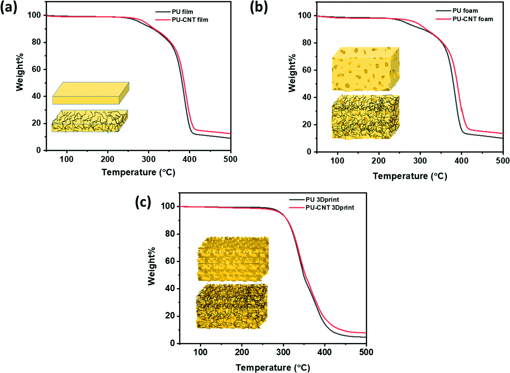 | ||
| Fig. 6 TGA for (a) PU film and PU–CNT film, (b) PU foam and PU–CNT foam, (c) PU 3Dprint and PU–CNT 3Dprint. | ||
4.3 Morphological analysis of the single-layered and multi-layered structures
This section highlights the surface morphology of the single-layered and multi-layered structures. For this purpose, we have performed the SEM and EDS of a few representative samples to gain insight into the surface feature and thickness of the structure. Fig. 7 shows the single-layered PC–CNT film (refer to Fig. 7a and b) and single-layered PU-CNT film (refer to Fig. 7c and d). These SEM samples were prepared via cryofracture and coating with a few nm of Au. The CNTs in PC (refer to Fig. 7b) appear as the thread-like white feature. While in Fig. 7d, CNTs appear as white dots on the surface of PU. It is to be noted that CNTs being conducting in nature tend to appear brighter in SEM. Fig. S4a and b (ESI†) show the digital images of PC–CNT and PU–CNT film, respectively. From these bulk images of the sample, non-uniform dispersion of CNTs is observed in PU–CNT film compared to PC–CNT film. Fig. 8 shows the SEM and EDS of synthesized PU film sputtered with Ag. As shown in Fig. 8e, one side of this film is sputtered with Ag and has a dense Ag concentration at the edge. The thickness of all the individual film samples was optimized within the range of 0.2–0.35 mm. It is difficult to precisely confirm the thickness of the Ag sputtered layer through atomic force microscopy or optical profilometry as the base polymer substrate is not even, and the error itself is in the range of a few hundred nanometres. However, EDS of Ag suggests a strong presence of Ag on the edge of PU film for a few hundred nanometres. It is to be noted that sputtering of PU-based foams and 3D printed structure were done under the same conditions and thus are expected to have the same Ag layer thickness.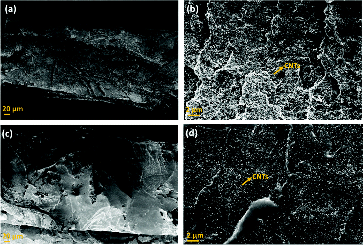 | ||
| Fig. 7 Scanning electron micrograph of (a) PC–CNT film (low magnification), (b) PC–CNT film (high magnification), (c) PU–CNT film (low magnification), and (d) PU–CNT film (high magnification). | ||
 | ||
| Fig. 8 (a) Scanning electron micrograph of PU–Ag film, (b) Scanning electron micrograph of PU–Ag film under consideration for EDS analysis, (c) EDS mapping: C map, (d) EDS mapping: O map, (e) EDS mapping: Ag map. | ||
Fig. 9 shows the SEM of the multi-layered film, foam and 3D printed structure, namely PVDF/PU film/PC (Fig. 9a), PVDF/PU foam/PC (Fig. 9b), and PVDF/PU 3Dprint/PC (Fig. 9c). The SEM samples were prepared by cutting the multi-layered structures with a razor blade and coating it with a few nm of Au. The cross-section was observed, and the overall thickness of PVDF/PU film/PC is ∼1 mm, while that of PVDF/PU foam/PC and PVDF/PU 3Dprint/PC was kept as ∼5.3 mm. Some voids at the interface were observed but only at a few locations. This might be due to the insufficient epoxy or the artifact created while preparing the SEM samples using a razor blade. The PU foam in Fig. 9b shows some dead pores of variable sizes (0.2–1.3 mm) on its surface. The 3D printed structure in Fig. 9c was designed to replicate foam by making a tortuous helical pathway. As a result, the cross-sectional view of the 3D printed structure shows asymmetric pores of sizes 0.7–1.3 mm. In this work, the highest frequency under study (for EMI shielding performance) is 26.5 GHz, which corresponds to λ ∼ 11.3 mm. The pore size range in foam and 3D printed structures is thus kept less than λ/7.5 (obtained under certain assumptions) as well as λ/5 as suggested in the existing works of literature.32,43 The SEM of PU–CNT foam and PU–CNT 3Dprint is shown in Fig. S5 (ESI†). Compared to neat PU foam (shown as the mid-layer in Fig. 9b), the PU-CNT foam surface (shown in Fig. S5a, ESI†) is rough with comparatively more nano- and micro-pores, apart from the regular macropores. Compared to the neat PU 3D printed structure (shown as the mid-layer in Fig. 9c), PU-CNT 3D printed structure (shown in Fig. S5b, ESI†) showed smoother edges, probably due to the coating of CNTs on the exposed surface. It is to be noted that we increased the thickness of PU-film to obtain PU non-porous block and further fabricated a multi-layered structure using the same, i.e., PVDF/PU block/PC (∼5.3 mm). However, SEM of only PVDF/PU film/PC has been presented for simplicity.
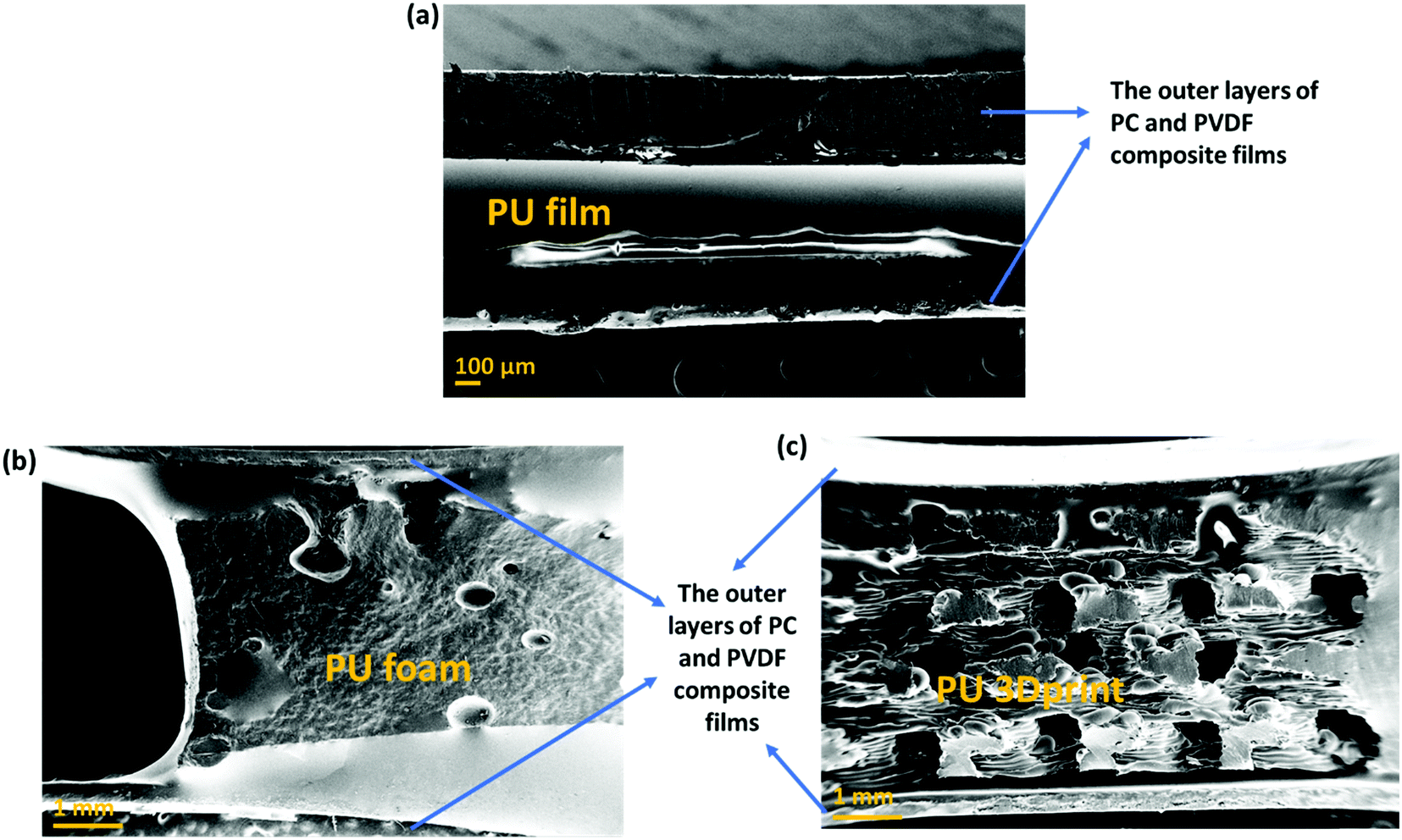 | ||
| Fig. 9 Scanning electron micrograph of (a) PVDF/PU film/PC, (b) PVDF/PU foam/PC and (c) PVDF/PU 3Dprint/PC. | ||
The SEM-EDS of the multi-layered film, foam, and 3D printed structure are shown in Fig. S6–S8 (ESI†), respectively. The SEM-EDS demonstrates various elements (C, O, F, Fe) in the respective layers. Additionally, the porosity of the various porous structures was calculated using the Archimedes method and shown in Table S1 (ESI†). The foam-based structures are found to be more porous compared to 3D-printed structures. It is to be noted that this technique provides the estimate of porosity and is primarily based on water retention within the porous structures.
4.4 Electrical and EMI shielding properties of the fabricated structures
This section will discuss the electrical properties and the EMI shielding performance of the fabricated structures. Since foams and 3D printed structures have porosity, the bulk electrical conductivity measurement isn’t feasible. Hence, the electrical conductivity of only the individual films is measured. Thereafter, we have discussed the EMI shielding performance and the percentage shielding via absorption/reflection to understand the role of fillers/coating and the architecture on the shielding mechanism.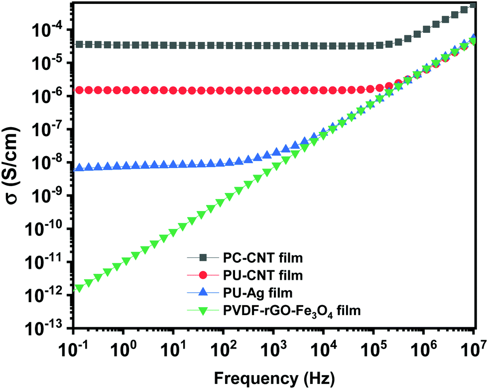 | ||
| Fig. 10 AC electrical conductivity as a function of frequency. | ||
The rest of the films in Fig. 10 shows a frequency-independent plateau at lower frequency following the universal power-law fitting as per eqn (2).72,73Eqn (2) explains the variation of AC Conductivity with frequency and is observed in complex systems with multiple phases as in composite materials or heterogeneous systems. The bulk ac conductivity has a frequency-independent response at low frequencies in a typical curve. This is because of the percolated path of resistors across the network. Here, the ac conductivity of the capacitors is sufficiently low, and current flows through the resistor percolation path. However, at higher frequencies, the ac conductivity increases as per the power law due to the increasing conductivity of the capacitors.
 | (2) |
The exponent “s” varies in the range of 0–1 and depends on temperature and frequency. It depicts the extent of charge transfer that occurs through tunneling/hopping. It measures the degree of connectedness of long-range charge hopping pathways or the extent of tortuosity for mobile charges.74 It is to be noted that polymer/CNT composite exhibits ohmic conduction in a continuous conductive path, equivalent to the current through the resistor.32 However, when a polymer spacing exists between two CNTs (similar to a capacitor), charge transfer is via hopping or tunneling.75 The dominant conduction mechanism can be decided from the dispersion and distribution of CNTs in the polymer matrix, which strongly depends on the concentration of CNTs in the matrix and matrix–CNT interaction. When the mean CNT–CNT distance is below 10 nm, the dominant electron transfer mechanism is the tunneling mechanism, whereas above that hopping mechanism is dominant.
The frequency-independent plateau (σ(0) or σDC, refer to eqn (2)) represents the dc electrical conductivity of the composite film. The σDC value of around 1 S m−1 (or 0.01 S cm−1) is considered optimum for good EM absorption performance.76 It is to be noted that CNTs are known to be conducting, and the incorporation of CNT in the polymer matrix enhances the electrical conductivity of the composite. But the content of CNT in the polymer matrix cannot be increased indefinitely because of the processing difficulties. Here, PC–CNT film showed the highest dc electrical conductivity (3.6 × 10⁻⁵ S cm−1) indicating better connectivity of the CNT network than PU-CNT film (1.5 × 10⁻⁶ S cm−1). Though PU–Ag film has Ag sputtering only on one side of the film, it still shows a bulk electrical conductivity plateau at 6.3 × 10⁻⁹ S cm−1. This poor bulk conductivity might be due to the slight diffusion of Ag metal across the thin PU film, as also observed in EDS mapping. However, the surface conductivity of the Ag sputtered layer is expected to be much higher (in order of 105 S cm−1) as Ag is metal.77
Next, the power-law fitting was done, and the nature of the fitting curve is typical of the resistor–capacitor (R–C) networks. The R–C network represents a microstructure containing dielectric (the capacitor) and conductive regions (the resistor).78 By fitting the power law, “s” is found to be 0.97 for PU–Ag film, 0.90 for PU–CNT film, and 0.84 for PC–CNT film, indicating that the charge transfer occurs via hopping.79 The fitting also suggests that the capacitor content decreases from 97% for PU–Ag film to 84% for PC–CNT film. The decrease in the capacitance part in PC–CNT film confirms well-connected CNT conductive pathways in the PC matrix, contributing to the resistive component of the R–C network.
 | (3) |
EMI shielding is contributed from three different mechanisms, namely shielding via reflection (SER), shielding via absorption (SEA), and shielding via multiple reflections (SEMR).
| SET = SEA + SER + SEMR | (4) |
If SET > 15 dB or when the shield thickness is greater than the skin depth, SEMR can be ignored, and thus SET can then be expressed as,
| SET = SEA + SER | (5) |
 | (6) |
 ,
,  and
and  can be further estimated from eqn (7), (8) and (9), respectively.22,81
 | (7) |
 | (8) |
 | (9) |
The electrical conductivity is also related to the imaginary part of permittivity (ε′′) according to eqn (10).22,76,84 It is revealed that when the permittivity meets the EM impedance match requirement, higher dielectric loss implies better EM absorption properties.76
 | (10) |
SET is experimentally estimated using scattering parameters (S11, S12, S21, and S22) obtained from VNA. The scattering parameters are converted to SET, SEA and SER using the equations mentioned below.
 | (11) |
 | (12) |
 | (13) |
Fig. 11 shows SET as a function of frequency for single layers of PU-based structures in X-, Ku- and K-band. It is to be noted that different fixtures are used to obtain SET in various bands, so there is some discontinuity in values at 12.4 GHz and 18 GHz, which may be attributed to the instrumental error. The neat PU film showed negligible SET (shown in Fig. 11a) at all frequencies suggesting that thin PU film by itself has inferior EMI shielding property. The SET of PU 3D printed structure was similar to that of PU non-porous block (refer to Fig. S9a and Table S2, ESI†). Amongst the PU single-layered structures (without fillers), neat PU foam showed the highest SET (approx. −10 dB in K-band, shown in Fig. 11a). With the incorporation of CNT as nanofiller, the SET value increased, as shown in Fig. 11b. The maximum enhancement was observed in PU–CNT foam, which showed a SET value of approx. −30 dB at 26.5 GHz. These results indicate that foam-based structures with non-uniform and dead pores enhance the shielding performance due to the trapped air, adequate impedance match between the air and material surface, and enhanced multiple scattering due to numerous pore walls and interfaces.86 PU–CNT 3D printed structure (refer to Fig. 11b) had CNT only on the exposed surface, and it showed a similar SET value as PU–CNT block (refer to Fig. S9a, ESI†), which had CNT throughout the bulk. The 3D printed replica of in situ foam is thus not advantageous over the non-porous PU block in terms of SET enhancement. Additionally, the shielding performance of PC–CNT film and PVDF–rGO–Fe3O4 film is shown in Fig. S10a (ESI†). Fig. S10b (ESI†) shows the bar plot of the real and imaginary components of permittivity and permeability for PC–CNT and PVDF–rGO–Fe3O4 at 26.5 GHz frequency. Using these permittivity (ε′ and ε′′) and permeability (μ′ and μ′′) values, tanδε (dielectric loss factor), tanδμ (magnetic loss factor), total tanδ (total relative loss), impedance match characteristics, and attenuation constant were calculated (refer to Fig. S10c and d, ESI†). It is worth noting that the impedance match was enhanced, and the total tanδ was found to be higher for PVDF–rGO–Fe3O4 than PC–CNT, confirming the lossy nature of rGO–Fe3O4. However, the attenuation constant was higher for PC–CNT, which also exhibited a higher SET value. Also, it is observed that SET mostly increases with frequency across different frequency bands (as one moves from X-band to K-band, refer to Fig. 11a and b).
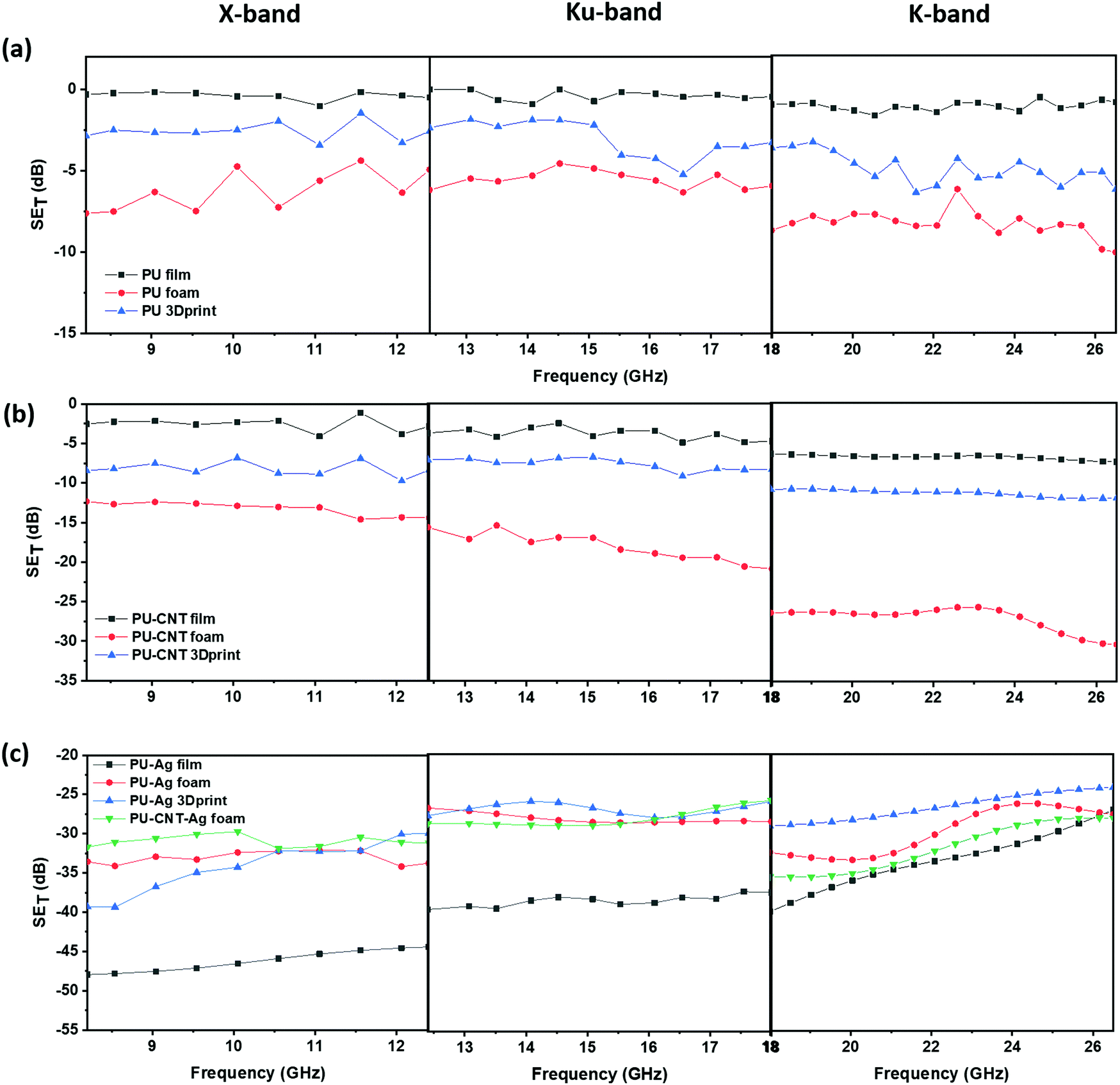 | ||
| Fig. 11 SETvs. frequency for single layers of PU-based structures: (a) PU film, PU foam and PU 3Dprint structure in X-, Ku- and K-band; (b) PU–CNT film, PU–CNT foam and PU–CNT 3Dprint structure in X-, Ku- and K-band; (c) PU-Ag film, PU–Ag foam and PU–Ag 3Dprint structure in X-, Ku- and K-band. | ||
A few representative samples were coated with Ag to understand the impact of Ag on shielding performance. Compared to CNT, a layer of Ag metal sputtering on the neat PU-based structure led to a drastic enhancement in SET, as shown in Fig. 11c. This is because metals act as EMI shields due to the presence of free electrons. Bulk metals such as Al sheet or Cu sheet are known to be EM reflectors.87 However, in this work, we are trying to understand the impact of sputtering a thin layer of Ag on the EMI shielding performance and how the performance differs if the layer of Ag is sandwiched between the polymer composite films. Also, shielding behavior comparison of metal layering (here Ag) on polymer vs. carbonaceous high aspect ratio nanofiller (here CNT) incorporation in the polymer matrix is much needed. It is to be noted that unlike the bulk metal, the sputtering technique coats a thin film of Ag over the substrate as a result of bombardment of the target Ag metal by energetic plasma particles. However, techniques such as sputtering are cost-intensive. Its usage for applications in EMI shielding is less industry-friendly due to the additional infrastructure and huge expenditure required for large-scale production. As observed in Fig. 11c, the PU–Ag film, PU–Ag foam, and PU–Ag 3Dprint structure showed SET values higher than ∼−24 dB at all frequencies. At some frequencies, the SET value was observed to be in the range of −40 to −48 dB. Metal-based samples showed high fluctuations during measurement, and hence commenting on its frequency dependence is rather tricky. But the Ag sputtered layer increases the SET value drastically even at low shield thicknesses, as observed in PU–Ag film. From the SET study in Fig. 11c, we observe that when Ag is coated, total shielding efficiency is dominated by the Ag layer rather than the porosity or thickness. Since PU–CNT foam showed the highest SET value among the CNT-based samples, it was further chosen for Ag sputtering to understand the combined effect of CNT incorporation and Ag layering. But from the SETvs. frequency plots in Fig. 11c, we observe that PU–Ag foam and PU–CNT–Ag foam showed similar EMI shielding performance. This once again confirms the dominance of Ag over the CNT. In Section 4.4.3, the percentage absorption–reflection study will be discussed, wherein we will get into the details of the shielding mechanism in all the fabricated structures.
Fig. 12 shows SET as a function of frequency for multi-layered structures in X-, Ku- and K-band. Fig. 12a shows the multi-layered structures without Ag, whereas Fig. 12b shows those with Ag. When the single-layered PU-based structures (results shown in Fig. 11) are incorporated as sandwiched layers in a multi-layered structure (results shown in Fig. 12), the SET is enhanced in most cases. This is because PC and PVDF flat sheets have CNT and rGO–Fe3O4 as the conducting and lossy filler, respectively. The losses due to fillers and multiple scattering originating due to different layers primarily contribute to the enhancement in SET in a multi-layered structure. In samples with Ag sputtered layer, the SET is once again dominated by the presence of Ag, as all such multi-layered structures showed a SET value of approx. −27 dB and above, at all frequencies.
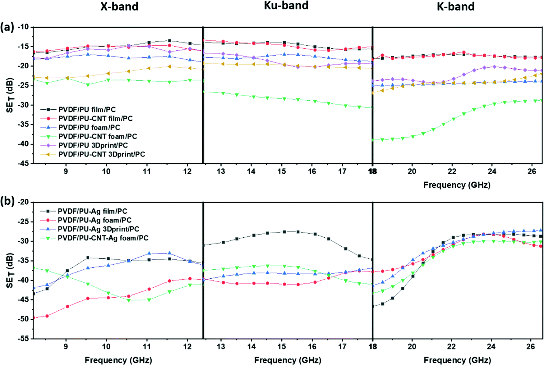 | ||
| Fig. 12 SETvs. frequency for multi-layered structures: (a) without Ag in X-, Ku- and K-band; (b) with Ag in X-, Ku- and K-band. | ||
From Fig. 12, it is evident that the total shielding performance has a negligible influence of the incorporation of CNT in PU film-based multi-layered structures (refer to the plot of PVDF/PU film/PC and PVDF/PU–CNT film/PC in Fig. 12a). This can be attributed to the lower thickness of the film and the poor connectivity of CNT in PU–CNT film. However, in a multi-layered structure with foams, CNT incorporation in foam has significantly enhanced SET value. The SET value in PVDF/PU–CNT foam/PC is as high as −39 dB at 18 GHz frequency. This can be possibly attributed to the combined effect of CNTs connectivity in foam and the porosity of PU–CNT foam-based structure. The SET value of multi-layered structures with PU 3Dprint, PU–CNT 3Dprint, PU block, and PU–CNT block is mostly in between the multi-layered film-based structures and foam-based structures (refer to Fig. 12 and Fig. S9a, Table S3, ESI†). The results suggest that PU–CNT foam having non-uniform dead pores proved to be a better shielding material than the artificially designed 3D printed structure (the one shown in Fig. 4). Also, in the case of PU–CNT foam, CNT is distributed in the entire foam matrix; however, in the case of PU–CNT 3Dprint, CNT lies only on the exposed surface as the preparation method was dip coating. Consequently, the multiple scattering in PU–CNT foam (CNT is distributed throughout the matrix) should be much more than the PU–CNT 3D printed structure. From Fig. 12b, it can be further interpreted that in the case of a multi-layered film with an Ag sputtered layer, the SET value is as high as −40 to −50 dB in some frequency ranges. As already mentioned, the dominance of Ag metal can be observed.
The SET value of the composite material depends not only on the design of the shield and the distribution and dispersion of filler/fillers but also on the intrinsic conductivity, dielectric and magnetic properties, and the aspect ratio of filler/fillers.23,24 It is worth noting that conducting nanofiller such as CNTs results in conduction and eddy current losses and the interfacial polarization losses arising from the polymer–CNT interfaces.12,32,88 Whereas rGO–Fe3O4 gives rise to the interfacial polarization losses at the filler/polymer interfaces and also the dielectric and magnetic losses.60,89 The permittivity and permeability analysis of CNT and/or rGO–Fe3O4-based composites have been shown in Fig. S10 (ESI†). CNTs, having a high aspect ratio, result in a conductive network formation in the composite at low filler concentration, thereby contributing to EMI shielding performance. In contrast, functional groups and defects on the large rGO 2D sheet (size ranges up to a few microns) are expected to contribute to the dipole polarization losses.23,89 Further, the large rGO sheet provides enough surface area22 to prevent the agglomeration of Fe3O4 nanoparticles. The coupling between rGO and ferrite can lead to an adequate impedance match and magneto–dielectric absorption losses.22 The high total tanδ and enhanced impedance match (refer to Fig. S10c, ESI†) of rGO–Fe3O4-based composites (compared to PC–CNT composite) further explain the lossy characteristic of the composite.
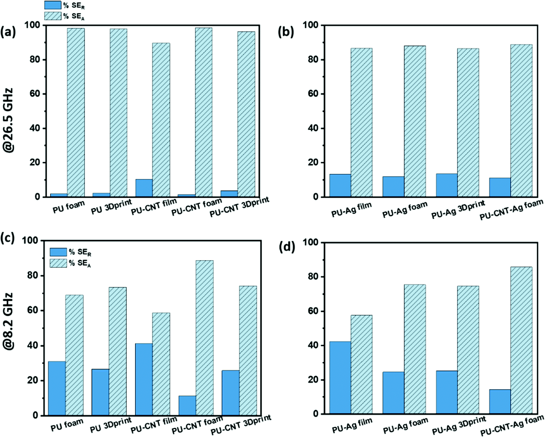 | ||
| Fig. 13 % SEA (light blue bar with stripe pattern) and % SER (dark blue bar with no pattern) for single layers of PU-based structures: (a) without Ag at 26.5 GHz, (b) with Ag at 26.5 GHz; (c) without Ag at 8.2 GHz, (d) with Ag at 8.2 GHz. | ||
 | ||
| Fig. 14 % SEA (light blue bar with stripe pattern) and % SER (dark blue bar with no pattern) at 26.5 and 8.2 GHz: (a and d) with PU-based film as the sandwiched layer in between PVDF–rGO–Fe3O4 film and PC–CNT film; (b and e) with PU-based foam as the sandwiched layer in between PVDF–rGO–Fe3O4 film and PC–CNT film; (c and f) with PU-based 3D print structure as the sandwiched layer in between PVDF–rGO–Fe3O4 film and PC–CNT film. | ||
The percentage absorption-reflection for multi-layered film-based structures (refer Fig. 14a and d), foam-based structures (refer Fig. 14b and e), 3D print-based structures (refer Fig. 14c and f) and block-based control structure (refer to Fig. S9b, ESI†) were analysed. The % SEA is above 64% in all the multi-layered configurations at both frequencies (shown in Fig. 14 and Fig. S9b, ESI†) compared to 53% and above in the case of single-layered structures. From this analysis, we further concluded that the multi-layered structure with PU foam or PU 3D print or PU–CNT foam or PU–CNT 3D print gives 91% and above absorption-based shielding at both 8.2 and 26.5 GHz frequency. The worth of using multi-layered structures instead of single-layered PU-based structures is also significant in these configurations. The enhancement in absorption percentage can be attributed to the porous structure and multi-layering (each layer with different properties), leading to the adequate impedance match and multiple scattering phenomena at layer interfaces, filler–filler interfaces, and filler–polymer interfaces. Porous structure also leads to an increase in propagation path, and the trapped EM wave bounces back and forth inside the shield material.87,90 Since the fillers in each layer are the same in all the configurations, it is primarily the porous architecture resulting in absorption-based shielding. For PVDF/PU–Ag foam/PC, PVDF/PU–CNT–Ag foam/PC, and PVDF/PU–Ag 3Dprint/PC, the presence of Ag metal in the inner layer enhances the reflection percentage of shielding, especially at 8.2 GHz frequency despite the porous structure and multi-layering. It is worth noting that EM wave reflects at an interface with a large difference in impedance, as might be the case in Ag-based structures.87,91 However, in multi-layered structures without Ag, the fillers in layers are either CNT or rGO-based hybrid filler, resulting in a gradual change in conductivity and thus have a comparatively better impedance match than Ag-based structures (refer to Fig. S11c, ESI†).91
Among all the fabricated structures without Ag sputtered layer, PVDF/PU–CNT foam/PC showed the highest SET value of −29 to −39 dB in K-band, with 91% or above absorption dominated shielding (at both 8.2 GHz and 26.5 GHz frequency). Among all the fabricated structures with Ag sputtered layer, PVDF/PU–Ag foam/PC showed the highest SET value (−50 dB @8.2 GHz and −28 to −38 dB in K-band) with 73% or above absorption-based shielding (at both 8.2 GHz and 26.5 GHz frequency). It is to be noted that the thickness of the multi-layered foam-based structures was approx. 5.3 mm. Amongst the multi-layered film-based structures (thickness ∼1 mm), PVDF/PU–Ag film/PC showed the highest SET of −47 dB with 72% or above absorption-dominated shielding (at both 8.2 GHz and 26.5 GHz frequency). It is to be noted that with the incorporation of Ag in the inner layer of multi-layered film/foam, the shielding is dominated by the presence of Ag metal rather than the thickness or porosity of the shield. The schematic of possible loss mechanisms in these three structures is shown in Fig. 15. The key outcomes in EMI shielding performance of the multi-layered configurations are shown in Table S3 (ESI†).
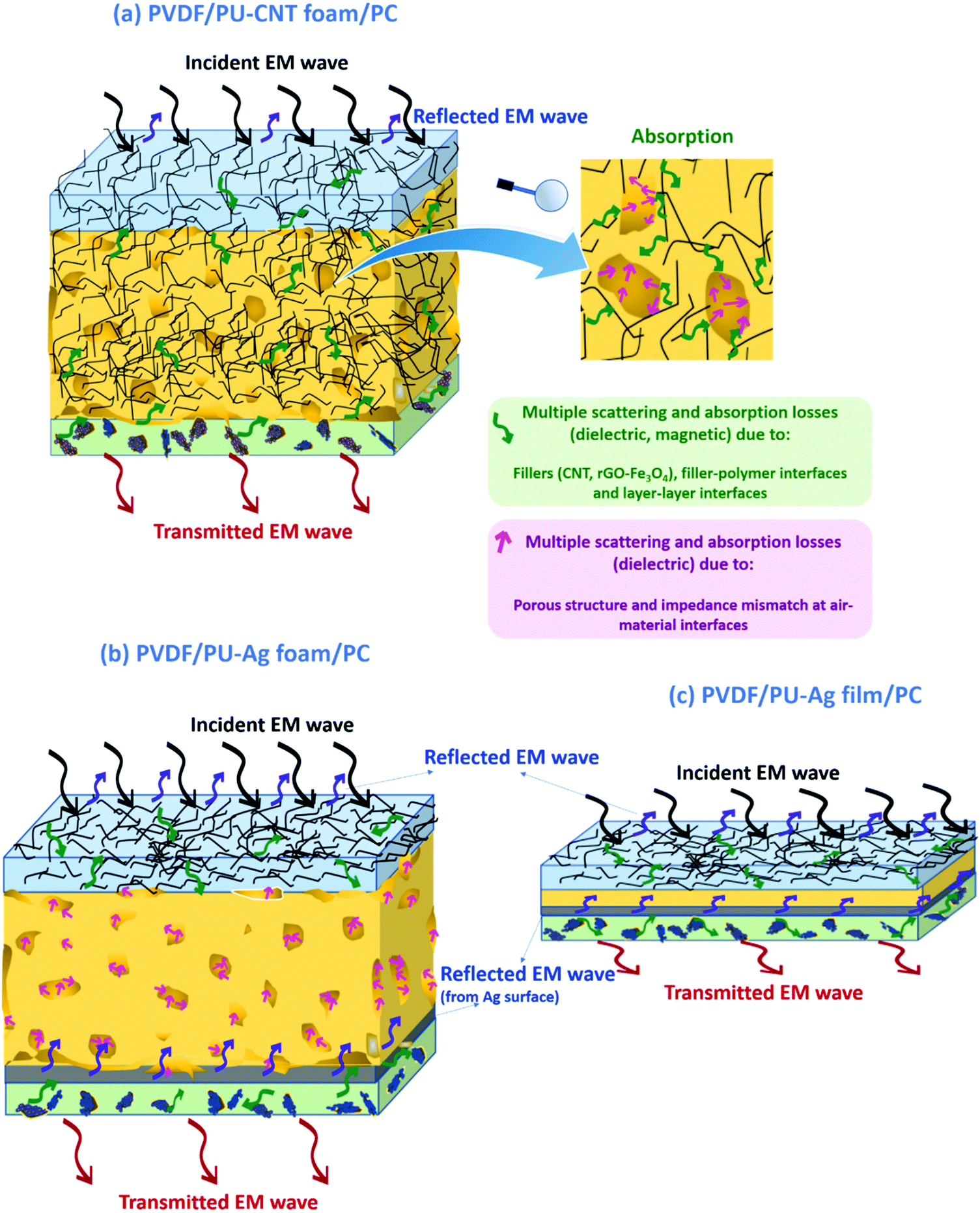 | ||
| Fig. 15 Loss mechanism in (a) multi-layered structure with PU–CNT foam as a sandwiched layer, (b) multi-layered structure with PU–Ag foam as a sandwiched layer, and (c) multi-layered structure with PU–Ag film as a sandwiched layer. | ||
To further understand the mechanism, we also performed the permittivity and permeability study of the multilayered EMI shields (with the best EMI shielding performance) with respect to the control shield at 26.5 GHz frequency (refer to Fig. S11, ESI†). PVDF/PU–CNT foam/PC and PVDF/PU–Ag foam/PC were chosen as the two best representative shields owing to their high SET value. The control shield was the non-porous PVDF/PU–CNT block/PC. Since Ag is highly conducting, the multi-layered structure with Ag showed high permittivity values compared to the other shields (refer to Fig. S11a, ESI†). The total tanδ was found to be high for both PVDF/PU–CNT foam/PC and PVDF/PU–Ag foam/PC (refer to Fig. S11b, ESI†) compared to PVDF/PU–CNT block/PC, suggesting that porous structure enhances the lossy characteristic of the shield, primarily because of the enhancement in dielectric losses (high tan δε). The enhancement in dielectric losses can be primarily attributed to the trapped air and multiple interfaces arising from the porous nature (leading to the dipolar and interfacial polarization losses). The impedance match study suggests that the Ag-based multi-layered structure showed the lowest |Zin/Z0| (approx. 0.24). This might also be the possible cause for a comparatively lower absorption component of shielding in Ag-based shields. The |Zin/Z0| was approx. 0.28 for PVDF/PU–CNT foam/PC, suggesting the highest impedance match and explaining the high absorption performance amongst the selected structures. The attenuation constant values further suggest that the porous multi-layered structures outperform the non-porous multi-layered structure (refer to Fig. S11d, ESI†). Since skin depth is inversely proportional to SEA (refer to eqn (6)), the skin depth is low for PVDF/PU–CNT foam/PC and PVDF/PU–Ag foam/PC compared to PVDF/PU–CNT block/PC (refer to Fig. S11e, ESI†). This implies that the incoming EM wave decays more quickly in porous multi-layered structures compared to the non-porous multi-layered structure. Additionally, the key features of some selected configurations (PU–CNT-based structures, PU–Ag-based structures, and PU–CNT–Ag-based structures) are plotted in Fig. S12 (ESI†).
Fig. 16 depicts the effectiveness of the fabricated EMI shields in blocking the EM waves. For this purpose, we chose two representative multi-layered structures that showed high SET. Among the multi-layered film-based samples, PVDF/PU–Ag film/PC was selected, and among the multi-layered foam and 3D printed samples, PVDF/PU–CNT foam/PC was chosen. A bluetooth module (HC-05) was connected to a mobile phone, and an android application was used to monitor the connectivity of bluetooth. As shown in Fig. 16a, in the absence of an EMI shield, the bluetooth module remained connected to the phone. But when the shield was placed onto the Bluetooth chip in the module, the connectivity was lost, as shown in Fig. 16b and c. This simple experiment further confirms the effectiveness of the developed EMI shields to curb EM pollution.
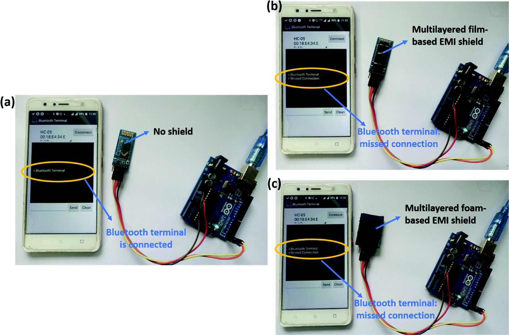 | ||
| Fig. 16 Digital images depicting the effectiveness of the EMI shield developed in this work (a) no shield present, (b) EMI shield (PVDF/PU–Ag film/PC) placed over the chip, (c) EMI shield (PVDF/PU–CNT foam/PC) placed over the chip. | ||
5. Conclusions
In this work, PU and PU in situ CNT thin film was fabricated using polymerization reaction followed by compression molding. Again, through chemical synthesis means, PU and PU in situ CNT foams were fabricated. Further, a 3D printing technique was used to replicate the foam-like structure of PU, and it was dip-coated with CNT to obtain a PU–CNT 3D printed structure. The goal was to figure out how the EMI shielding performance and mechanism of shielding varied with these three different architectures, namely film, foam, and 3D printed structure. As a control, PU non-porous block of the thickness same as foam or 3D printed structure has also been studied. Next, multi-layered architectures were obtained with PC–CNT and PVDF–rGO–Fe3O4 film as outer support layers and PU-based structures as a sandwiched layer between them. Further, Ag sputtering was done on one side of the PU-based structure to understand the role of metal on EMI shielding mechanism and performance and if carbonaceous nanofillers can replace costly techniques such as metal sputtering. The conclusion of this study is mentioned below.• Foam-based PU structures exhibited a higher SET than 3D printed PU mesh, PU non-porous block, and PU thin film. With the incorporation of CNTs, the trend remained the same, i.e., SET for PU–CNT foam > SET for PU–CNT 3D print and non-porous block > SET for PU–CNT film. With Ag sputtering on the PU-based structures, the SET value showed no specific trend implying that the presence of Ag metal dominates and the effect of porosity and thickness on SET is comparatively subsided. However, the % SEA is 75% or above in PU–Ag foam, PU–Ag 3D print, and PU–CNT–Ag 3Dprint at both 8.2 GHz and 26.5 GHz frequency. In contrast, PU–Ag film exhibited a % SEA of 58% or above at 8.2 GHz and 26.5 GHz frequencies. The high reflection component in Ag-based structures can be attributed to the impedance mismatch at the air–Ag interfaces.
• Amongst all the fabricated structures without Ag sputtered layer: PVDF/PU–CNT foam/PC showed the highest SET value of −29 to −39 dB in K-band, with 91% or above absorption dominated shielding (at both 8.2 GHz and 26.5 GHz frequency). The thickness of the structure was approx. 5.3 mm.
• Amongst all the fabricated structures with Ag sputtered layer: PVDF/PU–Ag foam/PC showed the highest SET value (−50 dB @8.2 GHz and −28 to −38 dB in K-band) with 73% and above absorption-based shielding (at both 8.2 GHz and 26.5 GHz frequency). The thickness of the structure was approx. 5.3 mm.
• Amongst the multi-layered film-based structures (thickness ∼1 mm), PVDF/PU–Ag film/PC showed the highest SET of −47 dB with 72% and above absorption-dominated shielding (at both 8.2 GHz and 26.5 GHz frequency).
• The high absorption-dominant shielding in the foam-based multi-layered structure can be attributed to the trapped air, adequate impedance match between air and material's surface, enhanced multiple scattering at layer interfaces (as each layer has different properties) and due to numerous pore walls, filler–filler interfaces, and filler–polymer interfaces.
• The presence of Ag metal enhances the reflection percentage of shielding irrespective of the configuration.
• The in situ synthesized foam with non-uniform and dead pores proved superior in enhancing the SET compared to well-designed 3D printed mesh.
• The % SEA was above 64% in all the multi-layered configurations at both frequencies compared to 53% or above in the case of single-layered structures. The multi-layered strategy has, in most cases, improved the absorption-based shielding when considering both 8.2 GHz and 26.5 GHz frequencies. However, in structures with Ag sputtered layer, the multi-layered strategy need not necessarily be advantageous in enhancing absorption-based shielding. This is because in multi-layered structures without Ag, the fillers in layers are either CNT or rGO-based hybrid filler. There is only a gradual change in conductivity of different layers and thus is expected to have a comparatively better impedance match than Ag-based structures, contributing to absorption dominant shielding.
• The improvement in % SEA for multi-layered strategy can be attributed to the losses due to the flat sheets of PC and PVDF composite films and multiple interfaces. CNTs have a high aspect ratio, resulting in a conductive network formation in PC at a low filler concentration. CNTs result in conduction, eddy current losses, and interfacial polarization losses (from the polymer–CNT interfaces). In contrast, the coupling between rGO and ferrite can lead to an adequate impedance match and magneto–dielectric absorption losses. Also, rGO–Fe3O4 in PVDF contributes to the interfacial polarization losses at the filler/polymer interfaces.
SET of −20 dB or above is acceptable for most commercial applications as it attenuates 99% of the incoming EM signals.6,81,92 In addition, SET of −10 to −30 dB (depends on target application) is considered the minimum effective range suitable for commercial applications.6 If the thickness of the shield can be kept high, carbonaceous fillers perform better in meeting the commercial needs of SET along with high absorption-based shielding (91% and above at both 8.2 and 26.5 GHz). However, when the film thickness is low, metal (such as Ag) layering results in SET as high as −50 dB but has a significant reflection component. For carbonaceous filler to compete with metal layering for low shield thicknesses, one might need to incorporate a high filler concentration in the polymer matrix. This might lead to additional issues such as processing difficulties and poor mechanical properties.
In a recent article by Chen et al.,43 they fabricated 3D printed composite structures and compared them with the existing literature on foam-based composites and composite sheets. The article thus contains a plot of SET values representing the existing literature on such structures. The SET value obtained in our work is comparable to the existing literature43 and has even outperformed in specific configurations. Apart from the excellent EMI shielding performance reported in our work, this study also gives a comparative overview of different design configurations and shielding mechanism, which can help future researchers to choose the shield based on their needs (required shielding performance, thickness of shield, cost, and filler content that can be incorporated).
Conflicts of interest
There are no conflicts to declare.Acknowledgements
The authors would like to acknowledge the funding support from DST-SERB, India. Many thanks to Harshvardhan Gupta and Sumit Kumar for extending their help in 3D printing and Ag sputtering techniques, respectively.References
- H.-C. Lee, J.-Y. Kim, C.-H. Noh, K. Y. Song and S.-H. Cho, Appl. Surf. Sci., 2006, 252, 2665–2672 CrossRef CAS.
- P. Kumar, U. Narayan Maiti, A. Sikdar, T. Kumar Das, A. Kumar and V. Sudarsan, Polym. Rev., 2019, 59, 687–738 CrossRef CAS.
- D. Jiang, V. Murugadoss, Y. Wang, J. Lin, T. Ding, Z. Wang, Q. Shao, C. Wang, H. Liu, N. Lu, R. Wei, A. Subramania and Z. Guo, Polym. Rev., 2019, 59, 280–337 CrossRef CAS.
- D. Wanasinghe and F. Aslani, Composites, Part B, 2019, 176, 107207 CrossRef CAS.
- A. K. Singh, A. Shishkin, T. Koppel and N. Gupta, Composites, Part B, 2018, 149, 188–197 CrossRef CAS.
- S. Sankaran, K. Deshmukh, M. B. Ahamed and S. K. Khadheer Pasha, Composites, Part A, 2018, 114, 49–71 CrossRef CAS.
- D. Wanasinghe, F. Aslani, G. Ma and D. Habibi, Nanomaterials, 2020, 10, 541 CrossRef CAS PubMed.
- D. Markham, Mater. Des., 1999, 21, 45–50 CrossRef.
- J. Sun, W. Wang and Q. Yue, Materials, 2016, 9, 231 CrossRef PubMed.
- T. Wang, W.-C. Yu, C.-G. Zhou, W.-J. Sun, Y.-P. Zhang, L.-C. Jia, J.-F. Gao, K. Dai, D.-X. Yan and Z.-M. Li, Composites, Part B, 2020, 193, 108015 CrossRef CAS.
- A. V. Menon, G. Madras and S. Bose, Chem. Eng. J., 2019, 366, 72–82 CrossRef CAS.
- B. Zhao, R. Wang, Y. Li, Y. Ren, X. Li, X. Guo, R. Zhang and C. B. Park, J. Mater. Chem. C, 2020, 8, 7401–7410 RSC.
- Z. Zeng, W. Li, N. Wu, S. Zhao and X. Lu, ACS Appl. Mater. Interfaces, 2020, 12, 38584–38592 CrossRef CAS PubMed.
- A. Das, H. T. Hayvaci, M. K. Tiwari, I. S. Bayer, D. Erricolo and C. M. Megaridis, J. Colloid Interface Sci., 2011, 353, 311–315 CrossRef CAS PubMed.
- J. Liu, H.-B. Zhang, R. Sun, Y. Liu, Z. Liu, A. Zhou and Z.-Z. Yu, Adv. Mater., 2017, 29, 1702367 CrossRef PubMed.
- C. Liu, S. Ye and J. Feng, Chem. – Asian J., 2016, 11, 2586–2593 CrossRef CAS PubMed.
- L. He, Y. Shi, Q. Wang, D. Chen, J. Shen and S. Guo, Compos. Sci. Technol., 2020, 199, 108324 CrossRef CAS.
- K. Sushmita, G. Madras and S. Bose, ACS Omega, 2020, 5, 4705–4718 CrossRef CAS PubMed.
- R. B. Jagadeesh Chandra, B. Shivamurthy, S. D. Kulkarni and M. S. Kumar, Mater. Res. Express, 2019, 6, 082008 CrossRef.
- N. Wu, Q. Hu, R. Wei, X. Mai, N. Naik, D. Pan, Z. Guo and Z. Shi, Carbon, 2021, 176, 88–105 CrossRef CAS.
- P. Song, B. Liu, H. Qiu, X. Shi, D. Cao and J. Gu, Compos. Commun., 2021, 24, 100653 CrossRef.
- J. Dalal, S. Lather, A. Gupta, R. Tripathi, A. S. Maan, K. Singh and A. Ohlan, Adv. Mater. Technol., 2019, 4, 1900023 CrossRef CAS.
- K. Singh, A. Ohlan, V. H. Pham, B. R., S. Varshney, J. Jang, S. H. Hur, W. M. Choi, M. Kumar, S. K. Dhawan, B.-S. Kong and J. S. Chung, Nanoscale, 2013, 5, 2411–2420 RSC.
- K. Sushmita, P. Formanek, B. Krause, P. Pötschke and S. Bose, ACS Appl. Nano Mater., 2022, 5(1), 662–677 CrossRef CAS.
- M. Wang, X.-H. Tang, J.-H. Cai, H. Wu, J.-B. Shen and S.-Y. Guo, Carbon, 2021, 177, 377–402 CrossRef CAS.
- K. Sushmita, P. Formanek, D. Fischer, P. Pötschke, G. Madras and S. Bose, Nanoscale Adv., 2021, 3, 2632–2648 RSC.
- S. Zeng, Z.-X. Huang, H. Jiang and Y. Li, ACS Appl. Mater. Interfaces, 2020, 12, 52038–52049 CrossRef CAS PubMed.
- X. Ji, D. Chen, J. Shen and S. Guo, Chem. Eng. J., 2019, 370, 1341–1349 CrossRef CAS.
- Q. Chen, P.-F. Cao and R. C. Advincula, Adv. Funct. Mater., 2018, 28, 1800631 CrossRef.
- S. Shi, Z. Peng, J. Jing, L. Yang and Y. Chen, ACS Sustainable Chem. Eng., 2020, 8, 7962–7972 CrossRef CAS.
- K. Chizari, M. Arjmand, Z. Liu, U. Sundararaj and D. Therriault, Mater. Today Commun., 2017, 11, 112–118 CrossRef CAS.
- X. Pei, M. Zhao, R. Li, H. Lu, R. Yu, Z. Xu, D. Li, Y. Tang and W. Xing, Composites, Part A, 2021, 145, 106363 CrossRef CAS.
- L.-Y. Zhou, J. Fu and Y. He, Adv. Funct. Mater., 2020, 30, 2000187 CrossRef CAS.
- D. G. Bekas, Y. Hou, Y. Liu and A. Panesar, Composites, Part B, 2019, 179, 107540 CrossRef CAS.
- M. Hofmann, ACS Macro Lett., 2014, 3, 382–386 CrossRef CAS.
- X. Wang, M. Jiang, Z. Zhou, J. Gou and D. Hui, Composites, Part B, 2017, 110, 442–458 CrossRef CAS.
- A. C. Tasolamprou, D. Mentzaki, Z. Viskadourakis, E. N. Economou, M. Kafesaki and G. Kenanakis, Materials, 2020, 13 Search PubMed.
- N. Shahrubudin, T. C. Lee and R. Ramlan, Procedia Manufacturing, 2019, 35, 1286–1296 CrossRef.
- H. Yuk, B. Lu, S. Lin, K. Qu, J. Xu, J. Luo and X. Zhao, Nat. Commun., 2020, 11, 1604 CrossRef CAS PubMed.
- J. Li, C. Wu, P. K. Chu and M. Gelinsky, Mater. Sci. Eng., R, 2020, 140, 100543 CrossRef.
- Z. Chen, Z. Li, J. Li, C. Liu, C. Lao, Y. Fu, C. Liu, Y. Li, P. Wang and Y. He, J. Eur. Ceram. Soc., 2019, 39, 661–687 CrossRef CAS.
- L. Yin, X. Tian, Z. Shang, X. Wang and Z. Hou, Appl. Phys. A: Mater. Sci. Process., 2019, 125, 266 CrossRef.
- Q. Lv, X. Tao, S. Shi, Y. Li and N. Chen, Composites, Part B, 2022, 230, 109500 CrossRef CAS.
- L. Yang, Y. Chen, M. Wang, S. Shi and J. Jing, Ind. Eng. Chem. Res., 2020, 59, 8066–8077 CrossRef CAS.
- L. Truman, E. Whitwam, B. B. Nelson-Cheeseman and L. J. Koerner, J. Mater. Sci.: Mater. Electron., 2020, 31, 14108–14117 CrossRef CAS.
- Z. Viskadourakis, K. C. Vasilopoulos, E. N. Economou, C. M. Soukoulis and G. Kenanakis, Appl. Phys. A: Mater. Sci. Process., 2017, 123, 736 CrossRef.
- Y. Wang, Z.-W. Fan, H. Zhang, J. Guo, D.-X. Yan, S. Wang, K. Dai and Z.-M. Li, Mater. Des., 2021, 197, 109222 CrossRef CAS.
- W. T. Nugroho, Y. Dong, A. Pramanik, J. Leng and S. Ramakrishna, Composites, Part B, 2021, 223, 109104 CrossRef CAS.
- J. Herzberger, J. M. Sirrine, C. B. Williams and T. E. Long, Prog. Polym. Sci., 2019, 97, 101144 CrossRef CAS.
- J. F. Christ, C. J. Hohimer, N. Aliheidari, A. Ameli, C. Mo and P. Pötschke, Proc. SPIE, 2017, 10168, 101680E, DOI:10.1117/12.2259820.
- G. Sang, P. Xu, C. Liu, P. Wang, X. Hu and Y. Ding, Ind. Eng. Chem. Res., 2020, 59, 15233–15241 CrossRef CAS.
- S. Liu, S. Qin, Y. Jiang, P. Song and H. Wang, Composites, Part A, 2021, 145, 106376 CrossRef CAS.
- B. Shen, Y. Li, W. Zhai and W. Zheng, ACS Appl. Mater. Interfaces, 2016, 8, 8050–8057 CrossRef CAS PubMed.
- A. Kausar, Polym. – Plast. Technol. Eng., 2018, 57, 346–369 CrossRef CAS.
- M. M. Bernal, M. Martin-Gallego, I. Molenberg, I. Huynen, M. A. López Manchado and R. Verdejo, RSC Adv., 2014, 4, 7911–7918 RSC.
- J. N. Gavgani, H. Adelnia, D. Zaarei and M. Moazzami Gudarzi, RSC Adv., 2016, 6, 27517–27527 RSC.
- S. Ghosh, S. Ganguly, S. Remanan, S. Mondal, S. Jana, P. K. Maji, N. Singha and N. C. Das, J. Mater. Sci.: Mater. Electron., 2018, 29, 10177–10189 CrossRef CAS.
- Y. Yan, H. Xia, Y. Fu, Z. Xu and Q.-Q. Ni, Mater. Chem. Phys., 2020, 246, 122808 CrossRef.
- J. M. Kim, Y. Lee, M. G. Jang, C. Han and W. N. Kim, J. Appl. Polym. Sci., 2017, 134 CAS.
- K. Sushmita, A. V. Menon, S. Sharma, A. C. Abhyankar, G. Madras and S. Bose, J. Phys. Chem. C, 2019, 123, 2579–2590 CrossRef CAS.
- M. Sáenz-Pérez, E. Lizundia, J. M. Laza, J. García-Barrasa, J. L. Vilas and L. M. León, RSC Adv., 2016, 6, 69094–69102 RSC.
- A. S. Babal, R. Gupta, B. P. Singh, V. N. Singh, S. R. Dhakate and R. B. Mathur, RSC Adv., 2014, 4, 64649–64658 RSC.
- M. Valipour Ebrahim, M. Barikani and S. M. Seyed Mohaghegh, Iran. Polym. J., 2006, 15, 323–330 Search PubMed.
- H. Yan, Z. Zhou, Y. Pan, T. Huang, H. Zhou, Q. Liu, H. Huang, Q. Zhang and W. Wang, J. Macromol. Sci., Part B: Phys., 2016, 55, 839–848 CrossRef CAS.
- FTIR spectra, https://sites.google.com/site/livingcellsbioimaging/fourier-transform-infrared-spectroscopy-ftir/ftir-spectra.
- C. Larosa, N. Patra, M. Salerno, L. Mikac, R. Merijs Meri and M. Ivanda, Beilstein J. Nanotechnol., 2017, 8, 2026–2031 CrossRef CAS PubMed.
- B. S. Banerjee, S. S. Khaira and B. K, RSC Adv., 2014, 4, 63380–63386 RSC.
- A. M. Parshin, V. A. Gunyakov, V. Y. Zyryanov and V. F. Shabanov, Int. J. Mol. Sci., 2013, 14 Search PubMed.
-
B. C. Smith, The CO Bond, Part VII: Aromatic Esters, Organic Carbonates, and More of the Rule of Three, https://www.spectroscopyonline.com/view/co-bond-part-vii-aromatic-esters-organic-carbonates-and-more-rule-three.
- Z. Zeng, D. Yu, Z. He, J. Liu, F.-X. Xiao, Y. Zhang, R. Wang, D. Bhattacharyya and T. T. Y. Tan, Sci. Rep., 2016, 6, 20142 CrossRef CAS PubMed.
- Safety data sheet Nanocyl NC7000 multiwalled carbon nanotubes, https://www.nanocyl.com/wp-content/uploads/2020/05/DM-M-3b-1-0-1-SDS-NC7000-V14.pdf.
- K. L. Ngai, A. K. Jonscher and C. T. White, Nature, 1979, 277, 185–189 CrossRef CAS.
- K. Sushmita, A. V. Menon, S. Sharma, A. C. Abhyankar, G. Madras and S. Bose, J. Phys. Chem. C, 2019, 123, 2579–2590 CrossRef CAS.
- B. M. Greenhoe, M. K. Hassan, J. S. Wiggins and K. A. Mauritz, J. Polym. Sci., Part B: Polym. Phys., 2016, 54, 1918–1923 CrossRef CAS.
- M. Arjmand, M. Mahmoodi, G. A. Gelves, S. Park and U. Sundararaj, Carbon, 2011, 49, 3430–3440 CrossRef CAS.
- L. Kong, X. Yin, F. Ye, Q. Li, L. Zhang and L. Cheng, J. Phys. Chem. C, 2013, 117, 2135–2146 CrossRef CAS.
- A. H. Al and N. S. Pauzi, Int. J. Eng. Technol., 2018, 7(4.30), 326–329 CrossRef.
- S. Panteny, R. Stevens and C. R. Bowen, Ferroelectrics, 2005, 319, 199–208 CrossRef.
- S. Biswas, G. P. Kar and S. Bose, Nanoscale, 2015, 7, 11334–11351 RSC.
- A. R. Pai, T. Binumol, D. A. Gopakumar, D. Pasquini, B. Seantier, N. Kalarikkal and S. Thomas, Carbohydr. Polym., 2020, 246, 116663 CrossRef CAS PubMed.
- K. Sushmita, G. Madras and S. Bose, Funct. Compos. Mater., 2021, 2, 13 CrossRef.
- L.-Q. Zhang, S.-G. Yang, L. Li, B. Yang, H.-D. Huang, D.-X. Yan, G.-J. Zhong, L. Xu and Z.-M. Li, ACS Appl. Mater. Interfaces, 2018, 10, 40156–40167 CrossRef CAS PubMed.
- S. Sankaran, K. Deshmukh, M. B. Ahamed and S. K. Khadheer Pasha, Composites, Part A, 2018, 114, 49–71 CrossRef CAS.
- G. Marta, Carbon Nanotubes, 2016, 11, 297–321 Search PubMed.
- E. J. Rothwell, J. L. Frasch, S. M. Ellison, P. Chahal and R. O. Ouedraogo, Prog. Electromagn. Res., 2016, 157, 31–47 CrossRef.
- X. Wu, B. Han, H.-B. Zhang, X. Xie, T. Tu, Y. Zhang, Y. Dai, R. Yang and Z.-Z. Yu, Chem. Eng. J., 2020, 381, 122622 CrossRef CAS.
- H. K. Choi, A. Lee, M. Park, D. S. Lee, S. Bae, S.-K. Lee, S. H. Lee, T. Lee and T.-W. Kim, ACS Nano, 2021, 15, 829–839 CrossRef CAS PubMed.
- H. Zhang, G. Zhang, M. Tang, L. Zhou, J. Li, X. Fan, X. Shi and J. Qin, Chem. Eng. J., 2018, 353, 381–393 CrossRef CAS.
- S. Senthil, S. Srinivasan, T. Thangeeswari, B. J. Madhu and M. Silambarasan, Nano-Struct. Nano-Objects, 2020, 24, 100554 CrossRef.
- S.-Y. Liao, G. Li, X.-Y. Wang, Y.-J. Wan, P.-L. Zhu, Y.-G. Hu, T. Zhao, R. Sun and C.-P. Wong, ACS Appl. Mater. Interfaces, 2022, 14(2), 3302–3314 CrossRef CAS PubMed.
- L. Monnereau, L. Urbanczyk, J.-M. Thomassin, T. Pardoen, C. Bailly, I. Huynen, C. Jérôme and C. Detrembleur, Polymer, 2015, 59, 117–123 CrossRef CAS.
- D. Markham, Mater. Des., 1999, 21, 45–50 CrossRef.
Footnote |
| † Electronic supplementary information (ESI) available. See DOI: https://doi.org/10.1039/d1ma01089a |
| This journal is © The Royal Society of Chemistry 2022 |