
 Open Access Article
 This Open Access Article is licensed under a Creative Commons Attribution-Non Commercial 3.0 Unported Licence
Properties of self-oxidized single crystalline perovskite N![[thin space (1/6-em)]](https://www.rsc.org/images/entities/h2_char_2009.gif) :BaTiO3 oxynitride epitaxial thin films†
:BaTiO3 oxynitride epitaxial thin films†
Anyssa
Derj
a,
Hélène
Magnan
 a,
Cristian
Mocuta
b,
Patrick
Le Fèvre
b,
Jocelyne
Leroy
c and
Antoine
Barbier
*a
a,
Cristian
Mocuta
b,
Patrick
Le Fèvre
b,
Jocelyne
Leroy
c and
Antoine
Barbier
*a
aUniversité Paris-Saclay, CEA, CNRS, Service de Physique de l'Etat Condensé, F-91191 Gif-sur-Yvette, France. E-mail: antoine.barbier@cea.fr
bSynchrotron SOLEIL, l’Orme des Merisiers Saint-Aubin - BP48, F-91192 Gif-sur-Yvette Cedex, France
cUniversité Paris–Saclay, CEA, CNRS, NIMBE, F-91191 Gif-sur-Yvette Cedex, France
First published on 8th February 2022
Abstract
Epitaxial perovskite self-oxidized oxynitride N![[thin space (1/6-em)]](https://www.rsc.org/images/entities/char_2009.gif) :BaTiO3 thin films, deposited on 1% Nb-doped SrTiO3(001) single crystals, were obtained by atomic nitrogen assisted molecular beam epitaxy without supplying additional oxygen gas. Their growth, crystalline and electronic structures as well as photo-electrochemical and optical properties were investigated and compared to those of pure BaTiO3 films grown with atomic oxygen on the same substrate. More tetragonal perovskite crystalline structures, profound electronic structure modifications, improved photo-electrochemical properties and an enhanced (almost 10%) optical window for light absorption are demonstrated. This new class of compounds shows promise for a large panel of new applications based on visible light absorption.
:BaTiO3 thin films, deposited on 1% Nb-doped SrTiO3(001) single crystals, were obtained by atomic nitrogen assisted molecular beam epitaxy without supplying additional oxygen gas. Their growth, crystalline and electronic structures as well as photo-electrochemical and optical properties were investigated and compared to those of pure BaTiO3 films grown with atomic oxygen on the same substrate. More tetragonal perovskite crystalline structures, profound electronic structure modifications, improved photo-electrochemical properties and an enhanced (almost 10%) optical window for light absorption are demonstrated. This new class of compounds shows promise for a large panel of new applications based on visible light absorption.
Introduction
The depletion of fossil fuels accompanied by concomitant pollution and contamination of air, water and soil have become a major concern for modern society. The usage of hydrogen as an energy vector shows great promise to overcome these issues provided it can be produced in an environment friendly manner. Photoelectrochemical water splitting which is the transformation of solar energy into chemical energy stored in the form of hydrogen is a promising method corresponding to this endeavour with the important advantage of being free from carbon dioxide emission. In the last few decades oxide based thin films have attracted much attention for application as photoanodes due to their abundance, non-toxicity and low cost.1,2 Unfortunately, the measured performance of oxide photoanodes remains low because of a number of limiting processes: for wide band gap oxides (TiO2 and BaTiO3), the solar absorption is limited to the Ultra-Violet (UV) region and, for narrow band gap oxides (Fe2O3 and WO3), the conduction band level is too low with respect to the redox reduction level of water.3,4 It has been recently reported5 that a number of nitrides are typically small gap semiconductors with excellent absorption/emission in the visible spectrum, but they have high sensitivity to corrosion under aqueous conditions. Using oxynitrides for such applications appears thus as an effective novel route to investigate.Producing epitaxial oxynitride thin films is however very challenging. Solid-state chemistry methods use high temperature ammonia nitriding of oxide powders to produce oxynitride powders that are not easy to process further. As a matter of fact, nitriding is thermodynamically far less favorable than oxidation.6 In the present paper, we propose a new method by using atomic nitrogen plasma and an oxide substrate that will provide the required oxygen for the growth of oxynitride N-doped BaTiO3 epitaxial films, which is otherwise unfavourable because of the lattice charge imbalance. We report investigations of the influence of the N doping on the crystalline structure, electronic structure and photoanode properties for photoelectrolysis of water and discuss our observations especially in the light of the comparison with undoped BaTiO3 films of identical thickness realized with atomic oxygen plasma.7 Here we demonstrate that growing epitaxial single crystalline perovskite N doped BaTiO3 (N:BTO) is possible through this new method and that even modest doping leads to substantial and potentially useful material modifications.
Bulk BaTiO3 exhibits a ferroelectric to paraelectric phase transition at about 130 °C accompanied by a tetragonal to cubic structural transition.8 The ferroelectric phase can be stabilized at higher temperatures in strained epitaxial layers.9 In previous studies,10,11 we showed that epitaxial BaTiO3 thin films are well suited for studying the influence of the electric polarization on the photoelectrochemical properties. To get around the limitation of a large band gap, efforts were devoted to the modification of the electronic structure of BaTiO3via doping. Nitrogen-doping has proven to be an efficient method to decrease the optical band gap for several wide band oxides12 including BaTiO3.13 More generally, combining oxides and nitrides into a single material can be promising to improve the photoanode properties by providing a new class of materials without the drawbacks of oxides and semiconductors. However, realization of such oxynitride compounds remains very challenging with conventional methods.
Materials and methods
N-doped epitaxial BaTiO3 films were grown on 1% Nb doped SrTiO3 (Nb:STO) (001) single crystalline substrates (provided, cut and polished by Crystal GmBH (Berlin, Germany)) by atomic nitrogen assisted molecular beam epitaxy. High purity Ba and Ti (99.99% grade) metals were evaporated using Knudsen cells assisted by a high brilliance (5 × 10⁻⁷ mbar nitrogen, 3.72 kV, 18 mA microwave plasma source (SPECS GmBH, Germany)) atomic nitrogen plasma. The source aperture comprised a single 200 μm in diameter hole allowing for a beam of atomic N to illuminate essentially the sample. This configuration allows realizing the growth in good vacuum conditions i.e. below 1 × 10⁻⁶ mbar. The source was operated without an extraction potential for ions and at a regulated pressure of 4 × 10⁻⁷ mbar (in the growth chamber), which was determined to be the optimal pressure to maximize the atomic N flux. These working conditions proved efficient for producing TiN layers on metallic substrates. The substrate temperature was held at 450 °C during growth. The thickness of the resulting films was about 14 nm as determined by X-ray reflectivity. The undoped 15 nm BaTiO3/(1% Nb doped) SrTiO3(001) film was grown according to a method reported earlier, by molecular beam epitaxy assisted by atomic oxygen plasma7 under similar conditions within the same setup. In situ Reflection High Energy Electron Diffraction (RHEED) patterns were observed and acquired during film growth to monitor the crystalline structure and the quality of the samples. The composition is determined, after the growth of the layers, in situ by Auger electron spectroscopy (AES). The electronic structure of our N:BTO layer was determined by ex situ X-ray Photoemission Spectroscopy (XPS) measurements. We recorded Ba-3d, Ti-2p, O-1s, and N-1s core levels and the valence band region on a Kratos Analytical Axis DLD spectrometer with monochromatized Al Kα radiation. The binding energies were calibrated using as reference the C-1s peaks due to the chemisorbed species from air, by convention set at 284.8 eV binding energy.14 All the core level photoemission peaks were measured with a pass energy of 40 eV, and the valence band region with a pass energy of 20 eV. Wide scans were also recorded on the CASSIOPEE beamline of the SOLEIL storage ring (Saint-Aubin, France) with 600 eV photons using a Scienta R4000 electron-analyzer with a 0.5 mm entrance slit and a pass-energy of 100 eV, giving a kinetic energy resolution of around 125 meV. The photon energy was selected thanks to a plane grating monochromator (variable line spacing grating with an average of 1600 lines per mm) whose resolution was set to 100 meV. The overall energy resolution for wide scans (photons + photoelectrons) can hence be estimated to be 160 meV. The sample was mounted vertically, the photon beam (around 100 × 100 μm2) comes at 45° from the surface normal and the electrons are collected in the vertical plane containing the surface normal (normal emission) in an angular range of 30°. All XPS spectra were processed and interpreted using CasaXPS.15
The N:BTO layers’ crystalline structure was investigated by X-ray diffraction (XRD) and X-ray Reflectivity (XRR) measurements realized at the DiffAbs beamline, Synchrotron SOLEIL (France). The study was done at room temperature and at a photon energy of 9 keV. The instrumental broadening was determined from measurements (in capillary geometry) realized on a National Institute of Standards and Technology (NIST) standard (LaB6 powder) and was found within 0.02°–0.04° up to the highest value of accessible 2θ (i.e. 120°). The instrumental contributions to the observed peak broadenings (>1°) were thus negligible. The significant digits of lattice parameters, 0.002 Å, were determined from the maximal deviation from the average value (over all accessible orders) of the substrate fitted (Lorentzian peak shape) Bragg peak positions. All XRD peak positions were derived from the Lorentzian shape fits to the experimental data after χ2 convergence.
The photoelectrochemical (PEC) response of our films was studied using a three electrode cell with a flat quartz window.16 Undoped and N-doped BaTiO3 films, and a bare SrTiO3 substrate were used as the working electrode and mounted in a sample holder designed to prevent any contact between the substrate and the electrolyte. A Pt wire and an Ag/AgCl electrode were used as the counter and the reference electrodes respectively. A 0.1 M NaOH solution was used as the electrolyte. The measurements were carried out using a potentiostat (PAR 263) at a scan rate of 50 mV s−1. The light source was a 1000 W xenon arc lamp source with an infrared (IR) water filter, and the intensity of the light on the sample was evaluated to amount to around 100 mW cm−2. All PEC measurements were performed at room temperature. The photocurrent (Jph) is defined as the difference between the current recorded under light and without light (dark).
The measure of the photocurrent as a function of the wavelength was carried out under monochromatic light, at a bias voltage of 0.5 V vs. Ag/AgCl using a Cornerstone 130 model 74004 monochromator (Newport). The wavelength was varied between 200 and 600 nm, with 5 nm steps. In order to increase the signal to noise ratio, we used modulated light. More precisely we used a PAR 5210 lock-in amplifier and an optical chopper at a reference frequency of 20 Hz.
Results
During growth, the crystallographic structure was monitored in situ by RHEED. During the first 20 minutes of deposition, the initial sharpness of the RHEED pattern of SrTiO3(001) slightly degrades. However, after 50 min the layers strike optimal growth conditions and very well contrasted RHEED patterns reappear (Fig. 1). After 60 min we note that faint spots start to appear in patterns indicating the limited onset of 3D crystallites or surface roughness on the top surface. The in-plane lattice parameter evolution was determined using integrated line profiles extracted from the RHEED patterns (Fig. 1a). The growth being performed at 450 °C, the SrTiO3 and BaTiO3 thermal expansion coefficients were taken into account (ca. 7.4 × 10⁻⁶ K−1 and 1.3 × 10⁻⁵ K−1, respectively) to determine the lattice parameters, leading to in surface plane lattice parameters of 0.3917 nm and 0.4014 nm, respectively, at 450 °C. Fig. 1b shows that the in-plane lattice parameter remains pseudomorphic during the first 20 min (i.e. 1.5 nm) of growth while full lattice relaxation is achieved after about 50 min (i.e. 3.9 nm).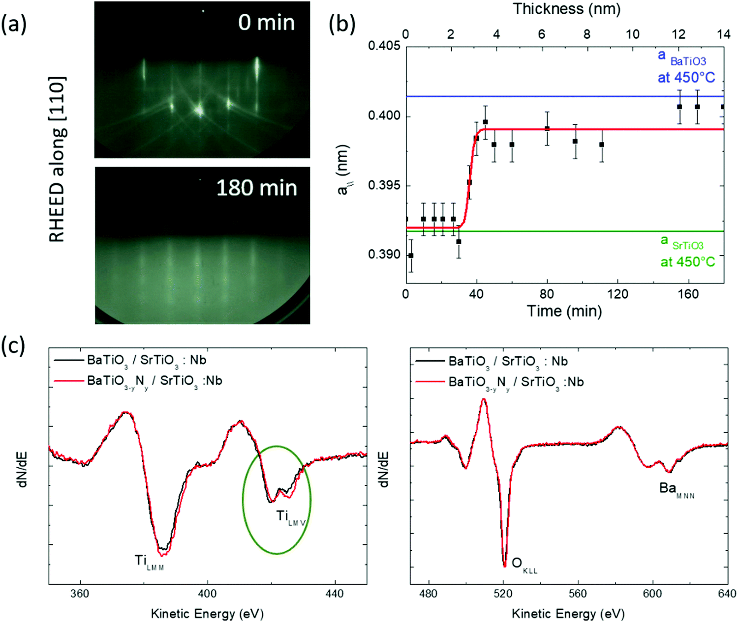 | ||
| Fig. 1 (a) Typical RHEED patterns, along [110] azimuths, observed during the growth of N:BTO/Nb:STO. The total thickness is 14 nm after 180 min of deposition. (b) Evolution of the N:BTO/Nb:STO in-plane lattice parameter (denoted by a//) derived from RHEED patterns recorded during growth at a sample temperature of 450 °C. Horizontal green and blue lines indicate the SrTiO3 and BaTiO3 bulk cubic lattice parameters at 450 °C. (c) Auger scans for BTO and N:BTO layers deposited on Nb:STO (350 eV to 450 eV and 470 eV to 640 eV). | ||
Further investigations were performed using AES. The AES spectra recorded after growth are reported in Fig. 1b for doped and undoped samples. The spectra are very similar. The uncorrected TiLMM/BaMNN ratio is 1.3, which is close to the expected value for a 1:1 stoichiometry for Ti:Ba as it was reported in the literature.7,17 A closer inspection of the Auger spectra shows that the TiLMV peak presents two components with slightly different relative intensities, which were widely used to determine changes in the stoichiometry of Ti compound surfaces, as well as variations in the surface oxygen stoichiometry after metal deposition.18 Rao et al.19 considered the evolution of the TiL2,3M2,3V Auger spectra through a series of compounds presenting a gradual reduction of the titanium ion from TiO2 to metallic titanium. The spectrum evolves from a unique line around a kinetic energy of 408 eV in TiO2, to a unique line at around 414 eV in metallic titanium. By convention, when the metal is oxidized, the low kinetic energy component has been assigned to a so called “interatomic L3MV(O)” decay, while the other (metallic) component has been associated with an “intra-atomic L3MV(Ti)” process20,21 where V(O) and V(Ti) refer to O and Ti contributions to the oxide valence band, respectively. One observes in Fig. 1(c) that the first component is reduced in the N doped sample suggesting less oxidized Ti species in this sample. Importantly, such a modification of the electronic structure suggests an incorporation of the N atoms in the lattice of the material and/or oxygen vacancies.
The crystalline structure of the N:BTO layers was investigated by X-ray diffraction (XRD) and X-ray reflectivity (XRR). Fig. 2a shows the reflectivity curve as a function of the wave vector transfer Qz, measured on the N:BTO film as well as the calculated reflectivity for the best fit model (straight line) refined using the REFLEX software.22 While a single layer model failed to represent the data, a simple 2-layer model allowed the reproduction of experimental measurement very well (χ2 = 0.007). The best fit gives a homogeneous layer of thickness 12 nm covered by a surface layer of 2 nm with a lower density. The inset in Fig. 2a reproduces the density profile of the best fit model. The substrate roughness was 0.27 nm r.m.s. and the top layer roughness was of ca. 0.33 nm r.m.s. Given the growth method, the sharp layer model obtained here is a striking feature.
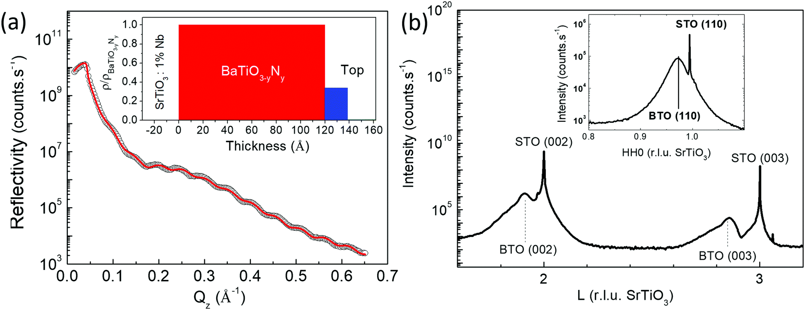 | ||
| Fig. 2 (a) Specular reflectivity measurements (°) and best fit (–) for the N:BTO sample deposited on SrTiO3:1% Nb. The inset shows the density profile corresponding to the best fit. (b) Wide angle X-ray diffraction along specular direction for N:BTO sample. (inset) In surface plane scan along the [HH0] direction across the 110 Bragg peaks of N:BTO and Nb:STO. | ||
Fig. 2b shows the wide angle XRD patterns of the N:BTO sample. All Bragg peaks could be well fitted using Lorentzian shaped peaks. The widths of the diffraction peaks of SrTiO3(001) are limited by the instrumental contribution and are thus very sharp and point out the high crystalline quality of the single crystalline substrate. The specular Bragg peaks of N:BTO appear in the form of broad peaks on the low L side of the Nb:SrTiO3 Bragg peaks and contain information about the film thickness and strain.23–26 Epitaxial single crystalline films only exhibit a single family of Bragg peaks along [00L] limiting the number of peaks that can be taken into account in a structural size–strain nanoparticle analysis.27 The peak widths and positions were determined and reported in the corresponding Scherrer plot (refer to Fig. S1 in the ESI†), which leads to an average particle size of (10.1 ± 2.7) nm which is essentially close to the film thickness. Thus, the widths of the specular peaks are dominated by the finite film thickness preventing the extraction of information about the strain in the layer. Indeed, broad peaks in the perpendicular reciprocal space are intrinsically expected for films of reduced real space thickness. Rocking scans, measured for all accessible specular Bragg peaks, revealed very narrow peaks (∼0.022°) limited by the experimental resolution stressing the high crystalline quality of the layer. The film exhibited also well-defined in-plane Bragg peaks (Fig. 2b inset) accessible in grazing incidence geometry, i.e. at an incidence angle of 0.5°, which is close to two times the critical angle for total external reflection at the measurement photon energy. In surface plane rocking scans were performed on all accessible peak positions. The in-plane Bragg peaks widths (full widths at half maximum, FWHM), Δ, decrease steadily with increasing momentum transfers. They are indeed expected to follow equation Δ2 = Ω2 + (2π/(Q × D))2, where Ω is the in-plane mosaic spread (i.e. a constant angular width), and D a finite domain size, which leads to a constant broadening with respect to the momentum transfer, Q, and is related to the angular width Δω by D = 2π/(Q × Δω). Both values can be easily retrieved from the linear fit to the Δ2 = f(1/Q2) plot (refer to Fig. S2 in the ESI†).28 For our layer we obtain a mosaic spread as small as 1.27° and a domain size of 7 nm, confirming the epitaxial single crystalline nature of the layer. The lattice parameters were determined from the averaged Bragg peak positions and were a = (0.398 ± 0.001) nm and c = (0.408 ± 0.003) nm. As is illustrated in Table 1, the doped layer is significantly more tetragonal (c/a = 1.025) than the undoped one (c/a = 1.010).7 This difference may find its explanation in the substitution of oxygen by nitrogen atoms in the lattice due to the charge imbalance and an increased presence of vacancies. Also for AES, these results suggest that N has been incorporated in the lattice of the N:BTO layer.
| Sample | a (nm) | c (nm) | c/a | Electrochemical band gap (eV) |
|---|---|---|---|---|
| BaTiO3 | 0.399 | 0.403 | 1.01 | 3.62 ± 0.01 |
| BaTiO3−yNy | 0.398 | 0.408 | 1.025 | 3.61 ± 0.01 |
The electronic structure of our N:BTO layer was examined by XPS measurements and compared with that of the well documented BTO case.29–36 The main photoemission peaks are represented in Fig. 3 for doped and undoped samples. Both samples showed a main O-1s line at 529 eV binding energy (refer to Fig. S3 in the ESI†). While this line cannot be quantitatively interpreted because of the air exposure, its overall shape remains of interest to evidence the presence of a well marked contribution at lower binding energy. The main O-1s line positions were found to be symmetric, which indicate a well defined single electronic state for the oxygen atoms incorporated into the oxide structure. With respect to Ti-2p the intensity of the integrated O-1s XPS peak is 1.8% lower for the N-doped BaTiO3 layer which is consistent with the partial substitution of O by N. The N-doped film displayed a N-1s XPS peak (Fig. 3b), which can be decomposed into two components. The peak observed at binding energy 398.3 eV can be ascribed to Ti–O–N bonds or surface adsorbed nitrogen while the peak located at 395.5 eV can be assigned to Ti–N bonds.37 The composition of the sample was determined from XPS data using the CasaXPS software. It allows establishing the N/Ti and N/Ba ratios of 3.8% and 2.9%, respectively, which correspond to a N/O ratio of ca. 1% which is a rather remarkably high value for a perovskite lattice built without charge compensating cations. The Ti-2p3/2 line shows a narrow single feature located at 457.8 eV binding energy for the undoped sample which is slightly shifted to 457.6 eV for the N-doped one (Fig. 3a). A similar shift of about ∼0.2 eV was reported by Wang et al.38 in a N doped SrTiO3 sample. Since the electronegativity of N is smaller than that of O, after the incorporation of nitrogen the electron density increases on Ti. This mechanism may explain the energy shift. Importantly, the Ti-2p line cannot be decomposed into several components for the doped sample indicating that Ti atoms adopt a well defined oxidation state, as expected for a homogeneous material.
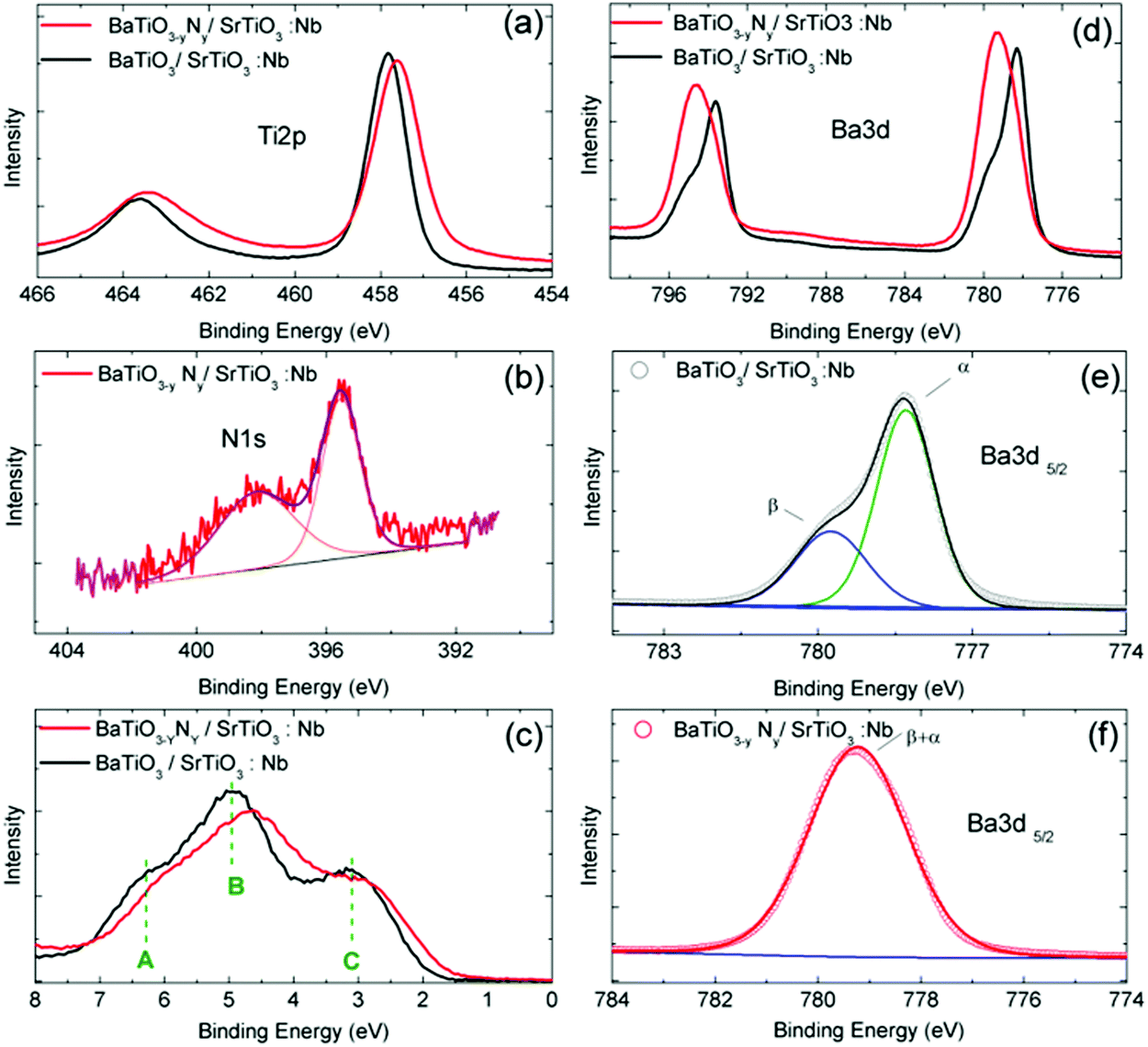 | ||
| Fig. 3 Photoemission spectra of undoped (black) and N-doped (red) BaTiO3 layers for (a) Ti-2p, (b) N-1s core levels, (c) the valence band region, (d) Ba-3d, (e) Ba 3d5/2 (undoped), the green contribution corresponds to the α component and the blue one to the β component, and (f) Ba 3d5/2 (doped). For (e and f) symbols stand for experimental data. For (b, e and f) thin bottom lines correspond to Shirley type backgrounds and thick straight lines to best fits. The best-fit parameters are reported in Table 2. | ||
The valence band (VB) region measured shows also modifications upon doping (Fig. 3d). The valence band of the N-doped sample is shifted by 0.2 eV towards lower binding energies, as was predicted by Zou et al. in N doped SrTiO3.39 The resulting shift stresses the presence of vacancies in the film.40 The shape of the valence band of BTO has been studied in detail in previous reports and consists of 3 well defined contributions (labelled A, B, and C in Fig. 3c). It was shown that it is composed of a pure O-2p π contribution for the low energy part and O-2p σ hybridized with Ti-3d levels for the high-energy contributions. This fine structure is modified for the doped sample. These modifications of the valence band shape can be related to changes in the crystallographic structure and in hybridization between Ti and O orbitals.
For the undoped film, the decomposition in individual lines of the Ba-3d5/2 peak reveals the presence of two components. They have been associated with two different chemical states already in early studies41 of BaTiO3 surfaces and are usually labeled α and β (Fig. 3e and f). The best fit parameters of the decomposition in individual lines are reported in Table 2. Already in the pioneering work of Mukhopadhyay et al.,41 the α component was attributed to the bulk perovskite phase and the β component to a more surface like environment. More recent studies7 demonstrated that the surface layer was likely made of Ba oxides that can be removed by ethanol etching. This interpretation was finally refined recently in two studies42,43 concluding that the β component is likely associated more precisely with a surface Ba peroxide (BaO2) layer. For the N-doped BaTiO3 film, the Ba-3d5/2 peak shows a broad single component at an intermediate position between α and β components. The chemical environment of Ba is thus strongly modified by the presence of N in the lattice. Another difference induced by N doping can be seen in the overview XPS spectrum (refer to Fig. S4, ESI†). One observes that N doping completely prevents the segregation of Sr in the film. Residual Sr is often observed in thin films grown with atomic oxygen plasma due to easy substitution between Ba and Sr in the perovskite lattice.
:Nb samples. EB stands for binding energy, Δ for peak width (full width at half maximum values), and ρ for the relative weight of each line
| Ba 3d3/2 | Ba 3d5/2 | ||||||
|---|---|---|---|---|---|---|---|
| Peak | EB (eV) | Δ (eV) | ρ (%) | EB (eV) | Δ (eV) | ρ (%) | |
| BTO | |||||||
| α | 793.6 | 1.39 | 28.5 | 778.3 | 1.34 | 40.0 | |
| β | 795.1 | 1.52 | 12.1 | 779.7 | 1.68 | 19.3 | |
| N:BTO |
|||||||
| α + β | 794.5 | 2.23 | 39.78 | 779.2 | 2.25 | 59.2 | |
Oxynitride films show promise to be used as photoanodes in the framework of solar water splitting. The photocurrent measurements on BTO and N:BTO samples are shown in Fig. 4a and the PEC response is completely different from the response of a bare Nb:SrTiO3 substrate (refer to Fig. S5, ESI†). The change in magnitude and shape of the photoresponse of the films with respect to the bare substrate demonstrates that the measurements performed on films are not mingled with the signal coming from the substrate. We observe a slight improvement of the PEC properties upon N-doping, for example, at 0 V vs. Ag/AgCl, the photocurrent density (Jph) increases from 17 μA cm−2 for the undoped sample up to 19 μA cm−2 for the doped one. This difference increases with voltage and at 0.7 V vs. Ag/AgCl, the photocurrent generated in the doped sample is 63% larger than for the undoped one. This observation is consistent with the results of Xing et al.40 who reported an improvement of the PEC properties with N doping of SrTiO3 prepared by the hydrothermal method. These authors concluded that nitrogen doping not only modulates the visible light absorption feature, but also has consequences on the enhancement of charge separation efficiency, which can promote the photocatalytic activity. Although, according to their results, it was hard to give a solid conclusion about which parameter among the doping level, the crystallinity or nano-structuring was the major factor contributing to the improvements in the PEC properties.
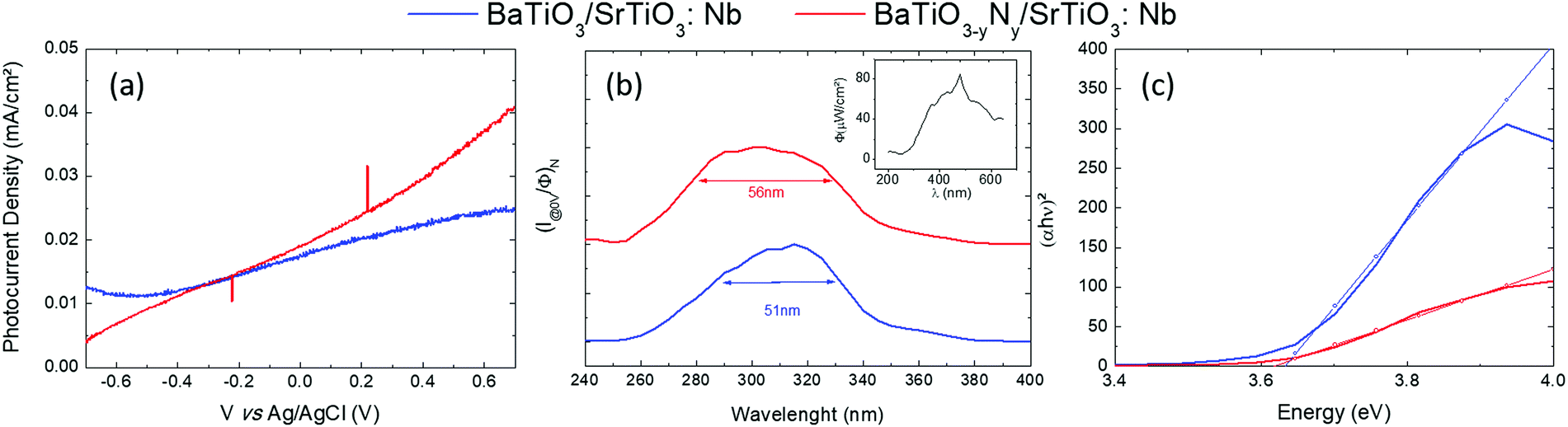 | ||
| Fig. 4 (a) Photocurrent density versus the applied voltage (vs. Ag/AgCl), (b) efficient absorption photocurrent density as a function of the wavelength at 0 V vs. Ag/AgCl, (inset) light flux of the Xe arc lamp as a function of the wavelength, (c) direct band gaps determined using the “efficient Tauc plot method”, for undoped (blue) and N-doped (red) BaTiO3 layers. | ||
To get insight into the spectral response of our layers we have performed photocurrent measurements as a function of the incident light wavelength. The photocurrent density data normalized to the corresponding incident light flux are reported in Fig. 4b. The Full Width at Half Maximum (FWHM) of spectral absorption is 51 nm and 54 nm for BTO and N:BTO respectively. The window of “efficient absorption” is much larger for the N-doped sample and its maximum is slightly shifted towards the Ultra-Violet (UV) light range within a nearly symmetric shape, as compared to the other situations. We estimated (Fig. 4c) the photoelectrochemical band gaps of our samples through the “efficient Tauc plot” method,44 by plotting (αhν)2vs. hν (hν being the photon energy and α the absorption coefficient of the material). The photoelectrochemical band gaps determined in this way are 3.62 eV and 3.61 eV for undoped and N-doped samples respectively. These values are very close to the band gap value from the literature for BaTiO3 (3.7 eV). When doping an n-type material, the band gap can increase or decrease. With a Fermi level near the conduction band edge, the charge carrier concentration of n-type semiconductors will increase when doped with electron donor atoms. If the Fermi level moves into the conduction band (Burstein Moss shift), the apparent band gap will increase as has been reported for various materials including non-oxide films,45 oxide nanostructured films,46 non-oxide nanosheets47 and oxide films.48 However, if electronic states are created just above the valence band, the apparent bandgap will decrease. The slight reduction of the band gap and the increase in the efficient absorption window observed in the present study are consistent with the results reported by Xing et al.40 on N doped SrTiO3. They claimed that oxygen vacancies positively shift the conduction band minimum while, to the contrary, N-doping tends to shift negatively the valence band maximum, leading thus to a reduction of the band gap value.
Discussion
In this work, we managed to grow an epitaxial oxynitride thin film of N:BTO by a genuine approach. The film containing about 3.8% N (with respect to Ti) was grown using an atomic N plasma source under equivalent conditions to the ones used for an atomic oxygen plasma that allows the growth of epitaxial BaTiO3(001) on SrTiO3(001) substrates. Rather than leading to a nitride film that one could naively expect, we observe a self-doped low N concentration oxynitride film. This behavior indicates necessarily a cooperative self-diffusion of O coming from the SrTiO3 substrate and a self-limitation of the N content. The limiting factor is likely linked to our growth conditions (as e.g. sample temperature and metal fluxes). The film is homogeneous with a number of striking properties. The well-contrasted RHEED patterns show that the layer is single crystalline and epitaxial with a simple cube/cube epitaxial relationship. It is of 2D nature up to 8 nm before faint additional 3D features appear. The lattice parameter relaxation occurs during the first few nanometers and is almost completed at 12 nm. The lattice parameters of pure BaTiO3 and N : BaTiO3 samples are listed in Table 1. We note that, compared to an equivalent BTO film, the a lattice parameter of the N:BaTiO3 layer is smaller by 0.001 nm and its c parameter is larger by 0.005 nm leaving the perovskite structure far more tetragonal than pure BaTiO3. This may be better understood in the light of the photoemission results showing that the N atoms are incorporated in the material lattice and that a higher oxygen vacancy level is likely to ensure charge neutrality. Both of these effects can explain the larger c/a value. The fact that nitrogen occupies the oxygen sites in the BaTiO3 host matrix may result in lattice expansion because the ionic radius of N3− is 0.146 nm, which is slightly larger than the 0.138 nm of O2−. An increase of c/a is expected for BTO layers having higher O vacancy contents.49–51 The underlying mechanisms may be linked to the recently reported oxygen diffusion52 that is expected in BaTiO3 and SrTiO3 having oxygen vacancies. For a given level of oxygen vacancies, the activation energy of oxygen diffusion is found to be smaller for SrTiO3 than for BaTiO3 and strongly decreases for increasing levels of vacancies. Both these features favour migration of oxygen atoms from SrTiO3 to BaTiO3, especially of oxygen deficient thin films. Importantly, the substitution of O by N in the BTO lattice profoundly modifies the electronic structure leading to an enhanced active spectral optical absorption window, a behaviour that leads to enhanced PEC performance, up to 63% at 0.7 V. The improvement of PEC performance observed here might be due to (i) better light absorption, (ii) better kinetics at the electrode/electrolyte interface and/or (iii) a lower recombination rate. We measured a narrower band gap but the difference between both samples remains small and may not solely explain the 63% improvement. Moreover, no change in the transient photocurrent could be observed during the ON/OFF photocurrent measurements (refer to Fig. S5, ESI†), showing that the kinetics at the interface remains unchanged. However, we have shown that oxygen vacancies as well as N doping add charge carriers in the sample likely to modify the electronic structure. Therefore, we can expect a higher conductivity inside the sample, upon doping, inducing a reduction of the recombination rate. The larger c/a ratio may also influence the photocurrent since higher tetragonality (i.e. larger c/a values) also implies a larger ferroelectric polarization, which can also strongly influence the generated photocurrent depending on its orientation.11
Conclusions
In summary, we have demonstrated that atomic nitrogen assisted molecular beam epitaxy is a suitable technique to fabricate homogeneous epitaxial N-doped (3.8% with respect to Ti) BaTiO3 by taking advantage of the diffusion of O from the SrTiO3 substrate into the film. All experimental observations are consistent with N substitution of O in the perovskite lattice. The N self-doping is believed to be self-limited by the concomitant need for the incorporation of O vacancies ensuring charge neutrality. This original method allows the growth of oxynitride films of very high crystalline quality otherwise very challenging to realize. The incorporated N atoms homogenously modify the electronic structure and enlarge the spectral light absorption of this new class of materials that shows promise for usage as improved light harvesting materials.Author contributions
Films were made by A. D and A. B as well as the RHEED and the AES spectroscopy. XRD and XRR diffraction measurements were performed by C. M. J. L. performed XPS. The PEC analysis was conducted by A. D and H. M. The XPS measurements were realized by A. D. H. M. A. B. and P. F. The project was led by A. B and the paper was written by A. D. with contributions from all authors. All authors have given approval to the final version of the manuscript.Conflicts of interest
There are no conflicts to declare.Acknowledgements
This work received support from a public grant overseen by the French Research Agency (ANR) as part of the “Investissement d’Avenir” program (LABEX NanoSaclay, ref ANR-10-LABX-0035) through the project “DOPNOXBV”. It was also funded by the CEA (Focus-FCC program under the OXYNITRODE grant). We acknowledge SOLEIL Synchrotron for provision of synchrotron radiation facilities and are grateful for assistance while using the DiffAbs and CASSIOPEE beamlines.Notes and references
- A. Fujishima and K. Honda, Nature, 1972, 238, 37 CrossRef CAS PubMed.
- M. Grätzel, Nature, 2001, 414, 338 CrossRef PubMed.
- M. G. Walter, E. L. Warren, J. R. McKone, S. W. Boettcher, Q. Mi, E. A. Santori and N. S. Lewis, Chem. Rev., 2010, 110, 6446 CrossRef CAS PubMed.
- R. van de Kroel, Y. Liang and J. Schooman, J. Mater. Chem., 2008, 18, 2311 RSC.
- J. Pan, J. Phys. Chem. Lett., 2015, 6, 5027 CrossRef CAS PubMed.
- A. Zakutayev, J. Mater. Chem., 2016, 18, 6742 RSC.
- A. Barbier, C. Mocuta, D. Stanescu, P. Jegou, N. Jedrecy and H. Magnan, J. Appl. Phys., 2012, 112, 114116 CrossRef.
- K. J. Choi, M. Biegalski, Y. L. Li, A. Sharan, J. Schubert, R. Uecker, P. Reiche, Y. B. Chen, X. Q. Pan, V. Gopalan, L. Q. Chen, D. G. Schlom and C. B. Eom, Science, 2004, 306, 1005 CrossRef CAS PubMed.
- D. Stanescu, H. Magnan, B. Sarpi, M. Rioult, T. Aghavnian, J. Moussy, C. Rountree and A. Barbier, ACS Appl. Nano Mater., 2019, 6, 3556 CrossRef.
- M. Rioult, S. Datta, D. Stanescu, S. Stanescu, R. Belkhou, F. Maccherozzi, H. Magnan and A. Barbier, Appl. Phys. Lett., 2015, 107, 103901 CrossRef.
- H. Magnan, P. M. Deleuze, J. Brehin, T. Plays, D. Stanescu, W. R. Flavell, M. G. Silly, B. Domenichini and A. Barbier, J. Phys. Chem. C, 2020, 124, 10315 CrossRef CAS.
- D. Wang, L. Jia, X. Wu, L. Lu and A. Xu, Nanoscale, 2012, 4, 576 RSC.
- J. Cao, Y. Ji, C. Tian and Z. Yi, J. Alloys Compd., 2014, 615, 243 CrossRef CAS.
- D. Fang, F. He, J. Xie and L. Xue, J. Wuhan Univ. Technol., Mater. Sci. Ed., 2020, 35, 711 CrossRef CAS.
- N. Fairley, V. Fernandez, M. Richard-Plouet, C. Guillot-Deudon, J. Walton, E. Smith, D. Flahaut, M. Greiner, M. Biesinger, S. Tougaard, D. Morgan and J. Baltrusaitis, Appl. Surf. Sci. Adv., 2021, 5, 100112 CrossRef.
- H. Magnan, D. Stanescu, M. Rioult, E. Fonda and A. Barbier, J. Phys. Chem. C, 2019, 123, 5240 CrossRef CAS.
- K. Shimoyama, K. Kubo, T. Maeda and K. Yamabe, J. Appl. Phys., 2001, 40, L463 CrossRef CAS.
- P. Le Fevre, J. Danger, H. Magnan, D. Chandesris, J. Jupille, S. Bourgeois, M. A. Arrio, R. Gotter, A. Verdini and A. Morgante, Phys. Rev. B: Condens. Matter Mater. Phys., 2004, 69, 155421 CrossRef.
- C. N. Rao and D. D. Sarma, Phys. Rev. B: Condens. Matter Mater. Phys., 1982, 25, 2927 CrossRef CAS.
- W. Göpel, J. A. Anderson, D. Frankel, M. Jaehnig, K. Phillips, J. A. Schaefer and G. Rocker, Surf. Sci., 1984, 139, 333 CrossRef.
- H. R. Sadeghi and V. E. Henrich, J. Catal., 1988, 109, 1 CrossRef CAS.
- A. Gibaud and G. Vignaud, Specular Reflectivity from Smooth and Rough Surfaces. In: Daillant J., Gibaud A. (eds) X-ray and Neutron Reflectivity. Lecture Notes in Physics, Published bySpringer, Berlin, Heidelberg, 2009, vol. 770, ch. 3, pp. 85-131 Search PubMed.
- T. Tsurumi, S. Nishizawa and N. Ohashi, Jpn. J. Appl. Phys., 1999, 38, 3682 CrossRef CAS.
- J. N. Zeng, J. K. Low, Z. M. ren, T. Liew and Y. F. Lu, Appl. Suf. Sci., 2002, 197, 362 CrossRef.
- T. Ishibe, Y. Maeda, T. Terada, N. Naruse, Y. Mera, E. Kobayashi and Y. Nakamura, Sci. Technol. Adv. Mater., 2020, 21, 195 CrossRef CAS PubMed.
- M.-J. Zhao, Z.-T. Sun, Z.-X. Zhang, X.-P. Geng, W.-Y. Wu, S.-Y. Lien and W.-Z. Zhu, Materials, 2020, 13, 3910 CrossRef CAS PubMed.
- D. Nath, F. Singh and R. Das, Mater. Chem. Phys., 2020, 239, 122021 CrossRef CAS.
- A. Barbier, C. Mocuta and G. Renaud, Handbook of Thin Films, ed. H. S. Nalwa, In situ synchrotron structural studies of the growth of oxides and metals, Published by Academic Press, 2001, vol. 2, ch. 11, pp. 527–596 Search PubMed.
- Y. Adachi and S. Kohiki, Appl. Phys. Lett., 1988, 84, 4 Search PubMed.
- D. Ehre, H. Cohen, V. Lyahovitskaya and I. Lubomirsky, Phys. Rev. B: Condens. Matter Mater. Phys., 2008, 77, 184106 CrossRef.
- L. T. Hudson, R. L. Kurtz, S. W. Robey, D. Temple and R. L. Stockbauer, Phys. Rev. B: Condens. Matter Mater. Phys., 1993, 47, 1174 CrossRef CAS PubMed.
- S. B. Zhang, Phys. Rev. B: Condens. Matter Mater. Phys., 1999, 60, 4462 CrossRef CAS.
- J. Kano, N. Ikeda, T. Teranishi, T. Fujii, T. Ueda and T. Ohkubo, J. Appl. Phys., 1993, 120, 154101 Search PubMed.
- J. J. Ritsko, A. J. Epstein, W. R. Salaneck and D. J. Sandman, Phys. Rev. B: Condens. Matter Mater. Phys., 1978, 17, 1506 CrossRef CAS.
- E. Wachtel and I. Lubomirsky, Adv. Mater., 2010, 22, 2485 CrossRef CAS PubMed.
- J. L. Wang, A. Pancotti, P. Jégou, G. Niu, B. Gautier, Y. Y. Mi, L. Tortech, S. Yin, B. Vilquin and N. Barrett, Phys. Rev. B: Condens. Matter Mater. Phys., 2011, 84, 205426 CrossRef.
- A. Trenczek-Zajac, M. Radeckaa, K. Zakrzewska, A. Brudnik, E. Kusior, S. Bourgeois, M. C. Marco de Lucas and L. Imhoff, J. Power Sources, 2009, 194, 93 CrossRef CAS.
- D. Wang, L. Jia, X. Wu, L. Lu and A. Xu, Nanoscale, 2012, 4, 576 RSC.
- F. Zou, Z. Jiang, X. Qin, Y. Zhao, L. Jiang, J. Zhi, T. Xiao and P. Edwards, Chem. Commun., 2012, 48, 8514 RSC.
- G. Xing, L. Zhao, T. Sun, Y. Su and X. Wang, SpringerPlus, 2016, 5, 1132 CrossRef PubMed.
- S. M. Mukhopadhyay and T. C. S. Chen, J. Mater. Res., 1995, 10, 1502 CrossRef CAS.
- S. Chakrabarti, S. Ginnaram, S. Jana, Z. Y. Wu, K. Singh, A. Roy, P. Kumar, S. Maikap, J.-T. Qiu, H.-M. Cheng, L.-N. Tsai, Y.-L. Chang, R. Mahapatra and J.-R. Yang, Sci. Rep., 2017, 7, 4735 CrossRef PubMed.
- T. C. Droubay, L. Kong, S. A. Chambers and H. P. Hess, Surf. Sci., 2015, 632, 201 CrossRef CAS.
- J. Tauc, Mater. Res. Bull., 1968, 3, 37 CrossRef CAS.
- M. P. Polak, P. Scharoch and R. Kudrawiec, J. Phys. D: Appl. Phys., 2017, 50, 195103 CrossRef.
- T. Ishibe, A. Tomeka, K. Watanabe, Y. Kamakura, N. Mori, N. Naruse, Y. Mera, Y. Yamashita and Y. Nakamura, ACS Appl. Mater. Interfaces, 2018, 10, 43 CrossRef PubMed.
- S. Muthu Mariappan, M. Shkir, T. Alshahrani, V. Elangovan, H. Algarni and S. Alfaigy, J. Alloys Compd., 2021, 859, 157762 CrossRef.
- A. Tomeda, T. Ishibe, T. Tanigushi, R. Okuhata, K. Watanabe and Y. Nakamura, Thin Solid Films, 2018, 666, 185 CrossRef CAS.
- C. Li, Z. Chen, Y. Zhou and D. Cui, J. Phys.: Condens. Matter, 2001, 13, 5261 CrossRef CAS.
- T. Zhao, F. Chen, H. Lu, G. Yang and Z. Chen, J. Appl. Phys., 2000, 87, 7442 CrossRef CAS.
- A. Chen, F. Khatkhatay, W. Zhang, C. Jacob, L. Jiao and H. Wang, J. Appl. Phys., 2013, 114, 124101 CrossRef.
- J. Dawson, Phys. Status Solidi B, 2020, 257, 1900422 CrossRef CAS.
Footnote |
| † Electronic supplementary information (ESI) available. See DOI: 10.1039/d1ma01082d |
| This journal is © The Royal Society of Chemistry 2022 |