
 Open Access Article
 This Open Access Article is licensed under a
 Creative Commons Attribution 3.0 Unported Licence
Fabrication of solution-processable OFET memory using a nano-floating gate based on a phthalocyanine-cored star-shaped polymer†
Junko
Aimi
 *a,
Takeshi
Yasuda
a,
Chih-Feng
Huang
b,
Masafumi
Yoshio
a and
Wen-Chang
Chen
c
*a,
Takeshi
Yasuda
a,
Chih-Feng
Huang
b,
Masafumi
Yoshio
a and
Wen-Chang
Chen
c
aResearch Center for Functional Materials, National Institute for Materials Science (NIMS), 1-2-1 Sengen, Tsukuba, Ibaraki 305-0047, Japan. E-mail: AIMI.Junko@nims.go.jp
bDepartment of Chemical Engineering, i-Center for Advanced Science and Technology (iCAST), National Chung Hsing University, Taichung 40227, Taiwan
cDepartment of Chemical Engineering, National Taiwan University, Taipei 10617, Taiwan
First published on 4th February 2022
Abstract
Solution-processed organic field-effect transistor (OFET) memory devices are fabricated using a blend film of 6,13-bis(triisopropylsilylethynyl)pentacene and phthalocyanine-cored star-shaped polystyrene. A highly crystalline organic semiconductor thin film was obtained on the star-shaped polymer with charge-trapping sites via a one-pot spin-coating process through vertical phase separation, which is advantageous for OFET memory device applications. The resultant OFET device demonstrated a charge carrier mobility of 0.10 cm2 V−1 s−1 and an on/off current ratio of 106. Upon application of a gate bias, a substantial reversible threshold shift was observed, along with long charge-retention ability, thereby confirming the memory characteristics of the device.
Introduction
Nonvolatile organic field-effect transistor (OFET) memory devices have attracted much attention because of their easily integrated structure and nondestructive readout.1,2 They are regarded as a promising technology to integrate switching capacity and memory into various organic electronic devices such as sensors, displays, and radio-frequency identification tags. Meeting the recent demand for flexible, wearable, and large-area electronic devices via an easy and low-cost production process will necessitate the development of solution-processable OFET memories.3–5 However, OFET memory often requires complicated and multistep fabrication processes because it contains multilayers of thin films, including an organic semiconductor for charge transport and a memory layer for charge trapping as well as a tunneling layer for charge insertion/extraction and a blocking layer for charge retention.6–8 In addition, the active layer of an organic semiconductor in OFET memory devices is normally prepared by vacuum deposition to achieve high charge carrier mobility. Therefore, the preparation of OFET memory devices using simple solution processes is a key challenge.9–14Solution-processable organic semiconductors themselves have been extensively investigated and incorporated into OFET devices. For instance, 6,13-bis(triisopropylsilylethynyl)pentacene (TIPS-pentacene) is a typical small-molecule semiconductor with solubilizing side groups. The charge-carrier mobility in OFET devices is strongly influenced by the crystalline structure and alignment of the organic semiconductors.15 To achieve high device performance using a solution process, researchers have studied various methods of preparing thin films of organic semiconductors. Polymer-matrix-assisted phase separation is one of the most promising methods to prepare OFETs with high charge carrier mobility.16–21 The mixed polymer increases the wettability of the substrates and decreases the evaporation speed of the solvents to induce crystallization of the organic semiconductor. For instance, an OFET prepared using a spin-coated blend film of TIPS-pentacene and poly(α-methylstyrene) exhibited a charge carrier mobility as high as 0.54 cm2 V−1 s−1.17 The selection of an appropriate polymer insulator,22–24 polymer molecular weight,17,25,26 and processing solvent27–30 is important for controlling the crystal growth of organic semiconductors in the polymer matrix. Further advances in the coating process, such as the development of the blade coating technique,25,31,32 have led to additional enhancements in OFET device performance.
Here we envision that the method of using a polymer matrix to construct high-performance OFET devices via a solution process can also be applied to OFET memory devices when the matrix polymer is capable of charge storage. Recently, we prepared metallophthalocyanine (MPc)-cored star-shaped polystyrene (MSP) and used it as a charge-trapping material in a pentacene-based OFET memory device.33 The star polymer with an MPc core is readily soluble in organic solvents, enabling the fabrication of polymer films with a smooth surface via simple spin-coating onto a Si substrate. The MSP films exhibited a unique three-dimensional morphology, where the MPc cores were distributed and isolated by the surrounding arm-polymer matrix. A bottom-gate top-contact OFET memory device was fabricated via vacuum deposition of pentacene onto the polymer film, followed by deposition of Au electrodes. When a negative gate voltage was applied to the device, hole charges that accumulated in pentacene migrated to the MPc core, whereas polystyrene arms restrained leakage of the trapped charges to achieve nonvolatile memory similar to that based on nano-floating-gate transistors. In addition, the density of the MPc core—specifically, charge-trapping sites, can be controlled by the length of the arm polymer, enabling control of the resultant memory device performance.34
As a continuation of our studies on the OFET memory devices, we herein attempt to develop a simple and easy method of preparing OFET memory devices using polystyrene-based nano-floating gates. We used our unique design of memory materials—star-shaped polystyrene with specific charge-trapping sites—to prepare vertically phase-separated organic semiconductor/memory layers via a one-pot solution process. More specifically, the MPc-cored star-shaped polystyrene promotes the crystallization of small molecular semiconductors of TIPS-pentacene via polymer-matrix-assisted phase-separation and simultaneously provides organic semiconductor/memory layers on the substrates. The morphology and structure of the blend films of the star polymer and TIPS-pentacene prepared by a simple spin-coating process from various organic solvents were investigated using X-ray diffraction (XRD), atomic force microscopy (AFM), polarized optical microscopy, UV-vis absorption spectroscopy, and X-ray photoelectron spectroscopy (XPS). We obtained highly crystalline and vertically phase-separated TIPS-pentacene on star polymer blend films from an ortho-dichlorobenzene (ODCB) solution, which is advantageous for OFET memory device applications. We finally demonstrated an OFET device with a bottom-gate top-contact configuration (Fig. 1a). The resultant device showed a hole mobility of 0.1 cm2 V−1 s−1 and a high on/off current ratio greater than 106. In addition, a memory window of 19.7 V was probed under an applied gate voltage in the range ±50 V and the device demonstrated long charge-retention ability. Thus, the present one-pot solution process would be a useful approach for preparing non-volatile organic memories without cumbersome fabrication and costly vacuum-deposition processes of organic semiconductors.
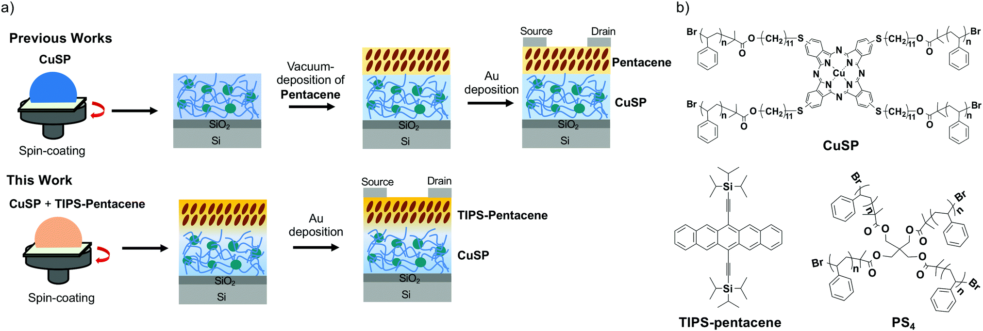 | ||
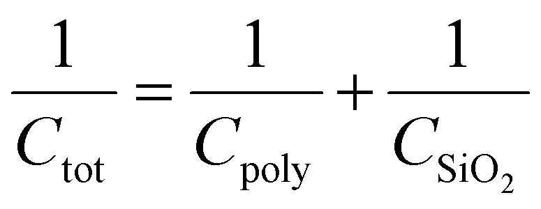
| Fig. 1 (a) Schematic representation of the fabrication of OFET memory devices. (b) Chemical structures of TIPS-pentacene and polymer dielectrics of CuSP and PS4. | ||
Experimental
Materials and methods
Commercial chemicals, which were purchased from Sigma-Aldrich, TCI, Wako Chemicals, or Kanto Chemicals, were used without further purification unless noted otherwise. All reactions were conducted under Ar in oven-dried glassware.Measurements
Electronic absorption spectra were recorded on a JASCO V-670 spectrophotometer. X-Ray diffraction (XRD) measurements were carried out using a Rigaku MiniFlex 600 (Ni-filtered Cu K radiation, Rigaku, Tokyo, Japan). X-Ray photoelectron spectroscopy (XPS) was performed using a PHI Quantera SXM (ULVAC-PHI, Japan) with a monochromatic Al Kα X-ray source. Atomic force microscopy (AFM) was performed under ambient conditions with a Bruker MultiMode 8 atomic force microscope. Imaging was conducted in the ScanAsyst mode using a silicon cantilever (NCHV-A) with a frequency of 270–400 kHz. The optical texture of the organic semiconductor crystals was analyzed by polarizing optical microscope (Olympus BX51N-31P-O3, Olympus, Tokyo, Japan), equipped with a DP22 digital camera.Device measurements
The film thickness of each layer was measured using a microfigure measuring instrument (SURFCORDER ET200; Kosaka Laboratory, Tokyo). Devices were fabricated on highly doped n-type Si(100) wafers with a 300 nm-thick SiO2 layer. In this study, all of the results for memory performance were averaged from at least ten devices from five batches. All measurements on the transistor memory devices were conducted with a Keithley 2636B source measurement unit under dark ambient conditions. Triaxial cables were connected to the probe station to minimize background noise. The effective charge carrier mobility (μeff) and threshold voltage (Vth) values were estimated from the slope and intercept of the linear plot of the square root of the drain-to-source current (Ids1/2) vs. the gate voltage (Vg) in the saturation regime using the following equation:| Ids = WCtotμeff(Vg − Vt)2/(2L) | (1) |
The relations between the capacitance (Ctot) of the device, SiO2 wafer (CSiO2), polymers (Cpoly), and polymer dielectric constant (ε) are defined as
 | (2) |
 | (3) |
Results and discussion
Structure of blend films of organic semiconductor and polymer dielectrics
The preparation of star-shaped polystyrene with a copper phthalocyanine core (CuSP) and a number-average molecular weight (Mn) of 16.7 kg mol−1 has been previously reported.33 Four-armed polystyrene without the CuPc core (PS4) (Mn = 20.5 kg mol−1) was also prepared in the present work as a reference compound. TIPS-pentacene, a derivative of pentacene, was selected as a soluble organic semiconductor, and the device performance was compared with that reported in previous studies in which vacuum-deposited pentacene was used as an organic semiconductor. The chemical structures of all the compounds studied in the present work are shown in Fig. 1b. First, CuSP and TIPS-pentacene were dissolved in organic solvents at a concentration of 10 mg mL−1; each solution was then mixed in a 1![[thin space (1/6-em)]](https://www.rsc.org/images/entities/char_2009.gif) :1 volume ratio and stirred for 2 h under ambient conditions. The mixture was spin-coated at 1000 rpm onto a Si wafer substrate; the resultant films were vacuum dried to remove any remaining solvent. The film morphology was strongly influenced by the choice of solvent. Therefore, to obtain an ideal film morphology for OFET memory device applications, we tested three different solvents—chloroform (CHCl3), toluene, and ODCB—for preparing the films. Blend films were also prepared from a mixture of PS4 and TIPS-pentacene for comparison. The thicknesses of the TIPS-pentacene/polymer films spin-coated from CHCl3, toluene, and ODCB were found to be approximately 100, 60, and 50 nm, respectively.
:1 volume ratio and stirred for 2 h under ambient conditions. The mixture was spin-coated at 1000 rpm onto a Si wafer substrate; the resultant films were vacuum dried to remove any remaining solvent. The film morphology was strongly influenced by the choice of solvent. Therefore, to obtain an ideal film morphology for OFET memory device applications, we tested three different solvents—chloroform (CHCl3), toluene, and ODCB—for preparing the films. Blend films were also prepared from a mixture of PS4 and TIPS-pentacene for comparison. The thicknesses of the TIPS-pentacene/polymer films spin-coated from CHCl3, toluene, and ODCB were found to be approximately 100, 60, and 50 nm, respectively.
The spin-coated blend films were analyzed by X-ray diffraction (XRD) to characterize the structure of the TIPS-pentacene in the blend film. As shown in Fig. 2a, the out-of-plane XRD patterns of the mixed film obtained from ODCB exhibited strong and sharp diffraction peaks corresponding to the crystal lattice of the (00l) planes of TIPS-pentacene, indicating a crystalline structure parallel to the substrate, with an interplanar d-spacing of 16.3 Å estimated from the peak at 2θ = 5.36°. This result indicates that the triisopropylsilylethynyl groups of the TIPS-pentacene molecules align in the edge-on orientation with respect to the substrates, consistent with a single crystal of TIPS-pentacene with a domain spacing of 16.8 Å.35,36 The XRD pattern of the blend film spin-coated from toluene solution showed an additional peak at a d-spacing of 6.92 Å, indicating that the crystals oriented in directions other than (00l) were included in the mixture. The XRD pattern of the film prepared from CHCl3 did not show clear peaks; instead, the amorphous halo originating from the polymer chains was observed at 2θ ≈ 20°. The surface morphology analyzed using atomic force microscopy (AFM) supported these results (Fig. 2b). The large continuous crystal grains of TIPS-pentacene were observed in the blend films spin-coated from ODCB, whereas small needle-like crystals with a size of ∼0.5 μm and a random orientation were observed in the blend film spin-coated from toluene. The film from CHCl3 exhibited a relatively smooth surface without large crystal domains. These results reveal that the crystallization of the TIPS-pentacene in the star-polymer matrix was highly dependent on the solvent, mainly because of the difference in the solvents’ evaporation rate. Slow evaporation of an ODCB solution induced phase-separation of the TIPS-pentacene and star-shaped polymer, promoting crystallization of the TIPS-pentacene, whereas fast evaporation inhibited the formation of crystals in the case of the film spin-coated from CHCl3 solution. Approximately the same XRD patterns and AFM images were obtained for the blend films prepared using PS4 as the polymer matrix, implying that the CuPc core in CuSP did not disturb the crystallization of the TIPS-pentacene (Fig. S1 and S2, ESI†).
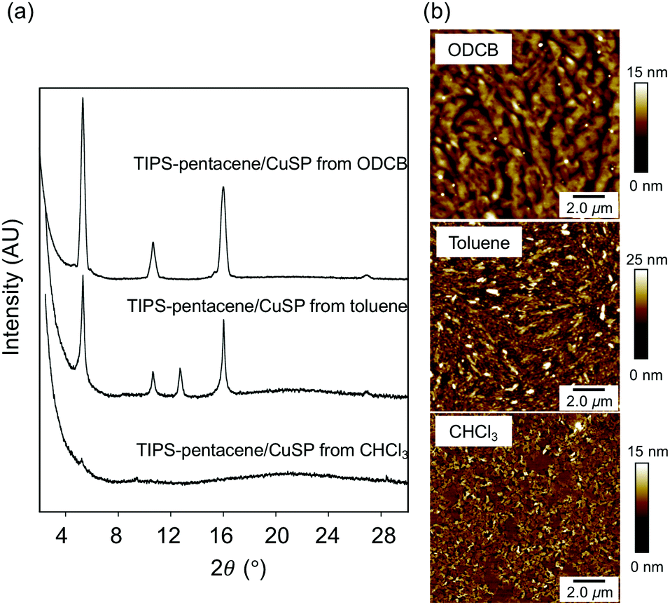 | ||
| Fig. 2 (a) XRD profiles of TIPS-pentacene/CuSP blend films spin-coated from various solvents. (b) AFM height images of the TIPS-pentacene/CuSP blend films. | ||
The blend films on quartz plates were also analyzed by polarized optical microscopy (POM). As shown in Fig. 3a, large spherulite textures were observed for the blend films spin-coated from ODCB. The blend film spin-coated from a toluene solution showed smaller spherulite textures; the film spin-coated from CHCl3 did not show large crystals. The different morphologies of the TIPS-pentacene in the blend films spin-coated from the various solvents were also examined by UV-vis absorption spectroscopy (Fig. 3b). The absorption spectrum of TIPS-pentacene in a CHCl3 solution showed three characteristic absorption bands in the 500–700 nm region; these bands originated from the first excited singlet state. A similar spectrum was observed for a film spin-coated from a CHCl3 solution of TIPS-pentacene/CuSP, indicating that, like the TIPS-pentacene in the solution state, the most of the TIPS-pentacene molecules in the polymer film existed in monomeric form. The fast evaporation of CHCl3 solution during the spin-coating process might disperse the TIPS-pentacene molecules in the polymer matrix before crystallization proceeded. An additional shoulder band at ∼700 nm was observed in the spectrum of the film obtained from toluene solution, which originated from the aggregated structure of TIPS-pentacene. The spectrum of the blend film spin-coated from ODCB solution showed broader absorption bands at approximately 600, 650, and 700 nm. These results reveal that most of the TIPS-pentacene molecules assembled to form crystals even in the presence of the polymer matrix. Notably, the absorbance from the CuPc core at ∼630 nm in the spectra of the blend films was overlapped by the strong absorption of the TIPS-pentacene because of the small amount of CuPc unit in the polymer matrix.
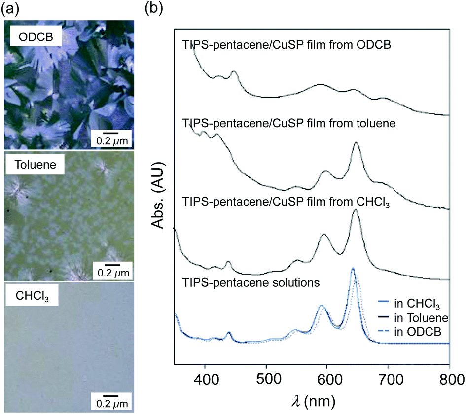 | ||
| Fig. 3 (a) POM images of the TIPS-pentacene/CuSP blend films. (b) Absorption spectra of TIPS-pentacene/CuSP blend films and TIPS-pentacene solutions. | ||
We used XPS to investigate the detailed structure in the blend films of TIPS-pentacene and CuSP spin-coated from ODCB and CHCl3 on the Si wafer substrates. The depth profiles of the film were collected by Ar+-ion sputtering with an etching rate of 2.7 nm min−1 for the film from ODCB and 3.2 nm min−1 for the film from a CHCl3 solution. All XPS peaks were referenced to the neutral C 1s peak at a binding energy of 284.8 eV. The peak intensities at binding energies corresponding to C 1s and Si 2p were plotted against the sputter time (Fig. 4). Notably, the Si 2p binding energies in the spectra of the TIPS-pentacene and SiO2 on the Si-wafer substrates were sufficiently different for each component to be identified (Fig. S3, ESI†). In addition, the peaks of N 1s or Cu 2p in the spectra of CuSP were difficult to observe because of the small atom%. The depth profiles of the blend film spin-coated from ODCB indicate that the TIPS-pentacene phase was located at the upper interface and mainly existed to a depth of ∼20 nm from the top interface in a blend film with a total thickness of ∼50 nm. This result is consistent with the aforementioned AFM analyses. On the other hand, the peak intensities of Si 2p corresponding to TIPS-pentacene in the CHCl3-processed blend film were relatively constant throughout the film thickness. This result indicated that the TIPS-pentacene molecules were distributed in the polymer film without clear phase segregation, which also agreed with the above results. We concluded that the TIPS-pentacene forms large crystals on the CuSP polymer layer via vertical phase segregation of the blend film deposited by a simple one-pot spin-coating process from ODCB solution.
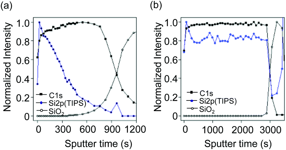 | ||
| Fig. 4 XPS depth profiles of a TIPS-P/CuSP blend films coated from (a) ODCB and (b) CHCl3 solutions on a Si substrate. | ||
OFET characteristics
Having successfully prepared vertically segregated organic semiconductor and polymer layers on the substrates via a one-pot solution process, we further fabricated OFET devices with a bottom-gate/top-contact configuration (Fig. 1a). Top-contact gold electrodes with a channel length (L) of 50 μm and a width (W) of 1000 μm were deposited onto blend films of TIPS-pentacene and star polymers of CuSP or PS4 spin-coated onto highly doped n-type Si(100) wafers with a 300 nm-thick surface layer of SiO2. The capacitance of the gate dielectric (Ctot) was estimated on the basis of the reported dielectric constants of CuSP or PS4. From the aforementioned results, the thickness of the polymer dielectrics was assumed to be 30 nm given that the total thickness of the blend film was 50 nm and the TIPS-pentacene crystals were 20 nm thick.The electrical transfer and output characteristics of the fabricated OFET devices are shown in Fig. S4 (ESI†). The reliability factors (r) for μeff of the OFET devices with CuSP and PS4 were also estimated (Fig. S4, ESI†, inset).37 When the gate bias was scanned between +10 and −50 V, the typical p-type accumulation mode was observed for the blend films spin-coated from ODCB. The devices with the blend films of TIPS-pentacene and CuSP or PS4 spin-coated from ODCB showed average μeff values of 0.10 ± 0.05 and 0.11 ± 0.09 cm2 V−1 s−1, respectively. Compared to the reported μeff values of 0.21 cm2 V−1 s−1 for vacuum-deposited pentacene-embedded OFET,34 these values are sufficiently high for solution-processed OFET devices. The on/off ratios of the drain current (Ion/Ioff) were greater than 106, which is beneficial for the memory device to clearly distinguish between the “0” and “1” digital states. As previously discussed, large crystal grains of TIPS-pentacene on the polymer dielectrics provided efficient charge transport pathways in the OFET devices. By contrast, the OFET device with the blend film spin-coated from toluene showed a low hole mobility of 1.0 × 10⁻³ cm2 V−1 s−1 at the maximum (Fig. S5a and b, ESI†). In addition, the OFET devices with embedded blend films coated from CHCl3 did not demonstrate transistor characteristics (Fig. S5c and d, ESI†). The lack of large TIPS-pentacene crystals or the polymer insulating layer on the surface disturbed the efficient charge transport in the OFET devices.
Memory characteristics
We confirmed that the blend film of TIPS-pentacene and CuSP prepared via a one-pot solution process showed vertical phase separation between the organic semiconductor and the polymer dielectrics and that this phase separation led to facile crystallization of the organic semiconductor, which is essential for high-performance OFET devices. The polymer dielectrics of CuSP function not only as a matrix but also as a memory material because the polymer has distinct charge-trapping sites, i.e., CuPc cores, that can trap hole charges upon application of a negative gate voltage. To investigate the memory properties of the CuSP-embedded OFETs, we operated the devices by alternately switching the gate bias (Vg) between −50 and +50 V as a pulse stimulus with a fixed drain voltage (Vd) of −50 V. As shown in Fig. 5a and Fig. S6 (ESI†), the transfer curve exhibited a negative shift after a negative gate voltage of Vg = −50 V was applied for 1 s (writing process). This result indicates that the hole charges accumulated in the TIPS-pentacene layer were injected and stored in the underlying CuSP layer, resulting in a built-in electric field opposite the applied Vg. The efficient injection of charge into the CuPc core in the polymer layer was achieved via the appropriate highest occupied molecular orbital (HOMO) energy levels of the CuSP and TIPS-pentacene of −5.2 and −5.1 eV, respectively (Fig. S7, ESI†). Conversely, upon application of a positive gate bias of +50 V to the OFET device, the transfer curve shifted in the positive direction, returning to its initial position. This operation is referred to as the erasing process, where the stored hole charges in CuSP are transferred back to the channel, implying that the device is categorized as a flash-type memory device. One may concern here the possibility of charge trapping in TIPS-pentacene molecules buried in the polymer layer. However, the OFET embedding a blend film of TIPS-pentacene and PS4 without CuPc core did not show any shift in the threshold voltage upon writing and erasing processes (Fig. 5b). This result confirms that the memory characteristics were derived from the CuPc core in the star polymer layer. The shift of Vth (ΔVth), which is referred to as the memory window, was evaluated to be 19.7 ± 5.5 V, which is similar to the reported memory window of ΔVth = 21 ± 1.03 V for a vacuum-deposited pentacene-based OFET memory device with embedded CuSP.33 The maximum memory ratio (i.e., the Ion/Ioff ratio at the reading gate voltage after the writing/erasing process) was ∼103 because of the intrinsic large Ion/Ioff value of the device (i.e., 106). The multiple switching durability of the OFET with CuSP was further evaluated through write-read-erase-read (WRER) cycle test. The drain current was read at Vg = −10 V with the fixed Vd = −50 V after repeating the writing and erasing operations with the continuous bias pluses of −50 V/50 V (Fig. 6a). After several cycles, the ION/IOFF ratio was maintained above 102 over 100 cycles (Fig. 6b).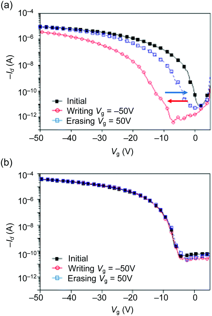 | ||
| Fig. 5 Transfer characteristics of OFET memory devices fabricated using (a) TIPS-P/CuSP blend films and (b) TIPS-P/PS4 blend films monitored at Vd = −50 V. | ||
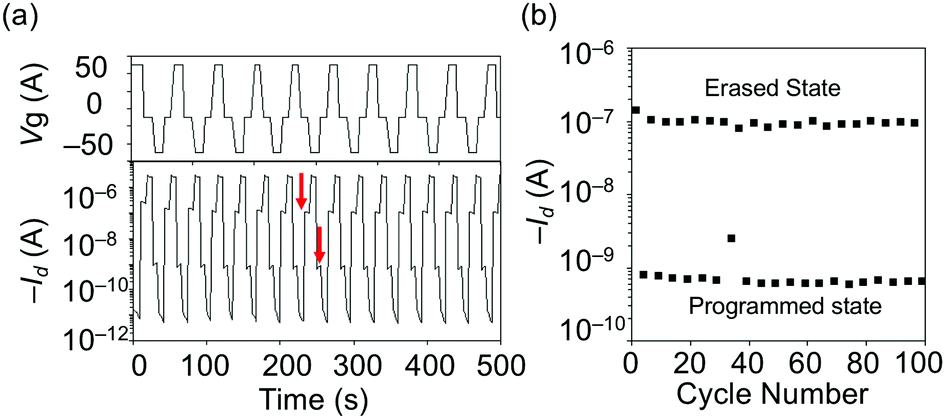 | ||
| Fig. 6 WRER test (a) and endurance characteristics (b) of the OFET memory device with TIPS-pentacene/CuSP blend films. | ||
Charge retention is also important when evaluating the nonvolatility of a memory device. To evaluate the memory retention characteristics, we monitored the drain current at Vg = −5 V after a writing operation at Vg = −50 V for 1 s and an erasing operation at Vg = +50 V for 1 s (Fig. 7). The difference in the drain on/off current was maintained at 102 for 12000 s. High stability of the stored charge was achieved because of the unique architecture of the star-shaped polymer, where the arm polymer chains surrounding the CuPc core assemblies restrain the leakage of the trapped charges.
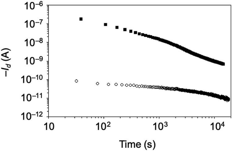 | ||
| Fig. 7 Retention time of the Id of the OFET memory device with TIPS-pentacene/CuSP blend films, as monitored at Vg = −5 V after writing (black squares) and erasing (white circles) operations. | ||
Conclusions
We have successfully developed high-performance solution-processed OFET memory devices using TIPS-pentacene and copper phthalocyanine-cored star-shaped polystyrene. The morphology and crystal structure of the TIPS-pentacene in the polymer blend film was found to be dependent on the solvent. We also found that the TIPS-pentacene/polymer film spin-coated from ODCB solution showed vertical phase separation, with large crystal grains of the organic semiconductor at the top surface, which is advantageous for OFET device applications. The OFET devices fabricated by the solution process using the blend films of TIPS-pentacene and CuSP exhibited a high charge carrier mobility with substantial memory characteristics. The novel methodology of using a polymer nano-floating gate to construct OFET memory in a one-pot solution process is a promising technique to prepare high-performance OFET memory devices and would be useful for fabricating flexible and large-area memory devices.Conflicts of interest
There are no conflicts to declare.Acknowledgements
We are grateful to Dr Hideyuki Yasufuku in Research Network and Facility Services Division (RNFS), NIMS for the XPS measurements and analyses. This work was partially supported by JSPS KAKENHI Grant (JP 21K05220, 18K14300), The Murata Science Foundation, and the Iketani Science and Technology Foundation. C.-F.H. acknowledges the support from the Ministry of Science and Technology, Taiwan (MOST108-2923-E-005-001-MY2).References
- T. Sekitani, T. Yokota, U. Zschieschang, H. Klauk, S. Bauer, K. Takeuchi, M. Takamiya, T. Sakurai and T. Someya, Science, 2009, 326, 1516–1519 CrossRef CAS PubMed.
- K. J. Baeg, D. Khim, J. Kim, B. D. Yang, M. Kang, S. W. Jung, I. K. You, D. Y. Kim and Y. Y. Noh, Adv. Funct. Mater., 2012, 22, 2915–2926 CrossRef CAS.
- S. J. Kim and J. S. Lee, Nano Lett., 2010, 10, 2884–2890 CrossRef CAS PubMed.
- W. L. Leong, N. Mathews, B. Tan, S. Vaidyanathan, F. Dotz and S. Mhaisalkar, J. Mater. Chem., 2011, 21, 5203–5214 RSC.
- M. Kang, K. J. Baeg, D. Khim, Y. Y. Noh and D. Y. Kim, Adv. Funct. Mater., 2013, 23, 3503–3512 CrossRef CAS.
- C. C. Shih, W. Y. Lee and W. C. Chen, Mater. Horiz., 2016, 3, 294–308 RSC.
- L. V. Tho, K. J. Baeg and Y. Y. Noh, Nano Convergence, 2016, 3, 10 CrossRef.
- J. S. Lee, Electron. Mater. Lett., 2011, 7, 175–183 CrossRef CAS.
- W. L. Leong, N. Mathews, B. Tan, S. Vaidyanathan, F. Dotz and S. Mhaisalkar, J. Mater. Chem., 2011, 21, 8971–8974 RSC.
- Y. H. Chou, Y. C. Chiu and W. C. Chen, Chem. Commun., 2014, 50, 3217–3219 RSC.
- C. Wu, W. Wang and J. F. Song, Appl. Phys. Lett., 2016, 109 CAS.
- W. Li, F. N. Guo, H. F. Ling, H. Liu, M. D. Yi, P. Zhang, W. J. Wang, L. H. Xie and W. Huang, Small, 2018, 14 Search PubMed.
- Y. Park, K. J. Baeg and C. Kim, ACS Appl. Mater. Interfaces, 2019, 11, 8327–8336 CrossRef CAS PubMed.
- F. Shiono, H. Abe, T. Nagase, T. Kobayashi and H. Naito, Org. Electron., 2019, 67, 109–115 CrossRef CAS.
- V. Coropceanu, J. Cornil, D. A. da Silva, Y. Olivier, R. Silbey and J. L. Bredas, Chem. Rev., 2007, 107, 926–952 CrossRef CAS.
- T. Ohe, M. Kuribayashi, R. Yasuda, A. Tsuboi, K. Nomoto, K. Satori, M. Itabashi and J. Kasahara, Appl. Phys. Lett., 2008, 93, 053303 CrossRef.
- J. Kang, N. Shin, D. Y. Jang, V. M. Prabhu and D. Y. Yoon, J. Am. Chem. Soc., 2008, 130, 12273 CrossRef CAS PubMed.
- R. Hamilton, J. Smith, S. Ogier, M. Heeney, J. E. Anthony, I. McCulloch, J. Veres, D. D. C. Bradley and T. D. Anthopoulos, Adv. Mater., 2009, 21, 1166–1171 CrossRef CAS.
- J. Smith, R. Hamilton, I. McCulloch, N. Stingelin-Stutzmann, M. Heeney, D. D. C. Bradley and T. D. Anthopoulos, J. Mater. Chem., 2010, 20, 2562–2574 RSC.
- L. H. Chou, Y. Na, C. H. Park, M. S. Park, I. Osaka, F. S. Kim and C. L. Liu, Polymer, 2020, 191 Search PubMed.
- L. Janasz, M. Borkowski, P. W. M. Bolm, T. Marszalek and W. Pisula, Adv. Funct. Mater., 2021, 2105456 Search PubMed.
- M. B. Madec, D. Crouch, G. R. Llorente, T. J. Whittle, M. Geoghegan and S. G. Yeates, J. Mater. Chem., 2008, 18, 3230–3236 RSC.
- D. K. Hwang, C. Fuentes-Hernandez, J. D. Berrigan, Y. N. Fang, J. Kim, W. J. Potscavage, H. Cheun, K. H. Sandhage and B. Kippelen, J. Mater. Chem., 2012, 22, 5531–5537 RSC.
- N. Shin, J. Kang, L. J. Richter, V. M. Prabhu, R. J. Kline, D. A. Fischer, D. M. DeLongchamp, M. F. Toney, S. K. Satija, D. J. Gundlach, B. Purushothaman, J. E. Anthony and D. Y. Yoon, Adv. Funct. Mater., 2013, 23, 366–376 CrossRef CAS.
- M. R. Niazi, R. P. Li, E. Q. Li, A. R. Kirmani, M. Abdelsamie, Q. X. Wang, W. Y. Pan, M. M. Payne, J. E. Anthony, D. M. Smilgies, S. T. Thoroddsen, E. P. Giannelis and A. Amassian, Nat. Commun., 2015, 6, 8598 CrossRef CAS PubMed.
- T. Makita, M. Sasaki, T. Annaka, M. Sasaki, H. Matsui, C. Mitsui, S. Kumagai, S. Watanabe, T. Hayakawa, T. Okamoto and J. Takeya, Appl. Phys. Lett., 2017, 110 Search PubMed.
- M. Lada, M. J. Starink, M. Carrasco, L. C. Chen, P. Miskiewicz, P. Brookes, M. Obarowska and D. C. Smith, J. Mater. Chem., 2011, 21, 11232–11238 RSC.
- W. H. Lee, D. Kwak, J. E. Anthony, H. S. Lee, H. H. Choi, D. H. Kim, S. G. Lee and K. Cho, Adv. Funct. Mater., 2012, 22, 267–281 CrossRef CAS.
- A. M. Gaikwad, Y. Khan, A. E. Ostfeld, S. Pandya, S. Abraham and A. C. Arias, Org. Electron., 2016, 30, 18–29 CrossRef CAS.
- J. H. Lee, Y. Seo, Y. D. Park, J. E. Anthony, D. H. Kwak, J. A. Lim, S. Ko, H. W. Jang, K. Cho and W. H. Lee, Sci. Rep., 2019, 9, 21 CrossRef PubMed.
- K. Kim, J. Hong, S. G. Hahm, Y. Rho, T. K. An, S. H. Kim and C. E. Park, ACS Appl. Mater. Interfaces, 2019, 11, 13481–13490 CrossRef CAS PubMed.
- Y. Diao, B. C. K. Tee, G. Giri, J. Xu, D. H. Kim, H. A. Becerril, R. M. Stoltenberg, T. H. Lee, G. Xue, S. C. B. Mannsfeld and Z. N. Bao, Nat. Mater., 2013, 12, 665–671 CrossRef CAS PubMed.
- J. Aimi, C. T. Lo, H. C. Wu, C. F. Huang, T. Nakanishi, M. Takeuchi and W. C. Chen, Adv. Electron. Mater., 2016, 2, 1500300 CrossRef.
- J. Aimi, P. H. Wang, C. C. Shih, C. F. Huang, T. Nakanishi, M. Takeuchi, H. Y. Hsueh and W. C. Chen, J. Mater. Chem. C, 2018, 6, 2724–2732 RSC.
- J. H. Chen, J. Anthony and D. C. Martin, J. Phys. Chem. B, 2006, 110, 16397–16403 CrossRef CAS PubMed.
- G. Giri, E. Verploegen, S. C. B. Mannsfeld, S. Atahan-Evrenk, D. H. Kim, S. Y. Lee, H. A. Becerril, A. Aspuru-Guzik, M. F. Toney and Z. A. Bao, Nature, 2011, 480, 504–508 CrossRef CAS PubMed.
- M. Sugiyama, S. Jancke, T. Uemura, M. Kondo, Y. Inoue, N. Namba, T. Araki, T. Fukushima and T. Sekitani, Org. Electron., 2021, 96, 106219 CrossRef CAS.
Footnote |
| † Electronic supplementary information (ESI) available. See DOI: 10.1039/d1ma01081f |
| This journal is © The Royal Society of Chemistry 2022 |