
 Open Access Article
 This Open Access Article is licensed under a
 Creative Commons Attribution 3.0 Unported Licence
Engineering Schottky-like and heterojunction materials for enhanced photocatalysis performance – a review
Priyanka
Kumari
*ab,
Nupur
Bahadur
*c,
Lingxue
Kong
 a,
Luke A.
O’Dell
a,
Andrea
Merenda
d and
Ludovic F.
Dumée
*efg
a,
Luke A.
O’Dell
a,
Andrea
Merenda
d and
Ludovic F.
Dumée
*efg
aDeakin University, Geelong, Institute for Frontier Materials, Waurn Ponds, 3216, Victoria, Australia. E-mail: pkumari@deakin.edu.au
bTERI-Deakin Nano-Biotechnology Centre (TDNBC), Teri Gram, Gwal Pahari, Gurugram 122003, Haryana, India
cTADOX® Technology Centre for Water Reuse, Water Resources Division, The Energy and Resources Institute (TERI), India Habitat Centre, Lodhi Road, New Delhi-110003, India. E-mail: nupur.bahadur@teri.res.in
dSchool of Science, RMIT University, 124 La Trobe Street, Melbourne, Victoria, Australia
eKhalifa University, Department of Chemical Engineering, Abu Dhabi, United Arab Emirates
fResearch and Innovation Center on CO2 and Hydrogen, Khalifa University, Abu Dhabi, United Arab Emirates
gCenter for Membrane and Advanced Water Technology, Khalifa University, Abu Dhabi, United Arab Emirates. E-mail: ludovic.dumee@ku.ac.ae
First published on 20th January 2022
Abstract
Photocatalysis with nanostructured semiconductors is one of the most widely used technologies for environmental remediation. However, the issues related to conventional photocatalysis such as fast recombination of photo-generated electron and hole pairs and poor redox abilities of the charge carriers need to be addressed to improve the properties and catalytic performance of semiconductor based photocatalysts. The engineering of metal/semiconductor interfaces to develop Schottky-like materials and semiconductor/semiconductor interfaces to design heterojunction materials offers spatial charge separation, leading to suppressed recombination of charge carriers and enhanced catalytic performance. Therefore, Schottky-like and heterojunction materials have emerged as a promising solution to the limitations associated with conventional photocatalysis. This review compares the fundamentals, various structures, configurations and charge transfer pathways of Schottky-like and heterojunction materials together. The physicochemical properties of recently developed Schottky-like and heterojunction materials were further correlated with the photocatalytic degradation of common dyes and persistent organic pollutants in wastewater. This review exemplifies the commonly used metals such as Ag, Au, Pt, Zn, and Bi and semiconducting materials such as TiO2, ZnO, CdS, g-C3N4, MnO2, Fe2O3, and BiVO4 for the preparation of Schottky-like and heterojunction materials. Furthermore, the challenges and the perspective towards the enhancement of materials design and properties of Schottky-like and heterojunction structures are also provided.
1 Introduction
Challenges associated with environmental pollution from chemicals may be remediated by using advanced oxidative processes and catalysis through selective and fast degradation of persistent organic pollutants (POPs).1 Efficient photo-catalyses however require (i) slow recombination of photo-generated electron and hole pairs and (ii) strong redox potential to support high electron transfer across the materials.2 The emergence of advanced nanostructured and nano-layered photo-catalysts has opened the path to multidisciplinary research towards the tailoring of physicochemical, structural and optoelectronic properties to promote enhanced catalysis of organic pollutants.The options for the enhancement of catalytic performance and visible light activation of the materials involve metal or non-metal doping of semiconductors3 and defect engineering in catalytic nanostructures such as graphene.4 The most promising engineering strategy involves the design of electronic barriers, which are introduced at the junction of a conductive and a semiconducting layer.5 The interface between the conductive layer, typically a metal or carbon surface, and the semiconducting material, often a metal oxide, may lead to the development of two types of junctions, either Ohmic or Schottky-like junctions.6 On the one hand, an Ohmic junction is formed when the semiconducting materials offer a higher work function than the conducting one.7 An Ohmic contact however offers a sustained flow of electrons between the metal and the semiconducting material in both forward and reverse biased directions, thereby hindering the separation of charge carriers and leading to poor photo-response capabilities.8 On the other hand, Schottky-like junctions are formed when semiconducting materials exhibit a lower work function than the conductive material, leading to a unilateral flow of electrons only in the forward biased direction, thus enabling efficient charge separation.6 Schottky-like materials have been particularly applied in photo-electronics, solar cells, H2 production and power rectifiers, and circuit applications, offering high current density, low forward voltage drop, and low power consumption, leading to high efficacy devices. The design of Schottky-like photocatalysts therefore supports efficient charge separation and enhanced transport of electrons and holes through the materials, subduing their recombination and foremost enhancing the catalysis.9
Another class of advanced photo-catalytic materials is referred to as heterojunctions, which are generated upon engineering of the intimate interfaces between at least two semiconducting materials offering different band-gaps.10,11 The major benefit of heterojunction fabrication over conventional doping is the efficient production of a larger density of charge carriers from the multiple semiconducting interfaces.11 Therefore, designing heterojunction structures may represent a scalable and cost-effective strategy to mitigate challenges associated with conventional photo-catalysts, since the interface between the two semiconducting materials may overcome the drawbacks associated with individual components.12 The nature of these multi-layered structures also offers opportunities to develop alternative catalytic processes, by combining photo, electro and thermal activation to further enhance the reactivity, kinetics and potentially selectivity of the catalysts.13 Multiple reviews are available, which elaborate the recent advances on Schottky junction solar cells.14–16 Reviews targeting the catalytic remediation of wastewater using Schottky-like materials are limited. Recently, a review covered the fundamentals, structures and photocatalytic applications of Schottky-like materials17 and to date, only one review has presented the correlation and paradox in the mechanism of Schottky barriers and surface plasmon effects for enhancing the photocatalytic reactions.18 Another review focused on the basic principles of heterojunction photocatalysts and their application towards various photocatalytic reactions.19 The most recently published review article on heterojunction based photocatalysts discussed the synthetic pathways, and different configurations of heterojunctions, and further correlated with photocatalytic applications such as H2 production, CO2 reduction and organic dye degradation.12
This review critically presents and compares Schottky-like and heterojunction materials to develop next generation photo-catalytic materials with an enhanced response rate and electron generation/transfer selectivity. The design and development of material configurations involving conducting/semiconducting layers in Schottky-like interfaces or as heterojunction-based structures is reviewed from a materials engineering and operation point of view. The physico-chemical properties and catalytic mechanisms of recently developed Schottky-like and heterojunction-based photocatalytic materials are discussed towards the degradation of common dyes and persistent organic pollutants to offer new perspectives on the integration of such materials into effective heterogeneous catalytic systems for wastewater degradation.
2 Structures and charge separation mechanisms of Schottky-like materials
The formation of Schottky-like barriers occurs at the junction of the metal and the n-type semiconducting materials when the work function (ϕM) of the metal is higher. The majority of charge carriers in p-type semiconductors are positive holes, which would attract electrons from the metal side, leading to the neutralization of the semiconducting material.20 Therefore, n-type semiconducting materials are generally used in the formation of Schottky-like barriers. The work function of a metal represents the energy required to accelerate an electron from the Fermi level of the metal to vacuum (Fig. 1(A)).18 Since metals are, by nature, more conductive than oxides, they exhibit a lower Fermi energy (EFermi) than semiconducting materials.18 The Fermi level of semiconducting materials lies just below their conduction band and the difference between the energies of the lowest occupied conduction band (CB) and vacuum energy is called, for semiconducting materials, the electro affinity (ηSM).21 As the semiconducting material and metal comes in contact during Schottky-like barrier generation, the electrons will flow from the higher EFermi of the semiconducting material to the lower EFermi of the metal, until an equilibrium stage is reached with a constant EFermi across both materials, called the band bending22 (Fig. 1(B)). The flow of electrons from the semiconducting material to the metal leads to a depletion of electrons within the semiconducting material, supporting the accumulation of positive holes within the semiconducting material but near the semiconductor/metal interface.22–24 Meanwhile, the electrons accumulate within the metal but near the very same interface to maintain electrical neutrality (Fig. 1(C)). This mechanism leads to the formation of a depletion layer at the junction, which generates a localised potential barrier for the charge carriers, referred to as the Schottky-like barrier (Fig. 1(C)). The charge carriers must overcome the Schottky-like barrier to continue migration across the metal/semiconductor interface.18 Schottky-like barriers work effectively for electron trapping, restricting the electron flow back to the semiconducting bulk material, which in turn reduces the recombination of photo-generated electron and hole pairs.25 Therefore, the Schottky like properties occurring at the metal/semiconductor interface further enhance the generation of reactive oxygen species (ROS), leading to an enhancement in the catalytic performance of the materials.26,27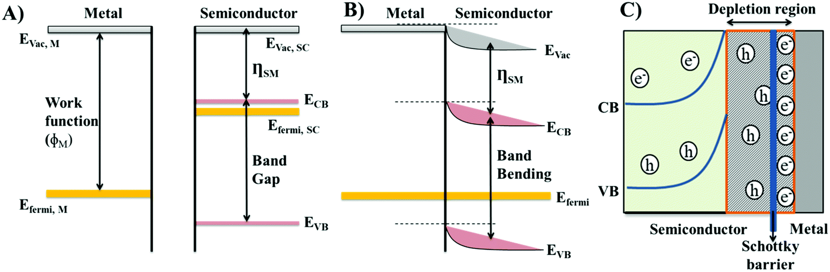 | ||
| Fig. 1 (A) Band structures of the metal and the n-type semiconducting material before contact. (B) Band structures of the metal and the n-type semiconducting material after contact. (C) Schematic representation of the flow of charge carriers and creation of a depletion region and Schottky-like barrier at the junction of the metal and the n-type semiconducting material. | ||
Surface plasmon resonance (SPR) is basically the oscillation of electrons at the junction between a semiconductor and metal.28 On the irradiation of light (electric field), the electron density on the metal gets redistributed leading to a decrease of electron density at one side of the metal, while on the other side of the metal the electron density increases.29 This creates an in-built electric field inside and outside the metal, which is in the opposite direction of the applied electric field, causing a series of charge density oscillations.30 The phenomenon of creation of an in-built electric field and oscillation of electrons are called as surface plasmon resonance (SPR) or localised surface plasmon resonance (LSPR).30 Upon irradiation with visible light, noble metal nanoparticles such as Ag, Au, and Pd also produce hot electrons due to the surface plasmon effect (SPR).31 These hot electrons possessing higher energies are able to cross the Schottky barrier and drift towards the CB of the adjacent semiconducting material, while the holes in the semiconducting materials start drifting towards the metal due to the intrinsic electromagnetic field.32 Therefore, the SPR effect is responsible for reversing the charge transfer mechanism at the metal/semiconductor interface.33 Under the SPR effect, the hot-electrons at the CB of semiconducting materials assist the photo-reduction of O2 to produce superoxide ions (˙O2−).34,35 The holes accumulated on the surface of metal nanoparticles assist the photo-oxidation of H2O molecules to generate hydroxyl radicals (OH˙).34
The fundamental influence of the Schottky barrier on the photocatalytic mechanism has been very well recognized.18 However, the SPR mechanism in photocatalytic enhancement still remains incoherent because the whereabouts of the excited hot electrons from metal to the photocatalyst are still underdeveloped and opposite to the basic law of Schottky barrier in which the electrons are supposed to migrate towards the metal surface from the photocatalysts (Fig. 2).36
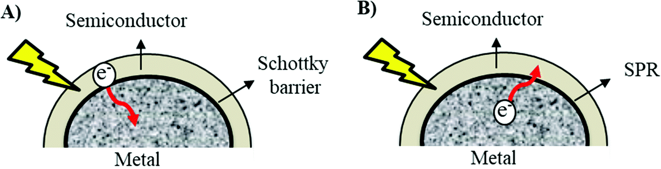 | ||
| Fig. 2 The proposed electron pathway during (A) Schottky barrier formation and (B) surface plasmon resonance (SPR). | ||
The structures of Schottky-like materials fall into four main categories – conventional, core–shell, 2D nano-sheet, and multi-junction structures8 (Fig. 3). The conventional Schottky-like structures are formed when the grouping of metal and semiconducting materials is not precisely controlled, leading to scattered deposition of metal nanoparticles across the surface of the semiconducting materials, as shown in the schematic representation in Fig. 3(A).8,37 Conventional Schottky-like structures such as Pt/TiO2 were fabricated by immersing and photo-radiating TiO2 nano-sheets under UV light in a H2PtCl6 solution, leading to the reduction of the platinum ions in solution to Pt metal on the surface of TiO2 nano-sheets.38 H2PtCl6 was also added to a TiO2 nanotube suspension, followed by stirring and solvent evaporation, leading to the formation of powdered nano-composite materials with 2 nm sized metal nanoparticles randomly scattered at the surface of a semiconducting core. Calcination of the powdered nano-composite in a reducing atmosphere led to the design of conventional Pt/TiO2 nanotubes with Schottky-like properties.39 Chemical vapour deposition was also used to synthesize conventional Schottky-like structures by vaporizing HAuCl4 at high temperature and subsequently blowing the vapours onto the surface of TiO2 nanorods at a lower temperature under an inert gas atmosphere, leading to the fabrication of Au/TiO2 nanorods.40 Metal Au nanoparticles of size 20 nm were deposited uniformly on the surface of TiO2 nanorods, shown in the TEM image of Au/TiO2 exhibiting a conventional Schottky-like structure in Fig. 3(A).40 The morphology and specific surface area (SSA) of the semiconducting materials in the conventional Schottky-like structure did not change significantly due to nano-sized deposition of metal particles (2–20 nm). The intrinsic properties of spherical metal nanoparticles do not allow intimate contact with the semiconducting materials, which leads to insufficient separation of charge carriers. Therefore, new structures of Schottky-like materials need to be explored.
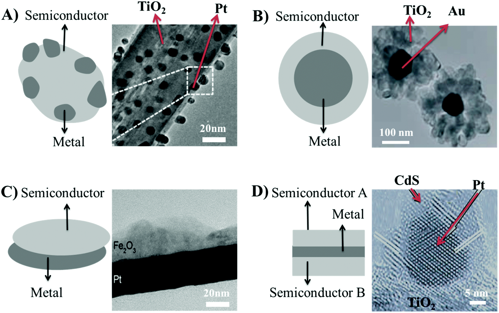 | ||
| Fig. 3 (A) Schematic representation of the conventional Schottky-like structure and TEM image of the Au/TiO2 junction exhibiting the conventional Schottky-like structure, reprinted with permission from Wiley;40 (B) schematic representation of the core–shell structure and TEM image of flower like Au/TiO2 nanostructures exhibiting the core–shell Schottky-like structure, reprinted with permission from Wiley;44 (C) schematic representation of the 2D nanosheet Schottky-like structure and TEM image of Pt/Fe2O3 exhibiting the formation of nanosheet Schottky-like structure reprinted with permission from Elsevier;50 (D) schematic representation of multi-junction Schottky-like structure and TEM image of the CdS/Au/TiO2 multi-junction Schottky-like structure, reprinted with permission from Springer.53 | ||
Core–shell structures are formed by encapsulating metal nanoparticles within semiconducting materials, resulting in a strong contact between the metal and the semiconducting material at the interface,41 as shown in the schematic in Fig. 3(B). The core–shell structures also enable efficient charge separation, thus preventing agglomeration and providing protection to the metal surface against coalescence and corrosion during heat treatment processes or, if exothermic, photocatalytic reactions.42,43 The synthesis of core–shell Schottky-like structures such as Au/TiO2 involved processes such as the hydrothermal preparation of core Au metal nanoparticles from the mixture of HAuCl4 and Na3C6H5O3 in sodium citrate solution under vigorous stirring. The solution containing core Au metal nanoparticles was transferred to an autoclave, followed by the addition of TiF4 solution and continuous heating for 48 h, which led to the aggregation of TiO2 crystallites on the surface of Au nanoparticles. The process led to the synthesis of core Au metal nanoparticles of size 50–150 nm, followed by aggregation of TiO2 crystallites in a shell-like pattern on the surface of Au nanoparticles as shown in the TEM image in Fig. 3(B).44 The core shell structures allowed the manipulation of the crystallite size of the metal core depending on the application, simply by injecting the metal precursor sol into the voids.44,45 The core shell Schottky-like structures also induced selectivity towards target pollutants as only the chemical species permeable through the outer inorganic shells could access the interior metal core and undergo metal catalysed reactions.46 The core shell structures offer several advantages over conventional Schottky structures; therefore, it is one of the sought after synthetic approaches to achieve higher selectivity and catalysis of pollutants.44,47
Two-dimensional (2D) nano-sheets of semiconducting metal oxides can offer superior photo-electrochemical properties due to their chemically active facets and edges, as well as a higher specific surface area (SSA), compared to bulk particles, thereby providing a higher density of photo-electro active sites.48 TiO2 nano-sheets exhibited a SSA of up to 250 m2 g−1, while commercial P-25 anatase TiO2 nanoparticles only exhibited a SSA of up to 50 m2 g−1.49 The deposition of metal oxide 2D nano-sheets onto metal substrates to develop Schottky-like structures is therefore highly sought after (Fig. 3(C)). The fabrication of 2D Fe2O3 nano-sheets on Pt metal substrates was achieved using area-selective atomic layer deposition, which led to the formation of clearly defined interfaces between the Fe2O3 layer and the underneath Pt substrate, as shown across the TEM image in Fig. 3(C).50 Such an arrangement provides Schottky-like characteristics to the material. Atomic layer deposition offered precise control over the thickness of the metal oxides at the atomic level alowing for the synthesis of metal oxide coatings with a 2D structured morphologies, which provided Schottky-like characteristics to the materials.51
Multi-junction Schottky-like structures can also be formed by sandwiching metal nanoparticles between two semiconducting materials, as schematically represented in Fig. 3(D).52 The multi-junction Schottky-like structures endow more efficient charge separation than any other structures as the sandwiched metal nanoparticles act as an electron mediator. This configuration supports fast carry-over of electrons from the conduction band (CB) of one semiconductor A, with a higher oxidation potential, to the valence band (VB) of the semiconductor B, with a higher reduction potential.52 Therefore, spatial separation of charge carriers leads to the occurrence of oxidation reactions on semiconductor A, while semiconductor B only allows reduction reactions to happen.52 An example of a multi-junction CdS/Au/TiO2 was fabricated by a two-step reaction, whereby the first step involved the addition of TiO2 particles in HAuCl4 and NaOH solution, followed by stirring and solvent evaporation. The second step involved the UV-assisted reaction between sulphur and cadmium perchlorate to support the deposition of CdS onto the surface of Au/TiO2, thus providing multi-junction Schottky-like characteristics to the composite material.53 The structure between CdS/Au/TiO2 is shown in the TEM image in Fig. 3(D), illustrating TiO2 nanosheets anchored with Au nanoparticles of size 3.5 nm deposited by a solvothermal method, and further decorated with a 1.5 nm thin coating of CdS by UV-assisted deposition.53 The sandwiched Au nanoparticles act as the electron-transfer system, enabling efficient separation of charge carriers between TiO2 and CdS. Therefore, three component multi-junction systems are expected to show superior properties and performances to single or two component systems.
2.1 Physicochemical properties and catalytic performance of Schottky-like materials
The physicochemical properties such as morphology, and the structural, optical, and electrochemical properties of different Schottky-like materials are discussed and correlated to their catalytic performance, to understand the relationship between the properties of the materials and their enhanced catalytic behaviours.2.1.1.1 Ag/ZnO conventional structures. ZnO nanorods were fabricated by the sol–gel method followed by photo-reduction of AgNO3 solution to Ag nanoparticles on the tip of ZnO nanorods, leading to the formation of Ag decorated ZnO exhibiting Schottky-like properties (Table 1, entry 1).54 The adhesion between the Ag nanoparticles produced from the photo-reduction method and the photo-catalyst was weak as the reaction was not precisely controlled at the atomic level. The Ag incorporated ZnO nanorods showed intense optical absorption in the visible range from 400–700 nm due to the SPR effect of the Ag nanoparticles.54,55 Therefore, under visible light irradiation, the electrons generated on the surface of Ag due to the SPR effect migrated to the CB of ZnO and produced reactive oxygen species to mediate photo-catalytic activities. Meanwhile, under UV light irradiation, the Ag/ZnO interface enabled the migration of photo-generated electrons from ZnO to the Ag nanoparticles, acting as an electron sink, thus leading to enhanced charge separation and photo-catalytic performance compared to bare ZnO nanorods.54 The kinetic constant of the photo-catalytic degradation of MB dye using Ag/ZnO nanorods was 7.6 × 10⁻³ min−1, while bare ZnO nanorods showed a degradation kinetic constant of 5.5 × 10⁻³ min−1.
| Entry | Schottky-like structure | Type | Fabrication technique | Specific surface area (SSA) (m2 g−1) | Band-gap (eV) | Photocurrent density (mA cm−2) | Target pollutant (mg L−1) | Kinetic constant (k) (10−3 min−1) | Ref. |
|---|---|---|---|---|---|---|---|---|---|
| 1 | Ag/ZnO | Conventional | Sol–gel and photo-reduction | — | 3.37 | — | Methylene blue, (2) | 7.6 | 54 |
| 2 | Ag/TiO2 | Conventional | Solvothermal photo-reduction | 135 | 2.78 | — | Rhodamine B, (10) | 16.1 | 56 |
| 3 | Au/TiO2 | Conventional | Sol–gel | — | 3.20 | — | Methylene blue, (10) | 16.1 | 59 |
| 4 | Au/CdS | Core–shell | Solvothermal | — | — | 7 × 10⁻³ | Rhodamine B, (0.35) | 26 | 62 |
| 5 | Zn/SiO2 | Core–shell | Sol–gel | 36 | 3.0 | — | Methyl violet, (3.5) | 9.5 | 65 |
| 6 | Zn–Fe2O4/ZnO | Core–shell | Sol–gel | 1.8 | — | Methylene blue, (10) | 8.5 | 66 | |
| 7 | Bi/g-C3N4 | Nanosheets | Polymerization and hydrothermal | 57 | — | — | Nitric oxide, (0.6) | 120 | 67 |
| 8 | Bi/ZnwO4 | Nanosheets | Solvothermal | 30 | — | 1.25 × 10⁻³ | Nitric oxide, (0.4) | 67 | 68 |
| 9 | CdS/Ag/TiO2 | Multi-junction | Hydrothermal | 386 | 1.57 | 6 | Nitrobenzene, (30) | 20 | 69 |
| 10 | CdS/Au/ZnO | Multi-junction | Hydrothermal and pulse laser | — | — | 4.5 | Methylene blue, (0.3) | 13.3 | 70 |
2.1.1.2 M/TiO2 conventional structures (M = Ag, Au). A conventional Schottky-like Ag/TiO2 structure was fabricated by synthesising TiO2 microspheres by a solvothermal method and further decorating them with Ag nanoparticles by photo-reduction (Table 1, entry 2).56 The TiO2 microspheres showed a slight decrease in SSA from 159 to 135 m2 g−1 upon incorporation of Ag nanoparticles, which tend to occupy the pores of the catalyst in a random distribution in conventional Schottky-like structures.56 However, many studies also revealed an increase in the surface area when semiconducting materials are modified with metal nanoparticles. For instance, Ag decorated ZnO photocatalysts synthesised by a hydrothermal method showed a SSA of 18 m2 g−1, higher than the SSA of bare ZnO (14 m2 g−1).57 Another demonstration of Ag loaded ZnO micro-flowers prepared by hydrothermal method showed a SSA of 5.8 m2 g−1, exhibiting no evident change compared to bare ZnO with a SSA of 5.7 m2 g−1.58 The variation in the trend of surface area may be dependent on different methods of synthesis and processes.34 The band-gap of the Ag/TiO2 underwent a red shift and was reduced to 2.2 eV due to typical band alignment causing band bending in Schottky-like structures (Table 1, entry 2).56 Ag/TiO2 supported the photo-catalytic degradation of Rhodamine B, leading to a kinetic constant of 16 × 10−3 min−1, while bare TiO2 microspheres exhibited a lower catalytic efficiency with a kinetic constant of 5 × 10⁻³ min−1.56
Conventional Schottky-like Au/TiO2 structures were synthesized by the sol–gel method (Table 1, entry 3)59 and the impact of the variation of the Au nanoparticles size distribution over the catalytic properties of the materials was investigated. The Au/TiO2 structures with Au nanoparticles of size 15 nm exhibited maximum photocatalytic efficiency for the degradation of methylene blue (MB) with a kinetic constant of 16.1 × 10⁻³ min−1. Smaller (5 nm) Au nanoparticles anchored on TiO2 nanospheres, exhibited a lower photocatalytic performance with a kinetic constant of 10.5 × 10⁻³ min−1. The smallest metal nanoparticles (<5 nm) showed transitioning from metallic to molecular electronic states due to the quantum confinement effect, which in turn affected the charge transfer and separation abilities, thus lowering the catalytic activity.60 Nevertheless, the Au/TiO2 structures with larger sized Au nanoparticles (30 nm) exhibited a lower photocatalytic efficiency for the degradation of MB with a kinetic constant of 4 × 10⁻³ min−1 due to the poor contact with the surface of TiO2, leading to a lower catalytic performance.59,61 Therefore, the performance of the Schottky-like structures appeared to be highly dependent on the shape and size of metal nanoparticles and the contact at the metal and semiconductor interface.59,60
2.1.2.1 Au/CdS. A core–shell Schottky-like structure comprising Au metal nanoparticles as the core and CdS nanocrystals surrounding the Au metal, was synthesised by a wet-chemical and precisely controlled hydrothermal route (Table 1, entry 4).62 The CB of CdS is at −1 eV and the Fermi energy of Au nanoparticles is set at a less negative potential of +0.5 eV. Therefore, the Au metal acts as a good electron scavenger, leading to the storage of electrons on the Au metal and the formation of a Schottky-like barrier at the junction.62 The core–shell Au/CdS exhibited an almost two times higher transient photocurrent density of 7 μA cm−2 than pristine CdS and degraded the rhodamine B solution with a kinetic constant of 26 × 10−3 min−1 (Table 1, entry 4).62 As the thickness of the CdS shell increased from 9 to 18 nm, the kinetic constant of photocatalytic degradation also increased from 26 to 60 × 10−3 min−1 due to an increase of the charge carriers and electron transfer rate within the thicker shell. Another study exhibiting an increase of the CdS outer shell thickness by electrochemical deposition on Au inner metal core showed a sudden rise and fall of photocatalytic performance. When the CdS thickness increased from 1 to 7 nm, a spike in the photocurrent density to 75 μA cm−2 was observed. Further increase of CdS thickness to 12 nm led to up to 2 times decrease of the photocurrent density.63 The increased shell thickness may attenuate the light absorption capacity of the semiconducting materials, which further deteriorates the production of hot electrons.64 Moreover, the increased shell thickness also leads to an increase in the distance between the photo-generated hot electrons on the surface of the outer shell and the inner metal core, resulting in more recombination of electron and hole pairs, hence reduced photocurrent density and photocatalytic performance.64
2.1.2.2 Zn/MxOx (MxOx = SiO2, Fe2O3). Another core–shell structure involving Zn metal encapsulated by the SiO2 shell was fabricated by the sol–gel method (Table 1, entry 5).65 The band-gap of pristine SiO2 materials is generally very high, about 5.2 eV, and unsuitable for light harvesting activities. However, the core–shell Zn/SiO2 structures showed significant red-shifting of the band-gap to 3.0 eV due to band bending of the CB of SiO2 to the Fermi level of Zn metal, enabling the composite material to absorb light at a lower energy, suitable for photocatalytic applications.65 Zn/SiO2 also exhibited a higher SSA (32 m2 g−1), compared to bare SiO2 (12 m2 g−1), which facilitates the core shell structure towards adsorption and mass transfer of reactant molecules such as reactive oxygen species.65 Therefore, the photocatalytic degradation of methyl violet dye using Zn/SiO2 showed a kinetic constant of 11.6 × 10⁻³ min−1, about two times higher than that of pristine SiO2 (5.1 × 10⁻³ min−1).65
A magnetic core–shell Schottky-like material was fabricated by incorporating a magnetite core of Zn–Fe2O4 synthesised by hydrothermal method, followed by the immobilization of a ZnO shell on the surface (Table 1, entry 6).66 The Zn–Fe2O4/ZnO catalyst can be magnetically separated after every use due to the presence of the magnetite core, which enhanced the reusability of the catalyst. The magnetite core also enabled visible light activation of the composite catalyst as the band-gap of the core shell Zn–Fe2O4/ZnO was reduced to 1.8 eV, compared to the band-gap of ZnO (3.2 eV).66 Therefore, Zn–Fe2O4/ZnO led to the photocatalytic degradation of MB dye with a kinetic constant of 8.5 × 10⁻³ min−1 under the irradiation of visible light.66
2.1.3.1 Bi/MxOx (MxOx = g-C3N4, ZnwO4). 2D Bi/g-C3N4 nanosheet Schottky-like structures were fabricated by synthesizing g-C3N4 nanosheets under high temperature conditions by polymerization of urea and further decorating them with Bi nanospheres in an autoclave by the hydrothermal method (Table 1, entry 7).67 The TEM micrographs of Bi/g-C3N4 nanosheets suggest a close contact between the metal and the semiconducting material, leading to the favourable transfer mechanism of photo-generated charge carriers at the interface.67 The CB of g-C3N4 is at a negative potential of −1.12 eV, while the Fermi energy of Bi became less negative at −0.17 eV. This trend allowed the flow of electrons from the CB of g-C3N4 to the Fermi level of Bi metal, making this structure a good electron sink to carry efficient charge separation.67 Pristine g-C3N4 nanosheets led to the degradation of NO with a kinetic constant of 75 × 10−3 min−1. 2D Bi/g-C3N4 nanosheets exhibited high photocatalytic efficiency towards the removal of NO with a kinetic constant of 120 × 10−3 min−1, showing an enhancement in the catalytic performance by a factor of 1.7.67
The anchoring of Bi metal onto the surface of ZnWO4 microspheres, synthesised by the solvo-thermal method, was also demonstrated (Table 1, entry 8).68 The formation of Schottky-like structures between Bi and ZnWO4 enhanced the transient photocurrent density from 0.3 to 1.2 μA cm−2 and led to photocatalytic degradation of NO with a higher kinetic constant of 67 × 10−3 min−1 than those of bare ZnWO4 (6 × 10⁻³ min−1) and Bi (27 × 10−3 min−1).68 The abundant availability and low cost of Bi metal also makes it a good substitute for noble metals such as Ag and Au to develop Schottky-like junctions with semiconducting materials.67
2.1.4.1 CdS/M/MxOx (M = Ag, Au and MxOx = TiO2, ZnO). The coupling of semiconductor/metal/semiconductor leads to the development of multi-junction Schottky-like structures. The formation of multi-junction Schottky-like structures by decorating TiO2 nanorods with Ag nanoparticles, followed by the deposition of a CdS coating via hydrothermal synthesis was demonstrated (Table 1, entry 9).69 The entrapment of Ag nanoparticles between the TiO2 and CdS coatings was confirmed from TEM micrographs.69 The photo-generated electrons start to migrate from the CB of CdS (−0.7 eV) located at a more negative potential vs. NHE (normal hydrogen electrode), than the CB of TiO2 (−0.3 eV) via the sandwiched Ag nanoparticles to TiO2 nanorods and undergo recombination reactions with the holes present at the VB of TiO2. The flux of electrons creates a Schottky-like barrier at the interfaces, leading to the concentration of holes on the surface of the CdS, and electrons on TiO2 nanorods. Therefore, the relay of electrons in the multi-junction structures from the CdS layer to Ag metal and then to the TiO2 nanorods leads to efficient charge separation and hence an enhanced transient photocurrent density of 4.3 mA cm−2. The multi-junction TiO2/Ag/CdS also exhibited band bending with an effective band-gap of 1.56 eV, much lower than those of pristine TiO2 (3.2 eV) and CdS (2.5 eV), enabling visible light activation of the composite material. Therefore, the photocatalytic degradation of nitrobenzene under visible light by the TiO2/Ag/CdS multi-junction structure showed a kinetic constant of 16 × 10−3 min−1, which is at least two times higher than that for pristine TiO2 and CdS.69
The fabrication of multi-junction structures between CdS/Au/ZnO (Table 1, entry 10), in which ZnO nanorods were deposited on the ITO (Indium Tin Oxide) substrate by a hydrothermal method followed by the deposition of Au and CdS on the surface of ZnO by pulse laser ablation, was also demonstrated. The ablation of the Au target by pulse laser deposited about 10 nm sized Au nanoparticles and the CdS target deposited a 25 nm thick coating of CdS on the Au decorated ZnO nanorods. The multi-junction structures of CdS/Au/ZnO improved the electron flux and separation of photo-generated charge carriers in a similar mechanism described above, leading to a high transient photocurrent density of 4.5 mA cm−2, compared to the single junction structures between CdS/ZnO (1.5 mA cm−2) and Au/ZnO (0.05 mA cm−2). The kinetic constant for the photocatalytic degradation of the MB dye using multi-junction Schottky-like CdS/Au/ZnO nanorods was 13.3 × 10⁻³ min−1, higher than those of CdS/ZnO (10.3 × 10⁻³ min−1) and Au/ZnO (9.2 × 10⁻³ min−1).
2.2 Concluding remarks and strategies for improving Schottky-like materials
To conclude, several fabrication routes and photo-catalytic applications of Schottky-like nanostructures of various shapes, sizes and compositions have been investigated. Conventional Schottky-like materials exhibited a lower catalytic efficiency for the degradation of pollutant molecules such as methylene blue and rhodamine B dyes with kinetic constants in the range of 7.6–16 × 10−3 min−1 due to poor contact at the interface and uncontrolled synthesis causing agglomeration of metal nanoparticles on the surface of semiconducting materials. The core–shell structures provide close contact at the metal/semiconductor junctions, leading to an efficient charge transfer across the materials and hence enhancing the catalytic degradation of dyes such as methylene blue with kinetic constants in the range of 8.5–26 × 10−3 min−1. 2D nanosheets offer superior chemically active facets and edges, and enhanced surface area, leading to enhanced photo-electrochemical properties due to which the catalytic efficiency of the materials for the degradation of gaseous pollutants responsible of ozone depletion such as nitric oxide gas is higher than that of any other Schottky-like nanostructures with kinetic constants in the range of 60 – 120 × 10−3 min−1. The multi-junction Schottky-like materials allow greater charge separation than any other structures as the sandwiched metal nanoparticles act as an electron mediator, leading to a suppressed recombination rate and enhanced catalysis of pollutants such as methylene blue with kinetic constants in the range of 13–20 × 10−3 min−1. Challenges related to the synthesis of materials used for conventional Schottky-like structures remain primarily related to the agglomeration of metal nanoparticles in solution, leading to reduced catalytic efficiency. The development of core–shell and multi-junction Schottky structures was found to limit or prohibit agglomeration and therefore improve processability. The encapsulation or sandwiching of metal nanoparticles at the nanoscale with appropriate semiconducting materials is a particularly promising approach that benefits from the enhanced charge transfers at the interfaces, but yet requires complex synthesis procedures. The fabrication of Schottky-like materials, however, mostly employs the use of noble metals such as Au, Ag, and Pt to couple with semiconducting materials, which are present in scare quantity in nature and are also very costly. The use of conductive non-noble metals or alloys such as stainless steel needs to be explored towards the next generation of more scalable Schottky-like materials.3 Types, configuration and charge separation mechanism of heterojunctions
The charge carrier dynamics of the semiconductor/semiconductor heterojunction involves the creation of a space-charge region at the interface of the semiconducting materials from the migration of charge carriers.71 The diffusion of electron and hole pairs across the space charge region generates an internal electric field, which in turn directs the electrons and holes to travel in the opposite direction.72 This leads to the separation of charge carriers as electrons get transferred to the CB of the semiconductor with a higher reduction potential, while the holes get transferred to the VB of the semiconductor with a high oxidation potential.10,72 Therefore, the charge carrier dynamics of the heterojunction materials leads to more effective charge separation, rapid charge transfer mechanism, and improved lifetime of the electron and hole pairs, leading to enhancement of the photocatalytic efficiency.Conventional heterojunction structures are classified into four main categories, including type-I, type-II, type-III, and direct Z-scheme, defined based on the respective alignment of the conduction band (CB) and the valence band (VB).19,73 In a type-I heterojunction, the CB and VB of the semiconductor material A will be higher and lower, respectively, than the bands of semiconductor B; therefore, the accumulation of electrons and holes will only occur at the CB and VB, respectively, of the semiconductor B, as shown in Fig. 4(A).1 The accumulation of both electrons and holes occurs on the same semiconductor material in type-I heterojunction; therefore, such separation of charges is not highly effective as charge carriers can still undergo fast recombination.1
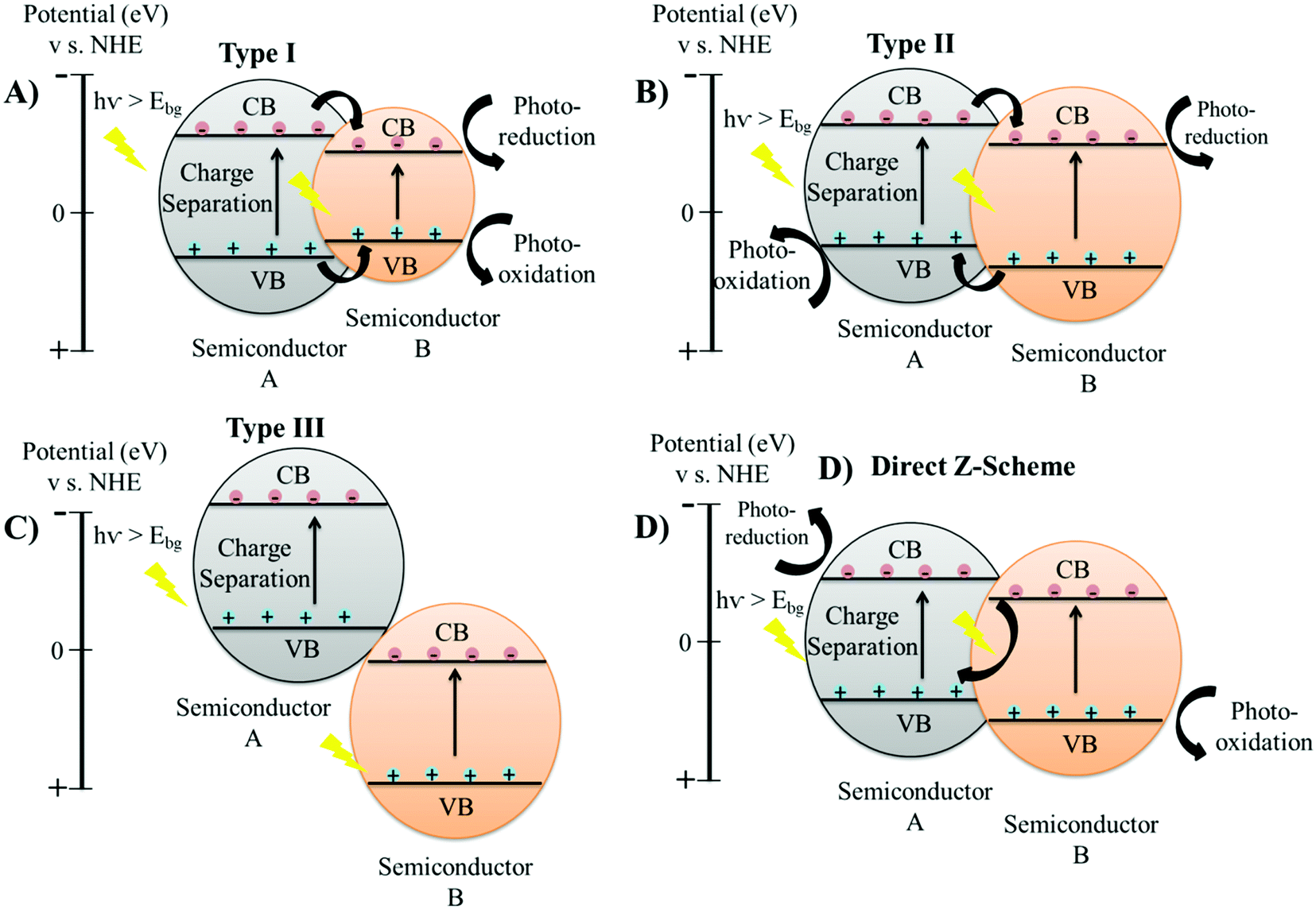 | ||
| Fig. 4 Spatial arrangements of different heterojunction structures: (A) type I; (B) type II; (C) type III and (D) direct Z scheme. | ||
In type-II heterojunctions, both CB and VB of semiconductor A will be higher than those of semiconductor B (Fig. 4(B)).74 Type-II heterojunctions therefore allow for the accumulation of electrons across the CB of semiconductor B, while holes will accumulate at the VB of semiconductor A, hence leading to very efficient charge separation.74 Although type-III heterojunctions are similar to type-II, both CB and VB in semiconductor A will be higher compared to semiconductor B, putting the bands very far apart and thereby preventing direct overlap, which is not suitable for mediating the spatial separation of electron and hole pairs (Fig. 4(C)).75 Type-II heterojunctions have been deemed the most suitable metastable structures for semi-conducting applications, and have been explored for a range of catalytic reaction control.19 However, type II heterojunctions also possess a major inadequacy from the thermodynamic perspective as improved charge separation efficiency does not compensate the reduced redox ability of the semiconducting materials, desirable for photocatalytic applications.76 The type II heterojunction materials allow the accumulation of photo-generated electrons and holes on semiconducting materials with weak reduction potential and weak oxidation potential, respectively.77 This kind of charge separation impairs the involvement of charge carriers in catalytic reactions. The electrostatic attraction between opposite charge-carriers in a semiconducting material, concurrently inhibits the flow of electrons from one semiconductor to the other semiconductor in type II heterojunction structures.78 Therefore, the theoretical charge transfer mechanism of a atype II heterojunction is difficult to realize because the electrostatic repulsive forces are great enough to suspend the flux of photo-generated charge carriers. Besides this, the charge transfer mechanism also leads to the reduction of the overall redox ability of type II heterojunctions.
The direct Z-scheme heterojunction shows a similar band alignment to that of type-II heterojunctions, but the direction of charge is opposite (Fig. 4(D)).79 Direct Z-scheme heterojunctions are also termed as S-scheme heterojunctions.80 A direct Z-scheme heterojunction consists of staggered band alignment, with charge transfer mechanism completely different from that of a type II heterojunction.79,81 The photo-generated electrons in the conduction band of the semiconducting material with a high reduction potential (semiconductor B) and holes in the valence band of the semiconducting material with a high oxidation potential (semiconductor A) are reserved for photocatalytic reactions.79 When two semiconductors come in close contact, initially the diffusion of electrons occur from semiconductor B possessing a high reduction potential to semiconductor A with a high oxidation potential.82 This creates a depletion region at the interface on the side of semiconductor B and an accumulation region on the side of semiconductor A, due to which the semiconductors A and B become negatively and positively charged, respectively. This internally generated electric field leads to the acceleration of photo-generated electrons from the CB of semiconductor A to the VB of semiconductor B, opposite to the charge transfer mechanism of type II heterojunctions. Moreover, close contact of the two semiconductors aligns the Fermi energy of each semiconductor to the same level leading to band bending.82 Band bending further supports the flux of electrons from the CB of semiconductor A to the VB of semiconductor B.83 Therefore, physical factors such as an internal electric field, band bending and coulombic forces drive the recombination of less powerful electrons from the CB of semiconductor A with a lower reduction potential to the inadequate holes present in the VB of semiconductor B with a lower oxidation potential.84 Thus, the redox affinity of the direct Z-scheme/S-scheme is maintained as the charge transfer mechanism eliminates useless charge carriers and preserves the powerful photo-generated electrons and holes separately on semiconductor B and A, respectively.85 Therefore, the Z-scheme heterojunctions not only improve the separation of charge carriers by allowing partial recombination reactions but also retain the strong redox abilities of the separated electron and hole pairs.86
3.1 Physicochemical properties and catalytic performance of heterojunctions
The physicochemical properties of heterojunction materials are dependent on the materials and synthesis routes employed, which in turn dictate the overall catalytic efficiency of the heterojunctions.87 The correlation of material dependent physicochemical properties with catalytic performance of the heterojunctions is discussed in the following section.3.1.1.1 FeS2/g-C3N4. A type I heterojunction between FeS2 and g-C3N4 was realised by calcination, liquid exfoliation and in situ deposition of FeS2 on g-C3N4via the hot injection route (Table 2, entry 1).88 The CB and VB of g-C3N4 were −1.28 and +1.62 eV, respectively vs. NHE. Similarly, FeS2 showed CB and VB at −0.5 and +0.8 eV, respectively. Therefore, the photo-generated electrons were transferred from the CB of g-C3N4 to the CB of FeS2 and holes from the VB of g-C3N4 to the VB of FeS2, exhibiting a typical type I charge transfer mechanism. The TEM micrograph of FeS2/g-C3N4 shown in Fig. 5(A), highlighted an intimate contact between FeS2 and g-C3N4 nanosheets, which facilitates charge mobility and separation in the hetero-structures. The SSA of the FeS2/g-C3N4 hetero-structures reduced to 34.5 m2 g−1, compared to that of pristine g-C3N4 (48 m2 g−1), due to intimate integration of the nanosheets.88 The photo-current density of type-1 FeS2/g-C3N4 increased to 0.8 × 10⁻³ mA cm−1, while pristine g-C3N4 exhibited 0.4 × 10⁻³ mA cm−1. Type I FeS2/g-C3N4 nanosheets led to degradation of MB solution at a kinetic constant of 5.5 × 10⁻³ min−1.
| Entry | Hetero-junction | Type | Fabrication technique | Specific surface area (SSA) (m2 g−1) | Band-gap (eV) | Photocurrent density (mA cm−2) | Target pollutant (mg L−1) | Kinetic constant (k) (10−3 min−1) | Ref. |
|---|---|---|---|---|---|---|---|---|---|
| 1 | FeS2/g-C3N4 nanosheets | I | In situ hot injection | 34.5 | — | 0.0008 | Methylene blue, (10) | 5.5 | 88 |
| 2 | BiVO4/CeO2 | II | Hydrothermal | — | 2.4 | — | Methylene blue, (10) | 40 | 89 |
| 3 | SnO2/TiO2 | II | Electrophoretic deposition | — | 3.2 | — | Rhodamine B, (5) | 5.5 | 90 |
| 4 | NiO/TiO2 | II | Hydrothermal | 78 | Chlorophenol, (3.5) | 4.8 | 105 | ||
| 5 | ZnO–TiO2 nanowire | II | Hydrothermal | — | 2.6 | 0.7 | Methylene blue, (710) | 9.5 | 91 |
| 6 | TiO2/ZnO | II | Electrospinning and sonication | — | 1.17 | — | Methylene blue, (20) | 1.4 | 93 |
| 7 | Ag–TiO2/ZnO | II | Sol—–gel | 200 | 3.2 | —— | Atrazine, (20) | 9.1 | 94 |
| 8 | TiO2/ZnO | II | Magnetron sputtering | — | 3.2 | 0.035 | Rhodamine B, (20) | 21 | 95 |
| 9 | g-C3N4–TiO2 | Direct Z-scheme | Calcination | 70 | — | — | Formaldehyde, (170) | 70 | 96 |
| 10 | g-C3N4–TiO2 nanosheets | Direct Z-scheme | Hydrothermal treatment | 126 | 2.9 | 0.2 | Methyl orange, (10) | 85 | 97 |
| 11 | g-C3N4–MnO2 nanosheets | Direct Z-scheme | Wet chemical | 113 | — | 0.0014 | Rhodamine B, (10) | 33 | 98 |
| 12 | g-C3N4 – BiVO4 nanosheets | Direct Z-scheme | Calcination, hydrothermal | — | 2.9 | 0.004 | Rhodamine B, (20) | 41 | 99 |
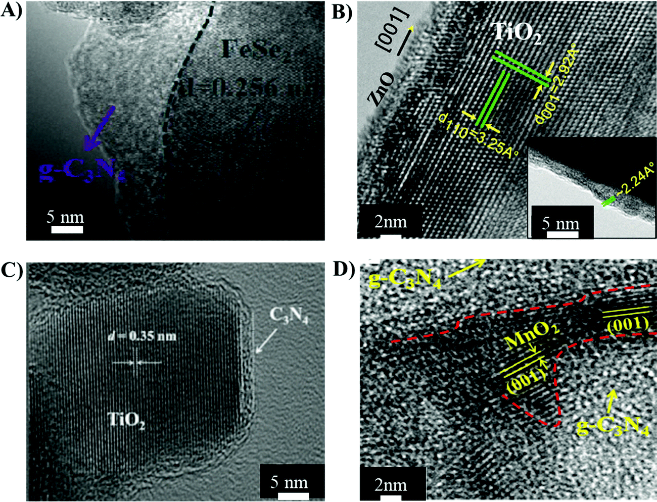 | ||
| Fig. 5 TEM micrographs of (A) the type I FeS2/g-C3N4 heterojunction structure reprinted with permission from Elsevier;88 (B) a type II TiO2/ZnO heterojunction reprinted with permission from Nature;91 (C) a direct Z-scheme g-C3N4-TiO2 heterojunction reprinted with permission from RSC96 and (D) a direct Z-scheme g-C3N4/MnO2 reprinted with permission from ACS publications.98 | ||
3.1.2.1 BiVO4/CeO2. Similarly, a hydrothermal route was employed to synthesise BiVO4/CeO2 type II heterojunction structures, in which BiVO4 and CeO2 had different isoelectric points at pH 4.5 and 7.3, respectively (Table 2, entry 2). BiVO4/CeO2 enabled the photo-catalytic degradation of a mixture of methylene blue (MB) (cationic dye) and methyl orange (MO) (anionic dye) at a kinetic constant of 40 × 10−3 min−1 (Table 2, entry 2).89 Otherwise, the surface charge of single BiVO4 would show electronic repulsion towards anionic dyes such as MO and single CeO2 would show electronic repulsion towards cationic dyes such as MB, leading to no catalytic degradation.89 Therefore, fabrication of the heterojunction not only enhanced the catalytic efficacy by efficient charge separation but also influenced the absorption capabilities by overcoming the electronic repulsion between surface charges and the dye molecules.89
3.1.2.2 MxOx/TiO2 (MxOx = SnO2, NiO). SnO2/TiO2 type-II heterojunctions were prepared by electrophoretic–deposition of P-25 TiO2 on the surface of SnO2 coated glass, followed by annealing at various temperatures from 200–600 °C.90 The kinetic constant of photo-catalytic degradation of rhodamine B using SnO2/TiO2 increased from 2 to 5.5 × 10⁻³ min−1 (Table 2, entry 3) with an increase in the annealing temperature from 100 to 400 °C due to enhanced crystallinity and increased crystallite size from 21 to 39 nm.90 A further increase in temperature to 600 °C led to the conversion of anatase to the rutile phase and aggregation of nanoparticles to form agglomerates of size up to 200 nm, due to which the catalytic efficiency again decreased to 2.5 × 10⁻³ min−1.90
A hydrothermal synthesis route was exploited to develop flower-like type II NiO/TiO2 heterojunction structures (Table 2, entry 4). The fabricated NiO/TiO2 showed a high SSA of 78 m2 g−1 compared to pristine NiO (28 m2 g−1), leading to a greater number of photo-active sites for catalytic reactions along with an enhancement in the absorption capabilities of pollutant molecules on the surface of the catalyst. The photo-catalytic degradation of p-chlorophenol using these NiO/TiO2 hetero-structures showed a kinetic constant of 4.8 × 10⁻³ min−1 (Table 2, entry 4), which was two times higher than that of pristine NiO and TiO2.
3.1.2.3 TiO2/ZnO. A hydrothermal route was also used for the fabrication of type II ZnO–TiO2 nanowires, in which TiO2 nanowires were synthesised by the hydrothermal method, followed by deposition of the ZnO layer via atomic layer deposition (Table 2, entry 5).91 The TEM micrograph of the ZnO–TiO2 nanowires shown in Fig. 5(B) highlights the deposition of ZnO (2.6 nm) on the TiO2 nanowire. The transient photocurrent increased from 0.3 to 0.7 mA cm−2 in the ZnO–TiO2 nanowires compared to pristine TiO2 nanowires, which indicated less recombination of charge carriers and enhanced charge collection ability in the heterojunction structure. The optical band-gap associated with pristine TiO2 was 2.9, while ZnO–TiO2 exhibited a band-gap of 2.6, showing a significant red-shift due to type II band alignments in the core–shell ZnO–TiO2 heterojunction structures and the quantum confinement effect exhibited by the ultrathin layer of ZnO.91 The narrowing of the band-gap extended the light harvesting abilities of the heterojunctions towards visible light.3 The improved electronic and optical properties of the hetero-structures led to an enhancement of the photocatalytic efficiency.92 The photo-catalysis of MB solution using ZnO–TiO2 showed a kinetic constant of 9.5 × 10⁻³ min−1, while pristine TiO2 nanowires degraded MB at a kinetic constant of 5.35 × 10⁻³ min−1.91
TiO2–ZnO heterojunction structures fabricated by the electrospinning and calcination route led to a decrease in the band-gap to 1.17 eV, compared to pristine TiO2 with a 3.2 eV band-gap (Table 2, entry 6). This decrease in band-gap enhanced light absorption and enabled photocatalytic degradation of the dye at lower energy irradiation with a kinetic constant value of 1.3 × 10⁻³ min−1 under direct sunlight.93 However, no band-gap narrowing was observed when Ag doped TiO2/ZnO hetero-structures were fabricated by a sol–gel route (Table 2, entry 7). Ag-TiO2/ZnO exhibited a band-gap in the range of 3.2 to 3.3 eV, similar to the band-gap of pristine TiO2 and ZnO but Ag doping led to the absorption of visible light due to a localised SPR effect. A Xe lamp with a wavelength of 250–765 nm was employed to degrade atrazine using Ag–TiO2/ZnO hetero-structures. Therefore, the conjugation of the SPR effect at the metal/semiconductor junction in the visible region and Schottky-like barrier at the semiconductor/semiconductor interface led to the photo-catalytic degradation of atrazine solution with a kinetic constant of 9.1 × 10⁻³ min−1 (Table 2, entry 7).94
The fabrication of TiO2/ZnO heterojunctions was also explored using magnetron sputtering techniques,95 which led to a deposition of 350 nm thick ZnO layer followed by a 120–200 nm thick TiO2 coating (Table 2, entry 8). The thicker coatings of TiO2 showed the presence of a high fraction of the rutile phase, which provided recombination centres for photo-generated electron and hole pairs, decreasing the separation efficiency and catalytic performance. Therefore, the photocurrent density of TiO2/ZnO (200 nm TiO2 coating) also reduced to 0.01 mA cm−2, while the heterojunction with a 120 nm thick film of TiO2 exhibited a higher photocurrent of 0.35 mA cm−2 and quickly degraded rhodamine B with a kinetic constant of 21 × 10−3 min−1 (Table 2, entry 8).
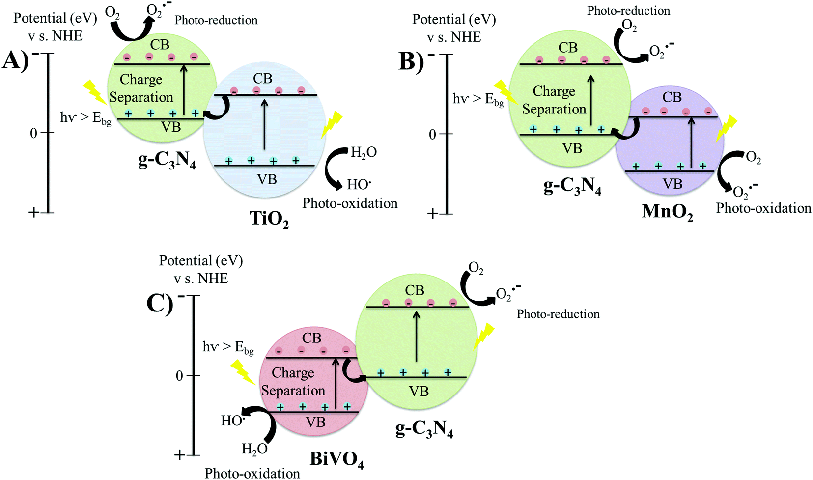
3.1.3.1 g-C3N4-MxOx (MxOx = TiO2, MnO2, BiVO4). Direct-Z scheme heterojunctions were developed by the calcination of a wet mixture of P-25 TiO2 with urea, leading to the fabrication of g-C3N4-TiO2 for the degradation of formaldehyde (Table 2, entry 9).96 The TEM micrographs of g-C3N4-TiO2 revealed a secondary phase of g-C3N4 layers covering the TiO2 granules, shown in Fig. 5(C), which indicated that g-C3N4 did not get incorporated into the lattice but only covered the surface of TiO2. The anatase TiO2 exhibits the CB and VB positions at −0.24 and 2.9 eV vs. NHE, respectively. The CB and VB of g-C3N4 are at −0.85 and 1.85 eV vs. NHE, respectively. Therefore, the electrons migrate from the CB of TiO2 to the VB of g-C3N4 and undergo recombination reactions with the holes of g-C3N4. Meanwhile, upon light irradiation, the electrons are transferred from the VB to the CB of g-C3N4 and the holes located at the VB of TiO2 do not leave their positions, leading to efficient charge separation. The rate constant of photo-catalytic degradation of formaldehyde using Z-Scheme g-C3N4-TiO2 was 70 × 10−3 min−1, about double that of pristine P-25 TiO2 (28 × 10−3 min−1). The degradation mechanism involved the photo-reduction of atmospheric O2 into superoxide ions (˙O2−) at the CB of g-C3N4 by localized electrons. The holes stored in the VB of TiO2 underwent a photo-oxidation reaction by reacting with H2O molecules to produce OH˙ radicals, which were responsible for oxidising the solution of formaldehyde.
If g-C3N4-TiO2 formed a conventional type II heterojunction structure, then electrons from the CB of g-C3N4 would be transferred to the CB of TiO2 and holes would migrate from the VB of TiO2 to the VB of g-C3N4. In this case, the holes localized at the VB of g-C3N4 would not react with water molecules to produce hydroxyl radicals because the VB position of g-C3N4 (1.85 eV) is higher than that of the H2O/OH˙ couple (2.7 eV) vs. NHE, which would result in a lower catalytic efficiency than that of pristine TiO2. Therefore, the heterojunction structure in this study between g-C3N4 and TiO2 was a direct Z-scheme, instead of type II. The charge transfer mechanism of g-C3N4-TiO2 is also represented in Fig. 6(A).96
 | ||
| Fig. 6 Schematic of band structures and charge transfer mechanism in direct Z-scheme heterojunction structures: (A) g-C3N4-TiO2; (B) g-C3N4/MnO2; and (C) TBiVO4/g-C3N4. | ||
The fabrication of direct Z-scheme g-C3N4-TiO2 by a hydrothermal route (Table 2, entry 10),97 which led to the photocatalytic degradation of methyl orange (MO) solution with a kinetic constant of 85 × 10−3 min−1 was also demonstrated. The catalytic efficiency started to decrease with increasing the g-C3N4 content from 70 to 120 mg, as excessive dosage of g-C3N4 led to a decrease in the redox capability of the hetero-structure because of its low conductivity.97 Therefore, it is necessary to optimize the content of semiconducting materials in the hetero-structures for efficient charge separation and catalysis.97
Another direct Z-Scheme heterojunction was fabricated by coupling g-C3N4 and MnO2 by a wet-chemical method (Table 2, entry 11).98 The TEM micrograph presented in Fig. 5(D) shows the integration of g-C3N4 and MnO2. The CB and VB of MnO2 were at 1.22 and 3.5 eV, respectively and the CB and VB of the synthesised g-C3N4 were at −1.6 and 1.73 eV, respectively. Therefore, electrons generated on the CB of MnO2 moved to the VB of g-C3N4 and combined with the holes.98 The electrons on the CB of g-C3N4 reacted with O2 to form superoxide ions (˙O2−), while the holes present on MnO2 reacted with absorbed water molecules to produce hydroxyl radicals (OH˙).98 The charge transfer mechanism of g-C3N4–MnO2 is also presented in Fig. 6(B). Efficient charge separation in the direct Z-scheme g-C3N4/MnO2 heterojunction quickly degraded rhodamine B solution at a kinetic constant of 33 × 10−3 min−1 (Table 2, entry 11).98
The formation of heterojunctions between BiVO4 and g-C3N4 nanosheets also showed a direct Z-Scheme transfer mechanism (Table 2, entry 12),99 whereby the photo-generated electrons generated in the CB of g-C3N4 migrate to the VB of BiVO4 to undergo recombination reactions. Meanwhile, the photo-induced holes remain localised at the VB of BiVO4 to cause photo-reduction reaction and electrons on the CB of g-C3N4 to cause photo-oxidation reactions, as shown in Fig. 6(C). Rhodamine B was photo-catalytically degraded at a kinetic constant of 41 × 10−3 min−1 using the BiVO4/g-C3N4 nanosheet.99
Density functional theory (DFT) calculations are also performed to estimate the physical factors such as relative energy band positions and structures of the heterojunction photocatalysts.100 For instance, the band gaps of CN and CdS in the CN/CdS heterojunction were estimated from the density of states (DOS) calculation to be 2.27 and 2.36 eV, respectively. The CB and VB positions of CdS were found at −0.5 and 1.86 V, which were higher than the CB and VB positions of CN at −1.15 and 1.61V.101 The photo-generated electrons showed migration from CdS to CN, while the holes transferred from CN to CdS. The transfer of charge carriers led to the creation of an internal electric field, which further promotes interfacial charge transfer and inhibits the reverse motion of the charge carriers. Therefore, type II heterojunction structure was predicted for the CN/CdS interface from the energy band position DFT calculations.101 The DOS calculations of another work on CN/SnS2 showed that the CB and VB positions of CN were higher than those of SnS2.102 The internal electric field however supported the migration of week electrons from the CB of SnS2 to the VB of CN, thereby exhibiting a typical direct Z-scheme heterojunction structure.102
The heterojunction materials also showed the advantages of recyclability and reusability for catalytic application.103 The direct Z-scheme heterojunction structure of CeO2/TiO2 led to a total decrease of 1–2% in the catalytic efficiency after three continuous cycles. No deformation in the structure of the heterojunction material was observed in the XRD and XPS spectra, confirming the stability of the material.103 Similarly, another CeO2/CdS heterojunction material showed over 90.5% degradation efficiency even after five cycles, which indicated good recyclability of the heterojunction material.104
3.2 Concluding remarks and strategies for improving heterojunction materials
The engineering of heterojunction structures is one of the most promising approaches towards achieving enhanced catalysis of model pollutant molecules such as methylene blue and rhodamine B, present in wastewater. Conventionally employed heterojunction structures for wastewater treatment are type II and direct Z-Scheme. Type-II heterojunctions support effective spatial charge separation and fast electron transfer mechanisms, leading to a higher catalytic performance than that of pristine semiconducting materials for the degradation of dyes with kinetic constant k = 5–20 × 10−3 min−1. The redox ability of type-II heterojunction materials is somewhat compromised because the photo-reduction reactions occur on semiconducting materials with a lower reduction potential, and photo-oxidation reactions occur on semiconducting material with a lower oxidation potential. The direct Z-scheme heterojunctions offer efficient separation of charge carriers as well as redox ability as the charge transfer mechanism of Z-scheme heterojunctions is opposite to that of type-II heterojunction structures, therefore leading to enhanced catalysis of pollutant molecules with kinetic constant k = 30–70 × 10−3 min−1.Type II and direct Z-scheme heterojunctions have been widely explored over the past few years. After careful reviewing, research gaps and challenges associated with type II and direct Z-scheme heterojunctions have been identified. The charge transfer mechanism of type II heterojunctions is still debatable as it is difficult to achieve the desirable separation of charges in the described mechanism. The redox abilities of the semiconducting photocatalyst are also undermined, which overall attenuates the superior catalytic properties of the heterojunctions. Although, direct Z-scheme heterojunctions seem to overcome the drawbacks of type II heterojunctions still several approaches are required to enhance the photocatalytic performance such as alignment of the Fermi level of the semiconducting materials by doping or employing co-catalysts (Ag, Au, Pt). The incorporation of a suitable co-catalyst can enhance the charge separation as well as reduce the photocatalytic reaction barrier. Rational engineering of the morphology and interface regulation of the heterojunctions lead to enhanced photocatalytic efficiency. For instance, designing 2D/2D heterojunction nanosheets provides a larger area of contact enabling easy flux of electrons across the surface of the heterojunction structures to carry out the redox reactions.83
4 Conclusions, challenges and prospects
Schottky-like and heterojunction structures were discussed to link the charge transfer mechanisms associated with the unique combinatorial arrangement of materials to their catalytic performance. The changes in the physical and photo-electrochemical properties were correlated with the degradation of model pollutants as a route to further improve the general efficiency of relevant photo and electro catalytic processes. Both Schottky-like and heterojunction materials were found to exhibit higher catalytic performance than pristine semiconducting materials towards remediation of organic pollutants due to enhanced charge separation and suppressed recombination of charge carriers.The Schottky-like materials show a non-linear relationship with respect to metal loading, which is interesting since this needs to be carefully optimized to achieve efficient properties and catalytic performance. A major challenge related to the fabrication of Schottky-like materials is the employment of noble metals such as Au, Ag, and Pt to couple with semiconducting materials, as they are present in scarce quantity in nature and also are very costly. The use of conductive non-noble metals or alloys such as stainless steel needs to be explored towards the next generation of more scalable Schottky-like materials.
The semiconductor heterojunction structures also provide an alternative due to their improved electrochemical properties and catalysis compared to those of pristine semiconducting materials without the need for noble metals. The most commonly employed semiconductor heterojunction structures are type-II and direct Z-scheme, which have similar band alignment, but the direction of flow of charge is opposite, and thus can easily be confused with each other. Therefore, the band structures and energy orbitals of the heterojunction materials through theoretical calculations, structural modelling or time-resolved characterization techniques must be explored to acquire the true picture of charge transport mechanisms and intermediate formation during the catalytic reactions. A deeper understanding of the charge separation and transport pathway at the interface will enable the design of new heterojunction structures with better catalytic efficiency. Future work should also be focussed on explaining the plausible charge carrier transfer mechanisms in heterojunction materials comprising more than two semiconducting materials.
Furthermore, the deposition and stabilization of nano-layered Schottky-like or heterojunction structures across conductive and porous substrate materials or membranes106 would mitigate technological issues such as recovery and re-use of catalysts or issues related to mass transfer limitations existing in dense catalytic materials. The Schottky-like or heterojunction membranes represent a highly novel class of separation materials, with improved available surface area and density of catalytically active sites compared to pristine semiconducting materials. Therefore, new strategies and materials for the preparation of Schottky-like and heterojunction structures across conductive membranes are required to enable primary filtration of wastewater with enhanced catalysis at surface and pore structures, high selectivity towards target pollutants, visible light activation, and high photo-stability of the materials.
Conflicts of interest
There are no conflicts to declare.References
- A. Mills and S. Le Hunte, J. Photochem. Photobiol., A, 1997, 108, 1–35 CrossRef CAS.
- H. Tong, S. Ouyang, Y. Bi, N. Umezawa, M. Oshikiri and J. Ye, Adv. Mater., 2012, 24, 229–251 CrossRef CAS PubMed.
- A. Merenda, A. Rana, A. Guirguis, D. M. Zhu, L. Kong and L. F. Dumée, J. Phys. Chem. C, 2019, 123, 2189–2201 CrossRef CAS.
- A. Guirguis, S. R. Polaki, G. Sahoo, S. Ghosh, M. Kamruddin, A. Merenda, X. Chen, J. W. Maina, G. Szekely and L. Dumee, Carbon, 2020, 168, 32–41 CrossRef CAS.
- R. T. Tung, Mater. Sci. Eng., R, 2001, 35, 1–138 CrossRef.
- X. Ding, Y. Zhao, H. Xiao and L. Qiao, Appl. Phys. Lett., 2021, 118, 091601 CrossRef CAS.
- X. Feng, C. Huang, V. Lui, R. Khangura and Z. Lu, Appl. Phys. Lett., 2005, 86, 143511 CrossRef.
- Y.-s. Fu, J. Li and J. Li, Nanomaterials, 2019, 9, 359 CrossRef CAS PubMed.
- R. Ghita, C. Logofatu, C. Negrila, A. Manea, M. Cernea and M. Lazarescu, J. Optoelectron. Adv. Mater., 2005, 7, 3033–3037 CAS.
- H. Wang, L. Zhang, Z. Chen, J. Hu, S. Li, Z. Wang, J. Liu and X. Wang, Chem. Soc. Rev., 2014, 43, 5234–5244 RSC.
- B. Sharma and R. Purohit, Semiconductor heterojunctions, Elsevier, 2015 Search PubMed.
- Q. Su, Y. Li, R. Hu, F. Song, S. Liu, C. Guo, S. Zhu, W. Liu and J. Pan, Adv. Sustainable Syst., 2020, 4, 2000130 CrossRef CAS.
- H. Li, H. Hu, C. Bao, F. Guo, X. Zhang, X. Liu, J. Hua, J. Tan, A. Wang, H. Zhou, B. Yang, Y. Qu and X. Liu, Sci. Rep., 2016, 6, 29327 CrossRef CAS PubMed.
- X. Kong, L. Zhang, B. Liu, H. Gao, Y. Zhang, H. Yan and X. Song, RSC Adv., 2019, 9, 863–877 RSC.
- M. Farhat, S. Kais and F. H. Alharbi, Sci. Rep., 2017, 7, 14253 CrossRef CAS PubMed.
- A. J. Wirth-Lima, P. P. Alves-Sousa and W. Bezerra-Fraga, SN Appl. Sci., 2020, 2, 246 CrossRef CAS.
- Y.-S. Fu, J. Li and J. Li, Nanomaterials, 2019, 9, 359 CrossRef CAS PubMed.
- M. R. Khan, T. W. Chuan, A. Yousuf, M. N. K. Chowdhury and C. K. Cheng, Catal. Sci. Technol., 2015, 5, 2522–2531 RSC.
- J. Low, J. Yu, M. Jaroniec, S. Wageh and A. A. Al-Ghamdi, Adv. Mater., 2017, 29, 1601694 CrossRef PubMed.
- F. Teng, K. Hu, W. Ouyang and X. Fang, Adv. Mater., 2018, 30, 1706262 CrossRef PubMed.
- G. L. Chiarello, M. H. Aguirre and E. Selli, J. Catal., 2010, 273, 182–190 CrossRef CAS.
- C. Young, T. M. Lim, K. Chiang, J. Scott and R. Amal, Appl. Catal., B, 2008, 78, 1–10 CrossRef CAS.
- K. Gurunathan, Int. J. Hydrogen Energy, 2004, 29, 933–940 CrossRef CAS.
- Z. Yi, A. Merenda, L. Kong, A. Radenovic, M. Majumder and L. F. Dumée, Sci. Rep., 2018, 8, 8154 CrossRef PubMed.
- J.-D. Xiao, L. Han, J. Luo, S.-H. Yu and H.-L. Jiang, Angew. Chem., Int. Ed., 2018, 57, 1103–1107 CrossRef CAS PubMed.
- S. Zhang, H. Lu, G. Rui, C. Lv, J. He, Y. Cui and B. Gu, Appl. Phys. B: Lasers Opt., 2020, 126, 135 CrossRef CAS.
- J. W. Maina, A. Merenda, M. Weber, J. M. Pringle, M. Bechelany, L. Hyde and L. F. Dumée, Crit. Rev. Solid State Mater. Sci., 2020, 1–22, DOI:10.1080/10408436.2020.1819200.
- J. A. Dionne and H. A. Atwater, MRS Bull., 2012, 37, 717–724 CrossRef CAS.
- S. C. Warren and E. Thimsen, Energy Environ. Sci., 2012, 5, 5133–5146 RSC.
- S. Zeng, K.-T. Yong, I. Roy, X.-Q. Dinh, X. Yu and F. Luan, Plasmonics, 2011, 6, 491 CrossRef CAS.
- S. Seong, I.-S. Park, Y. C. Jung, T. Lee, S. Y. Kim, J. S. Park, J.-H. Ko and J. Ahn, Mater. Des., 2019, 177, 107831 CrossRef CAS.
- A. P. Manuel and K. Shankar, Nanomaterials, 2021, 11, 1249 CrossRef CAS PubMed.
- A. Zada, P. Muhammad, W. Ahmad, Z. Hussain, S. Ali, M. Khan, Q. Khan and M. Maqbool, Adv. Funct. Mater., 2020, 30, 1906744 CrossRef CAS.
- X. Zhu, J. Wang, D. Yang, J. Liu, L. He, M. Tang, W. Feng and X. Wu, RSC Adv., 2021, 11, 27257–27266 RSC.
- A. Merenda, M. Weber, M. Bechelany, F.-M. Allioux, L. Hyde, L. Kong and L. F. Dumée, Appl. Surf. Sci., 2019, 483, 219–230 CrossRef CAS.
- J. Z. Y. Tan, Y. Fernández, D. Liu, M. Maroto-Valer, J. Bian and X. Zhang, Chem. Phys. Lett., 2012, 531, 149–154 CrossRef CAS.
- L. J. Brillson, Surf. Sci. Rep., 1982, 2, 123–326 CrossRef CAS.
- J. Yu, L. Qi and M. Jaroniec, J. Phys. Chem. C, 2010, 114, 13118–13125 CrossRef CAS.
- C.-H. Lin, J.-H. Chao, C.-H. Liu, J.-C. Chang and F.-C. Wang, Langmuir, 2008, 24, 9907–9915 CrossRef CAS PubMed.
- H. Shi, X. Wang, M. Zheng, X. Wu, Y. Chen, Z. Yang, G. Zhang and H. Duan, Adv. Mater. Interfaces, 2016, 3, 1600588 CrossRef.
- P. K. Kalambate, Dhanjai, Z. Huang, Y. Li, Y. Shen, M. Xie, Y. Huang and A. K. Srivastava, TrAC, Trends Anal. Chem., 2019, 115, 147–161 CrossRef CAS.
- R. Nawaz, C. F. Kait, H. Y. Chia, M. H. Isa and L. W. Huei, Environ. Technol. Innovation, 2020, 19, 101007 CrossRef.
- P. Kumari, N. Bahadur, L. A. O'Dell, L. Kong, A. Sadek, A. Merenda and L. F. Dumée, Sep. Purif. Technol., 2021, 258, 118011 CrossRef CAS.
- J. Li and H. C. Zeng, Angew. Chem., Int. Ed., 2005, 44, 4342–4345 CrossRef CAS PubMed.
- J. Ghilane, F.-R. F. Fan, A. J. Bard and N. Dunwoody, Nano Lett., 2007, 7, 1406–1412 CrossRef CAS PubMed.
- Y. F. Zhu, D. H. Fan and W. Z. Shen, J. Phys. Chem. C, 2008, 112, 10402–10406 CrossRef CAS.
- H. Liu, X. Dong, X. Wang, C. Sun, J. Li and Z. Zhu, Chem. Eng. J., 2013, 230, 279–285 CrossRef CAS.
- S. Son, J. M. Lee, S.-J. Kim, H. Kim, X. Jin, K. K. Wang, M. Kim, J. W. Hwang, W. Choi, Y.-R. Kim, H. Kim and S.-J. Hwang, Appl. Catal., B, 2019, 257, 117875 CrossRef CAS.
- Z. Sun, T. Liao, Y. Dou, S. M. Hwang, M.-S. Park, L. Jiang, J. H. Kim and S. X. Dou, Nat. Commun., 2014, 5, 3813 CrossRef CAS PubMed.
- J. A. Singh, N. F. W. Thissen, W.-H. Kim, H. Johnson, W. M. M. Kessels, A. A. Bol, S. F. Bent and A. J. M. Mackus, Chem. Mater., 2018, 30, 663–670 CrossRef CAS PubMed.
- B. C. Mallick, C.-T. Hsieh, K.-M. Yin, Y. A. Gandomi and K.-T. Huang, ECS J. Solid State Sci. Technol., 2019, 8, N55–N78 CrossRef CAS.
- P. Zhou, J. Yu and M. Jaroniec, Adv. Mater., 2014, 26, 4920–4935 CrossRef CAS PubMed.
- H. Tada, T. Mitsui, T. Kiyonaga, T. Akita and K. Tanaka, Nat. Mater., 2006, 5, 782–786 CrossRef CAS PubMed.
- C. Ren, B. Yang, M. Wu, J. Xu, Z. Fu, Y. lv, T. Guo, Y. Zhao and C. Zhu, J. Hazard. Mater., 2010, 182, 123–129 CrossRef CAS PubMed.
- C. Dahmen, A. N. Sprafke, H. Dieker, M. Wuttig and G. V. Plessen, Appl. Phys. Lett., 2006, 88, 011923 CrossRef.
- Z. Jiang, W. Wei, D. Mao, C. Chen, Y. Shi, X. Lv and J. Xie, Nanoscale, 2015, 7, 784–797 RSC.
- O. Bechambi, M. Chalbi, W. Najjar and S. Sayadi, Appl. Surf. Sci., 2015, 347, 414–420 CrossRef CAS.
- X. Zhu, X. Liang, P. Wang, Y. Dai and B. Huang, Appl. Surf. Sci., 2018, 456, 493–500 CrossRef CAS.
- S. T. Kochuveedu, D.-P. Kim and D. H. Kim, J. Phys. Chem. C, 2012, 116, 2500–2506 CrossRef CAS.
- S. Cao, F. Tao, Y. Tang, Y. Li and J. Yu, Chem. Soc. Rev., 2016, 45, 4747–4765 RSC.
- J. Adekoya, O. Olurotimi, T. Siyanbola, E. Dare and N. Revaprasadu, Band structure, Morphology, Functionality, and size dependent properties of metal nanoparticles, Nobel and precious metals properties, nanoscale effects and applications, IntechOpen, 2018, pp. 15–41 Search PubMed.
- T.-T. Yang, W.-T. Chen, Y.-J. Hsu, K.-H. Wei, T.-Y. Lin and T.-W. Lin, J. Phys. Chem. C, 2010, 114, 11414–11420 CrossRef CAS.
- H. Wang, W. Zhao, C.-H. Xu, H.-Y. Chen and J.-J. Xu, Chem. Sci., 2019, 10, 9308–9314 RSC.
- S. T. Kochuveedu, Y. H. Jang and D. H. Kim, Chem. Soc. Rev., 2013, 42, 8467–8493 RSC.
- V. L. Chandraboss, Mater. Today: Proc., 2021, 36, 907–913 CAS.
- R. Rahimi, M. Heidari-Golafzani and M. Rabbani, Superlattices Microstruct., 2015, 85, 497–503 CrossRef CAS.
- F. Dong, Z. Zhao, Y. Sun, Y. Zhang, S. Yan and Z. Wu, Environ. Sci. Technol., 2015, 49, 12432–12440 CrossRef CAS PubMed.
- Y. Gao, Y. Huang, Y. Li, Q. Zhang, J.-J. Cao, W. Ho and S. C. Lee, ACS Sustainable Chem. Eng., 2016, 4, 6912–6920 CrossRef CAS.
- Y. Zhang, C. Yuan, Q. Wang, M. R. Hoffmann, X. Zhang, J. Nie, C. Hu, S. Chen, J. Qiao, Q. Wang and Y. Cong, Electrochim. Acta, 2019, 328, 135124 CrossRef CAS.
- C. Yao, J. Lin, L. Li, Y. Qu, K. Jiang, Z. Hu, N. Xu, J. Sun and J. Wu, J. Phys. Chem. C, 2020, 124, 10941–10950 CrossRef CAS.
- X. He, T. Kai and P. Ding, Environ. Chem. Lett., 2021, 19, 4563–4601 CrossRef CAS PubMed.
- L. Wei, C. Yu, Q. Zhang, H. Liu and Y. Wang, J. Mater. Chem. A, 2018, 6, 22411–22436 RSC.
- S. Perlman and D. Feucht, Solid-State Electron., 1964, 7, 911–923 CrossRef.
- T. Trindade, P. O'Brien and N. L. Pickett, Chem. Mater., 2001, 13, 3843–3858 CrossRef CAS.
- B. Yacobi, Semiconductor Materials: An Introduction to Basic Principles, 2003, pp. 135–170 Search PubMed.
- F. Mei, K. Dai, J. Zhang, W. Li and C. Liang, Appl. Surf. Sci., 2019, 488, 151–160 CrossRef CAS.
- J. Wang, Q. Zhang, F. Deng, X. Luo and D. D. Dionysiou, Chem. Eng. J., 2020, 379, 122264 CrossRef CAS.
- X. Jia, Q. Han, M. Zheng and H. Bi, Appl. Surf. Sci., 2019, 489, 409–419 CrossRef CAS.
- Q. Xu, L. Zhang, J. Yu, S. Wageh, A. A. Al-Ghamdi and M. Jaroniec, Mater. Today, 2018, 21, 1042–1063 CrossRef CAS.
- Q. Xu, L. Zhang, B. Cheng, J. Fan and J. Yu, Chem, 2020, 6, 1543–1559 CAS.
- X. Li, J. Liu, J. Huang, C. He, Z. Feng, Z. Chen, L. Wan and F. Deng, Acta Phys.-Chim. Sin., 2020, 37, 2010030 Search PubMed.
- T. Di, Q. Xu, W. Ho, H. Tang, Q. Xiang and J. Yu, ChemCatChem, 2019, 11, 1394–1411 CrossRef CAS.
- F. He, A. Meng, B. Cheng, W. Ho and J. Yu, Chin. J. Catal., 2020, 41, 9–20 CrossRef CAS.
- J. Mu, F. Teng, H. Miao, Y. Wang and X. Hu, Appl. Surf. Sci., 2020, 501, 143974 CrossRef CAS.
- R. Wang, J. Shen, W. Zhang, Q. Liu, M. Zhang, Zulfiqar and H. Tang, Ceram. Int., 2020, 46, 23–30 CrossRef CAS.
- J. Low, C. Jiang, B. Cheng, S. Wageh, A. A. Al-Ghamdi and J. Yu, Small Methods, 2017, 1, 1700080 CrossRef.
- J. Su, G.-D. Li, X.-H. Li and J.-S. Chen, Adv. Sci., 2019, 6, 1801702 CrossRef PubMed.
- J. Jia, W. Sun, Q. Zhang, X. Zhang, X. Hu, E. Liu and J. Fan, Appl. Catal., B, 2020, 261, 118249 CrossRef CAS.
- N. Wetchakun, S. Chaiwichain, B. Inceesungvorn, K. Pingmuang, S. Phanichphant, A. I. Minett and J. Chen, ACS Appl. Mater. Interfaces, 2012, 4, 3718–3723 CrossRef CAS PubMed.
- M. Zhou, J. Yu, S. Liu, P. Zhai and L. Jiang, J. Hazard. Mater., 2008, 154, 1141–1148 CrossRef CAS PubMed.
- A. Ghobadi, T. G. Ulusoy, R. Garifullin, M. O. Guler and A. K. Okyay, Sci. Rep., 2016, 6, 30587 CrossRef CAS PubMed.
- S. Li, C. Wang, M. Cai, F. Yang, Y. Liu, J. Chen, P. Zhang, X. Li and X. Chen, Chem. Eng. J., 2022, 428, 131158 CrossRef CAS.
- H. M. Mousa, J. F. Alenezi, I. M. A. Mohamed, A. S. Yasin, A.-F. M. Hashem and A. Abdal-hay, J. Alloys Compd., 2021, 886, 161169 CrossRef CAS.
- C. Belver, M. Hinojosa, J. Bedia, M. Tobajas, M. A. Alvarez, V. Rodríguez-González and J. J. Rodriguez, Materials, 2017, 10, 960 CrossRef PubMed.
- H. Ma, B. Hao, W. Song, J. Guo, M. Li and L. Zhang, Materials, 2021, 14, 3299 CrossRef CAS PubMed.
- J. Yu, S. Wang, J. Low and W. Xiao, Phys. Chem. Chem. Phys., 2013, 15, 16883–16890 RSC.
- W. Gu, F. Lu, C. Wang, S. Kuga, L. Wu, Y. Huang and M. Wu, ACS Appl. Mater. Interfaces, 2017, 9, 28674–28684 CrossRef CAS PubMed.
- P. Xia, B. Zhu, B. Cheng, J. Yu and J. Xu, ACS Sustainable Chem. Eng., 2018, 6, 965–973 CrossRef CAS.
- Z. Sun, Z. Yu, Y. Liu, C. Shi, M. Zhu and A. Wang, J. Colloid Interface Sci., 2019, 533, 251–258 CrossRef CAS PubMed.
- J. Xue and J. Bao, Surf. Interfaces, 2021, 25, 101265 CrossRef CAS.
- J. Liu, J. Phys. Chem. C, 2015, 119, 28417–28423 CrossRef CAS.
- J. Liu and E. Hua, J. Phys. Chem. C, 2017, 121, 25827–25835 CrossRef CAS.
- H. Yan, R. Wang, R. Liu, T. Xu, J. Sun, L. Liu and J. Wang, Appl. Catal., B, 2021, 291, 120096 CrossRef CAS.
- R. Zou, L. Li, L. Yang, J. Lan, H. Liu, B. Dou, J. Shang and S. Lin, Cellulose, 2021, 28, 11081–11096 CrossRef.
- J. Yu, W. Wang and B. Cheng, Chem. – Asian J., 2010, 5, 2499–2506 CrossRef CAS PubMed.
- P. Kumari, N. Bahadur, M. Cretin, L. Kong, L. A. O'Dell, A. Merenda and L. F. Dumée, React. Chem. Eng., 2021, 6, 1508–1526 RSC.
| This journal is © The Royal Society of Chemistry 2022 |